US4698662A - Multichip thin film module - Google Patents
Multichip thin film module Download PDFInfo
- Publication number
- US4698662A US4698662A US06/698,472 US69847285A US4698662A US 4698662 A US4698662 A US 4698662A US 69847285 A US69847285 A US 69847285A US 4698662 A US4698662 A US 4698662A
- Authority
- US
- United States
- Prior art keywords
- package
- heat sink
- thermal
- heat
- substrate
- Prior art date
- Legal status (The legal status is an assumption and is not a legal conclusion. Google has not performed a legal analysis and makes no representation as to the accuracy of the status listed.)
- Expired - Lifetime
Links
Images

Classifications
-
- H—ELECTRICITY
- H01—ELECTRIC ELEMENTS
- H01L—SEMICONDUCTOR DEVICES NOT COVERED BY CLASS H10
- H01L23/00—Details of semiconductor or other solid state devices
- H01L23/12—Mountings, e.g. non-detachable insulating substrates
- H01L23/14—Mountings, e.g. non-detachable insulating substrates characterised by the material or its electrical properties
- H01L23/147—Semiconductor insulating substrates
-
- H—ELECTRICITY
- H01—ELECTRIC ELEMENTS
- H01L—SEMICONDUCTOR DEVICES NOT COVERED BY CLASS H10
- H01L23/00—Details of semiconductor or other solid state devices
- H01L23/34—Arrangements for cooling, heating, ventilating or temperature compensation ; Temperature sensing arrangements
- H01L23/36—Selection of materials, or shaping, to facilitate cooling or heating, e.g. heatsinks
- H01L23/373—Cooling facilitated by selection of materials for the device or materials for thermal expansion adaptation, e.g. carbon
- H01L23/3738—Semiconductor materials
-
- H—ELECTRICITY
- H01—ELECTRIC ELEMENTS
- H01L—SEMICONDUCTOR DEVICES NOT COVERED BY CLASS H10
- H01L23/00—Details of semiconductor or other solid state devices
- H01L23/52—Arrangements for conducting electric current within the device in operation from one component to another, i.e. interconnections, e.g. wires, lead frames
- H01L23/538—Arrangements for conducting electric current within the device in operation from one component to another, i.e. interconnections, e.g. wires, lead frames the interconnection structure between a plurality of semiconductor chips being formed on, or in, insulating substrates
-
- H—ELECTRICITY
- H01—ELECTRIC ELEMENTS
- H01L—SEMICONDUCTOR DEVICES NOT COVERED BY CLASS H10
- H01L2224/00—Indexing scheme for arrangements for connecting or disconnecting semiconductor or solid-state bodies and methods related thereto as covered by H01L24/00
- H01L2224/01—Means for bonding being attached to, or being formed on, the surface to be connected, e.g. chip-to-package, die-attach, "first-level" interconnects; Manufacturing methods related thereto
- H01L2224/10—Bump connectors; Manufacturing methods related thereto
- H01L2224/15—Structure, shape, material or disposition of the bump connectors after the connecting process
- H01L2224/16—Structure, shape, material or disposition of the bump connectors after the connecting process of an individual bump connector
- H01L2224/161—Disposition
- H01L2224/16151—Disposition the bump connector connecting between a semiconductor or solid-state body and an item not being a semiconductor or solid-state body, e.g. chip-to-substrate, chip-to-passive
- H01L2224/16221—Disposition the bump connector connecting between a semiconductor or solid-state body and an item not being a semiconductor or solid-state body, e.g. chip-to-substrate, chip-to-passive the body and the item being stacked
- H01L2224/16225—Disposition the bump connector connecting between a semiconductor or solid-state body and an item not being a semiconductor or solid-state body, e.g. chip-to-substrate, chip-to-passive the body and the item being stacked the item being non-metallic, e.g. insulating substrate with or without metallisation
-
- H—ELECTRICITY
- H01—ELECTRIC ELEMENTS
- H01L—SEMICONDUCTOR DEVICES NOT COVERED BY CLASS H10
- H01L2924/00—Indexing scheme for arrangements or methods for connecting or disconnecting semiconductor or solid-state bodies as covered by H01L24/00
- H01L2924/01—Chemical elements
- H01L2924/01014—Silicon [Si]
-
- H—ELECTRICITY
- H01—ELECTRIC ELEMENTS
- H01L—SEMICONDUCTOR DEVICES NOT COVERED BY CLASS H10
- H01L2924/00—Indexing scheme for arrangements or methods for connecting or disconnecting semiconductor or solid-state bodies as covered by H01L24/00
- H01L2924/10—Details of semiconductor or other solid state devices to be connected
- H01L2924/102—Material of the semiconductor or solid state bodies
- H01L2924/1025—Semiconducting materials
- H01L2924/10251—Elemental semiconductors, i.e. Group IV
- H01L2924/10253—Silicon [Si]
-
- H—ELECTRICITY
- H01—ELECTRIC ELEMENTS
- H01L—SEMICONDUCTOR DEVICES NOT COVERED BY CLASS H10
- H01L2924/00—Indexing scheme for arrangements or methods for connecting or disconnecting semiconductor or solid-state bodies as covered by H01L24/00
- H01L2924/15—Details of package parts other than the semiconductor or other solid state devices to be connected
- H01L2924/151—Die mounting substrate
- H01L2924/153—Connection portion
- H01L2924/1531—Connection portion the connection portion being formed only on the surface of the substrate opposite to the die mounting surface
- H01L2924/15312—Connection portion the connection portion being formed only on the surface of the substrate opposite to the die mounting surface being a pin array, e.g. PGA
Definitions
- the invention relates generally to thermal-dissipation techniques for integrated-circuit technology and more specifically relates to multichip thin-film interconnect modules having high thermal dissipation requirements.
- the present technology for packaging integrated circuits typically involves placement of a plurality of integrated circuits on a relatively large multiplayer board.
- the boards are typically formed of glass epoxy or thick polyimide substrates.
- the integrated circuit chips are typically widely spaced on the board such that the power density required to be dissipated is on the order of less than 0.2 watts per centimeter square.
- the power density required to be dissipated is on the order of less than 0.2 watts per centimeter square.
- the power dissipation per chip also drastically increases as the speed of the integrated circuit chips increases.
- the anticipated power density can be as high as six watts per centimeter square in future generations of high speed computers.
- one of the objectives of packaging techniques for future generation integrated-circuit devices is to be able to dissipate significantly more heat than is currently being dissipated using traditional packaging technology.
- Another problem associated with increased heat dissipation and generation is that any thermal mismatch between the integrated-circuit chip package and its underlying multilayer circuit board will be undesirably intensified.
- the invention can be briefly described as a package for thermal dissipation of heat from multiple integrated circuit chips.
- the subject invention includes a silicon substrate containing thin-film multilayer interconnect planes. Multiple integrated circuit chips can be attached to a first surface of a substrate.
- the invention further includes a means for dissipating heat from a second surface of the silicon substrate.
- An object of the invention is to provide a means to dissipate up to six watts per square centimeter of heat generated by integrated circuit chips.
- Another object of the invention is to provide a heat-dissipation package for multiple integrated-circuit chips using a single substrate and heat sink.
- Another object of the invention is to provide a heat-dissipation package for multiple integrated-circuit chips in which a single heat sink can be adapted to liquid-cooling techniques.
- Another object of the invention is to provide a silicon substrate for silicon integrated-circuit chips in which the substrate includes a plurality of cavities, each cavity being designed to accept an individual integrated-circuit chip.
- Another object of the invention is to provide a package for enhanced thermal dissipation of heat from integrated-circuit chips having high reliability thus reducing the operating temperature of the chip and reducing the possibility of thermally induced detachment of the chip for its substrate.
- Another object of the invention is to provide a highly efficient thermal dissipation package for multiple integrated-circuit chips which is capable of being produced commercially at a low cost.
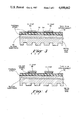
- FIG. 1 is a schematic cross-sectional view of a multichip thin-film module
- FIG. 2 illustrates one embodiment of the subject invention in which integrated circuit chips are epoxy bonded onto a silicon substrate containing thin-film interconnect planes;
- FIG. 4 is a side view of yet another embodiment of the subject invention in which flip chip bonding is employed to attach multiple integrated-circuit chips to a silicon substrate.
- a plurality of integrated circuits 12,14 are attached to a silicon substrate 16.
- the silicon substrate 16 includes multiple layers of thin-film interconnects 18.
- the silicon substrate and its multilayered thin-film interconnects are more fully described in co-pending application Ser. No. 697,092 filed Jan. 31, 1985 entitled A DEVICE AND METHOD FOR FORMING THIN-FILM ELECTRICAL CONNECTIONS FOR INTEGRATED CIRCUITS.
- a heat sink 20 is provided which is contiguous with one surface 22 of the silicon substrate 16.
- a ceramic ring 24 may be provided which contains multiple pins 26 for insertion into a multilayer printed-circuit board (not shown).
- bipolar integrated circuit chips of future-generation devices may be between 6 millimeter square to 1 centimeter square and have up to 10,000 logic gates per chip. It is envisioned that such devices would have a heat-generation characteristic of approximately 10 to 15 watts per chip.
- the subject invention comprehends that such future bipolar integrated-circuit chips 28 can be attached to a silicon substrate 30 having thin-film interconnect planes 32.
- a thermal epoxy 34 such as Aremco 568, a trademark of Aremco Products, N.Y.
- Aremco 568 epoxy is used in the preferred embodiment, other materials may be used such as Abletherm, a trademark of Ablestick Laboratories, Cal., provided that the material used has sufficient adherence characteristics to maintain the semiconductor chip on the substrate and provided that the material used has sufficient resilience to absorb any thermally induced stress. In addition, the material used must have a thermal conductivity on the order of 0.02 watts per centimeter-degree centigrade.
- a second surface of the silicon substrate 30 is provided with a second layer of thermal epoxy 42.
- a metal heat sink 40 is attached to the second surface of the silicon substrate using thermal epoxy layer 42.
- any material may be used as the heat sink provided that it has high thermal conductivity, is easy to machine or to manufacture, and is relatively inexpensive.
- copper, molybdenum, and aluminum may be used as the heat sink material.
- the preferred embodiment of the subject invention envisions that the heat sink 40 include fins or other surface-maximizing means to increase the capacity of the heat sink to dissipate heat into the environment.
- a single cooling source may be easily used to provide additional heat dissipation capabilities to the heat sink.
- a fan (not shown) may be used to produce forced-air cooling across heat sink 40.
- liquid cooling may be provided in a single unit to heat sink 40 to provide additional heat dissipation to the multiple integrated-circuit chips 28.
- FIG. 3 another embodiment of the subject invention envisions that integrated circuit chips 48,50 may be located in a series of cavities 52,54 provided in the upper surface of the silicon substrate.
- the silicon substrate 56 includes multiple layers of thin-film interconnects 58 sandwiched between a dielectric polymer.
- the embodiment illustrated in FIG. 3 has several advantages over the embodiment illustrated in FIG. 2. For example, the placement substrate rather than on top of the thin-film interconnect planes 32 increases the heat transfer from the integrated circuit chip to the underlying silicon substrate.
- Another advantage of placing the integrated circuit chip in cavities is that it virtually eliminates the possibility of any problems arising from a thermal expansion mismatch between the integrated circuit chip and its support. This increases the reliability of the structure since the possibility of detachment of any electrical connections between the chip and its support are reduced.
- FIG. 4 Another embodiment of the subject invention is illustrated in FIG. 4.
- flip chips is an integrated circuit chip in which numerous input-output pads are provided either around the perimeter or over the entire surface of a chip. The surface of the chip on which the input-output pads are located is then positioned adjacent to the surface of the support material containing the electrical terminals (commonly called solder bumps 60) to which the integrated circuit is to be attached.
- the subject invention comprehends that either wire bonding or automated tape bonding is used in the embodiments used in FIGS. 2 and 3 is preferred over solder bump bonding as used in FIG. 4. However, in some embodiments it may be desirable to use solder bump bonding since the number of input-output pads can be maximized using this technique.
Abstract
Description
Claims (12)
Priority Applications (1)
| Application Number | Priority Date | Filing Date | Title |
|---|---|---|---|
| US06/698,472 US4698662A (en) | 1985-02-05 | 1985-02-05 | Multichip thin film module |
Applications Claiming Priority (1)
| Application Number | Priority Date | Filing Date | Title |
|---|---|---|---|
| US06/698,472 US4698662A (en) | 1985-02-05 | 1985-02-05 | Multichip thin film module |
Publications (1)
| Publication Number | Publication Date |
|---|---|
| US4698662A true US4698662A (en) | 1987-10-06 |
Family
ID=24805398
Family Applications (1)
| Application Number | Title | Priority Date | Filing Date |
|---|---|---|---|
| US06/698,472 Expired - Lifetime US4698662A (en) | 1985-02-05 | 1985-02-05 | Multichip thin film module |
Country Status (1)
| Country | Link |
|---|---|
| US (1) | US4698662A (en) |
Cited By (34)
| Publication number | Priority date | Publication date | Assignee | Title |
|---|---|---|---|---|
| US4743568A (en) * | 1987-07-24 | 1988-05-10 | Motorola Inc. | Multilevel interconnect transfer process |
| US4835598A (en) * | 1985-06-13 | 1989-05-30 | Matsushita Electric Works, Ltd. | Wiring board |
| US4874721A (en) * | 1985-11-11 | 1989-10-17 | Nec Corporation | Method of manufacturing a multichip package with increased adhesive strength |
| US4907067A (en) * | 1988-05-11 | 1990-03-06 | Texas Instruments Incorporated | Thermally efficient power device package |
| US5040052A (en) * | 1987-12-28 | 1991-08-13 | Texas Instruments Incorporated | Compact silicon module for high density integrated circuits |
| US5051865A (en) * | 1985-06-17 | 1991-09-24 | Fujitsu Limited | Multi-layer semiconductor device |
| US5055909A (en) * | 1990-05-14 | 1991-10-08 | Vlsi Technology, Inc | System for achieving desired bondlength of adhesive between a semiconductor chip package and a heatsink |
| US5055907A (en) * | 1989-01-25 | 1991-10-08 | Mosaic, Inc. | Extended integration semiconductor structure with wiring layers |
| DE4116321A1 (en) * | 1991-05-16 | 1991-11-28 | Ermic Gmbh | Assembly of sensor-chip on printed circuit board - obtd. by gluing chip to carrier material, attaching to PCB inside ring shaped barrier and filling by injection moulding |
| EP0460785A1 (en) * | 1990-06-05 | 1991-12-11 | Mitsubishi Denki Kabushiki Kaisha | Semiconductor device having a heat sink |
| US5151776A (en) * | 1989-03-28 | 1992-09-29 | General Electric Company | Die attachment method for use in high density interconnected assemblies |
| US5192716A (en) * | 1989-01-25 | 1993-03-09 | Polylithics, Inc. | Method of making a extended integration semiconductor structure |
| US5206713A (en) * | 1990-06-29 | 1993-04-27 | Digital Equipment Corporation | Mounting silicon chips |
| US5220487A (en) * | 1992-01-27 | 1993-06-15 | International Business Machines Corporation | Electronic package with enhanced heat sinking |
| US5262719A (en) * | 1991-09-19 | 1993-11-16 | International Business Machines Corporation | Test structure for multi-layer, thin-film modules |
| US5317194A (en) * | 1989-10-17 | 1994-05-31 | Kabushiki Kaisha Toshiba | Resin-sealed semiconductor device having intermediate silicon thermal dissipation means and embedded heat sink |
| US5413964A (en) * | 1991-06-24 | 1995-05-09 | Digital Equipment Corporation | Photo-definable template for semiconductor chip alignment |
| US5461201A (en) * | 1993-01-22 | 1995-10-24 | Siemens Aktiengesellschaft | Insulating part with integral cooling element |
| US5500540A (en) * | 1994-04-15 | 1996-03-19 | Photonics Research Incorporated | Wafer scale optoelectronic package |
| EP0777275A2 (en) * | 1995-11-30 | 1997-06-04 | Mitsubishi Denki Kabushiki Kaisha | Semiconductor module with heat sink |
| US5815427A (en) * | 1997-04-02 | 1998-09-29 | Micron Technology, Inc. | Modular memory circuit and method for forming same |
| US5953210A (en) * | 1997-07-08 | 1999-09-14 | Hughes Electronics Corporation | Reworkable circuit board assembly including a reworkable flip chip |
| US5972736A (en) * | 1994-12-21 | 1999-10-26 | Sun Microsystems, Inc. | Integrated circuit package and method |
| US6191476B1 (en) * | 1992-10-21 | 2001-02-20 | Seiko Instruments Inc. | Semiconductor device |
| US6243508B1 (en) | 1999-06-01 | 2001-06-05 | Picolight Incorporated | Electro-opto-mechanical assembly for coupling a light source or receiver to an optical waveguide |
| US20030174455A1 (en) * | 2002-03-15 | 2003-09-18 | Vijay Kataria | Thermal dissipation assembly for electronic components |
| US6800948B1 (en) * | 2002-07-19 | 2004-10-05 | Asat Ltd. | Ball grid array package |
| US20060223229A1 (en) * | 2002-07-19 | 2006-10-05 | Asat Ltd. | Ball grid array package and process for manufacturing same |
| US20080011289A1 (en) * | 2006-07-14 | 2008-01-17 | National Science And Technology Development Agency | Photovoltaic thermal (PVT) collector |
| US7371610B1 (en) | 2002-07-19 | 2008-05-13 | Asat Ltd. | Process for fabricating an integrated circuit package with reduced mold warping |
| US7372151B1 (en) | 2003-09-12 | 2008-05-13 | Asat Ltd. | Ball grid array package and process for manufacturing same |
| US8610262B1 (en) | 2005-02-18 | 2013-12-17 | Utac Hong Kong Limited | Ball grid array package with improved thermal characteristics |
| US20140367860A1 (en) * | 2013-06-18 | 2014-12-18 | Yunhyeok Im | Semiconductor packages including heat diffusion vias and interconnection vias |
| US11171119B2 (en) | 2019-05-17 | 2021-11-09 | Samsung Electronics Co., Ltd. | Semiconductor module including a semiconductor package connected to a module substrate and a bonding wire |
Citations (6)
| Publication number | Priority date | Publication date | Assignee | Title |
|---|---|---|---|---|
| US4027206A (en) * | 1975-01-27 | 1977-05-31 | L. H. Research | Electronic cooling chassis |
| US4092614A (en) * | 1974-09-21 | 1978-05-30 | Nippon Electric Co., Ltd. | Semiconductor laser device equipped with a silicon heat sink |
| US4361717A (en) * | 1980-12-05 | 1982-11-30 | General Electric Company | Fluid cooled solar powered photovoltaic cell |
| US4450471A (en) * | 1980-06-21 | 1984-05-22 | Lucas Industries Limited | Semi-conductor power device assembly and method of manufacture thereof |
| US4546478A (en) * | 1980-06-17 | 1985-10-08 | Matsushita Electric Industrial Co., Ltd. | Semiconductor laser |
| US4604753A (en) * | 1982-11-24 | 1986-08-05 | Hitachi, Ltd. | Semiconductor laser module having an improved temperature control arrangement |
-
1985
- 1985-02-05 US US06/698,472 patent/US4698662A/en not_active Expired - Lifetime
Patent Citations (6)
| Publication number | Priority date | Publication date | Assignee | Title |
|---|---|---|---|---|
| US4092614A (en) * | 1974-09-21 | 1978-05-30 | Nippon Electric Co., Ltd. | Semiconductor laser device equipped with a silicon heat sink |
| US4027206A (en) * | 1975-01-27 | 1977-05-31 | L. H. Research | Electronic cooling chassis |
| US4546478A (en) * | 1980-06-17 | 1985-10-08 | Matsushita Electric Industrial Co., Ltd. | Semiconductor laser |
| US4450471A (en) * | 1980-06-21 | 1984-05-22 | Lucas Industries Limited | Semi-conductor power device assembly and method of manufacture thereof |
| US4361717A (en) * | 1980-12-05 | 1982-11-30 | General Electric Company | Fluid cooled solar powered photovoltaic cell |
| US4604753A (en) * | 1982-11-24 | 1986-08-05 | Hitachi, Ltd. | Semiconductor laser module having an improved temperature control arrangement |
Non-Patent Citations (6)
| Title |
|---|
| "GigaBit Develops Silicon Packaging", Electronic News, 11-12-84. |
| GigaBit Develops Silicon Packaging , Electronic News, 11 12 84. * |
| Satoh et al., "A High Speed Multi-Chip Ram Module with Thermal Stress Free Configuration", Proceedings of the International Conference on Computer Design, Oct. 1984, pp. 569-572. |
| Satoh et al., A High Speed Multi Chip Ram Module with Thermal Stress Free Configuration , Proceedings of the International Conference on Computer Design, Oct. 1984, pp. 569 572. * |
| Spielberger et al., "Silicon-on-Silicon Packaging", IEEE Transactions on Components, Hybrids, and Manufacturing Technology, vol. CHMT-7, No. 2 (1984) pp. 193-196. |
| Spielberger et al., Silicon on Silicon Packaging , IEEE Transactions on Components, Hybrids, and Manufacturing Technology, vol. CHMT 7, No. 2 (1984) pp. 193 196. * |
Cited By (47)
| Publication number | Priority date | Publication date | Assignee | Title |
|---|---|---|---|---|
| US4835598A (en) * | 1985-06-13 | 1989-05-30 | Matsushita Electric Works, Ltd. | Wiring board |
| US5051865A (en) * | 1985-06-17 | 1991-09-24 | Fujitsu Limited | Multi-layer semiconductor device |
| US4874721A (en) * | 1985-11-11 | 1989-10-17 | Nec Corporation | Method of manufacturing a multichip package with increased adhesive strength |
| US4743568A (en) * | 1987-07-24 | 1988-05-10 | Motorola Inc. | Multilevel interconnect transfer process |
| US5040052A (en) * | 1987-12-28 | 1991-08-13 | Texas Instruments Incorporated | Compact silicon module for high density integrated circuits |
| US4907067A (en) * | 1988-05-11 | 1990-03-06 | Texas Instruments Incorporated | Thermally efficient power device package |
| US5055907A (en) * | 1989-01-25 | 1991-10-08 | Mosaic, Inc. | Extended integration semiconductor structure with wiring layers |
| US5192716A (en) * | 1989-01-25 | 1993-03-09 | Polylithics, Inc. | Method of making a extended integration semiconductor structure |
| US5151776A (en) * | 1989-03-28 | 1992-09-29 | General Electric Company | Die attachment method for use in high density interconnected assemblies |
| US5317194A (en) * | 1989-10-17 | 1994-05-31 | Kabushiki Kaisha Toshiba | Resin-sealed semiconductor device having intermediate silicon thermal dissipation means and embedded heat sink |
| US5055909A (en) * | 1990-05-14 | 1991-10-08 | Vlsi Technology, Inc | System for achieving desired bondlength of adhesive between a semiconductor chip package and a heatsink |
| EP0460785A1 (en) * | 1990-06-05 | 1991-12-11 | Mitsubishi Denki Kabushiki Kaisha | Semiconductor device having a heat sink |
| US5332695A (en) * | 1990-06-05 | 1994-07-26 | Mitsubishi Denki Kabushiki Kaisha | Method of manufacturing semi conductor device mounted on a heat sink |
| US5247203A (en) * | 1990-06-05 | 1993-09-21 | Mitsubishi Denki Kabushiki Kaisha | Semiconductor device mounted on a heat sink with an intervening amorphous semiconductor material |
| US5206713A (en) * | 1990-06-29 | 1993-04-27 | Digital Equipment Corporation | Mounting silicon chips |
| DE4116321A1 (en) * | 1991-05-16 | 1991-11-28 | Ermic Gmbh | Assembly of sensor-chip on printed circuit board - obtd. by gluing chip to carrier material, attaching to PCB inside ring shaped barrier and filling by injection moulding |
| US5413964A (en) * | 1991-06-24 | 1995-05-09 | Digital Equipment Corporation | Photo-definable template for semiconductor chip alignment |
| US5561328A (en) * | 1991-06-24 | 1996-10-01 | Digital Equipment Corporation | Photo-definable template for semiconductor chip alignment |
| US5262719A (en) * | 1991-09-19 | 1993-11-16 | International Business Machines Corporation | Test structure for multi-layer, thin-film modules |
| US5220487A (en) * | 1992-01-27 | 1993-06-15 | International Business Machines Corporation | Electronic package with enhanced heat sinking |
| US6191476B1 (en) * | 1992-10-21 | 2001-02-20 | Seiko Instruments Inc. | Semiconductor device |
| US5461201A (en) * | 1993-01-22 | 1995-10-24 | Siemens Aktiengesellschaft | Insulating part with integral cooling element |
| US5500540A (en) * | 1994-04-15 | 1996-03-19 | Photonics Research Incorporated | Wafer scale optoelectronic package |
| US5972736A (en) * | 1994-12-21 | 1999-10-26 | Sun Microsystems, Inc. | Integrated circuit package and method |
| EP0777275A2 (en) * | 1995-11-30 | 1997-06-04 | Mitsubishi Denki Kabushiki Kaisha | Semiconductor module with heat sink |
| EP0777275A3 (en) * | 1995-11-30 | 1998-09-02 | Mitsubishi Denki Kabushiki Kaisha | Semiconductor module with heat sink |
| US5747876A (en) * | 1995-11-30 | 1998-05-05 | Mitsubishi Denki Kabushiki Kaisha | Semiconductor device and semiconductor module |
| US5815427A (en) * | 1997-04-02 | 1998-09-29 | Micron Technology, Inc. | Modular memory circuit and method for forming same |
| US5953210A (en) * | 1997-07-08 | 1999-09-14 | Hughes Electronics Corporation | Reworkable circuit board assembly including a reworkable flip chip |
| US6931181B2 (en) | 1999-06-01 | 2005-08-16 | Picolight Incorporated | Opto-mechanical assembly |
| US6243508B1 (en) | 1999-06-01 | 2001-06-05 | Picolight Incorporated | Electro-opto-mechanical assembly for coupling a light source or receiver to an optical waveguide |
| US6421474B2 (en) | 1999-06-01 | 2002-07-16 | Picolight Incorporated | Electro-opto mechanical assembly for coupling a light source or reciever to an optical waveguide |
| US6542672B2 (en) | 1999-06-01 | 2003-04-01 | Picolight, Incorporated | Opto-mechanical assembly |
| US6741777B2 (en) | 1999-06-01 | 2004-05-25 | Picolight, Incorporated | Opto-mechanical assembly |
| US20040184707A1 (en) * | 1999-06-01 | 2004-09-23 | Jewell Jack L. | Opto-mechanical assembly |
| US20030174455A1 (en) * | 2002-03-15 | 2003-09-18 | Vijay Kataria | Thermal dissipation assembly for electronic components |
| US6804118B2 (en) * | 2002-03-15 | 2004-10-12 | Delphi Technologies, Inc. | Thermal dissipation assembly for electronic components |
| US6800948B1 (en) * | 2002-07-19 | 2004-10-05 | Asat Ltd. | Ball grid array package |
| US20060223229A1 (en) * | 2002-07-19 | 2006-10-05 | Asat Ltd. | Ball grid array package and process for manufacturing same |
| US7371610B1 (en) | 2002-07-19 | 2008-05-13 | Asat Ltd. | Process for fabricating an integrated circuit package with reduced mold warping |
| US7372151B1 (en) | 2003-09-12 | 2008-05-13 | Asat Ltd. | Ball grid array package and process for manufacturing same |
| US8610262B1 (en) | 2005-02-18 | 2013-12-17 | Utac Hong Kong Limited | Ball grid array package with improved thermal characteristics |
| US20080011289A1 (en) * | 2006-07-14 | 2008-01-17 | National Science And Technology Development Agency | Photovoltaic thermal (PVT) collector |
| US20140367860A1 (en) * | 2013-06-18 | 2014-12-18 | Yunhyeok Im | Semiconductor packages including heat diffusion vias and interconnection vias |
| US9013031B2 (en) * | 2013-06-18 | 2015-04-21 | Samsung Electronics Co., Ltd. | Semiconductor packages including heat diffusion vias and interconnection vias |
| US11171119B2 (en) | 2019-05-17 | 2021-11-09 | Samsung Electronics Co., Ltd. | Semiconductor module including a semiconductor package connected to a module substrate and a bonding wire |
| US11869878B2 (en) | 2019-05-17 | 2024-01-09 | Samsung Electronics Co., Ltd. | Semiconductor module including a semiconductor package connected to a module substrate and a bonding wire |
Similar Documents
| Publication | Publication Date | Title |
|---|---|---|
| US4698662A (en) | Multichip thin film module | |
| US5155661A (en) | Aluminum nitride multi-chip module | |
| JP3762844B2 (en) | Opposite multichip package | |
| US4672421A (en) | Semiconductor packaging and method | |
| US4744007A (en) | High density LSI package for logic circuits | |
| KR100269528B1 (en) | High performance, low cost multi-chip module package | |
| US5592735A (en) | Method of making a multi-chip module having an improved heat dissipation efficiency | |
| US6326696B1 (en) | Electronic package with interconnected chips | |
| US5598031A (en) | Electrically and thermally enhanced package using a separate silicon substrate | |
| US4000509A (en) | High density air cooled wafer package having improved thermal dissipation | |
| EP0340241B1 (en) | High density electronic package comprising stacked sub-modules | |
| US4849857A (en) | Heat dissipating interconnect tape for use in tape automated bonding | |
| US5943213A (en) | Three-dimensional electronic module | |
| US5972736A (en) | Integrated circuit package and method | |
| EP0054539B1 (en) | A semiconductor integrated circuit device with an improved heat sink | |
| JPH07106477A (en) | Heat sink assembly with heat conduction board | |
| US6657864B1 (en) | High density thermal solution for direct attach modules | |
| CA2002213A1 (en) | High Performance Integrated Circuit Chip Package and Method of Making Same | |
| JPH0758276A (en) | Multichip module | |
| US4292647A (en) | Semiconductor package and electronic array having improved heat dissipation | |
| US6008988A (en) | Integrated circuit package with a heat spreader coupled to a pair of electrical devices | |
| KR960000222B1 (en) | Package with heat sink | |
| JPS6329562A (en) | Integrated circuit package | |
| JPS6188547A (en) | Semiconductor device | |
| JP2718203B2 (en) | Ceramic package with heat sink |
Legal Events
| Date | Code | Title | Description |
|---|---|---|---|
| AS | Assignment |
Owner name: GOULD INC., A CORP OF DEL Free format text: ASSIGNMENT OF ASSIGNORS INTEREST.;ASSIGNORS:YOUNG, PETER L.;CHEN, CHIU-CHAO;REEL/FRAME:004366/0889 Effective date: 19850131 |
|
| STCF | Information on status: patent grant |
Free format text: PATENTED CASE |
|
| FEPP | Fee payment procedure |
Free format text: PAYOR NUMBER ASSIGNED (ORIGINAL EVENT CODE: ASPN); ENTITY STATUS OF PATENT OWNER: LARGE ENTITY |
|
| FEPP | Fee payment procedure |
Free format text: PAYOR NUMBER ASSIGNED (ORIGINAL EVENT CODE: ASPN); ENTITY STATUS OF PATENT OWNER: LARGE ENTITY Free format text: PAYER NUMBER DE-ASSIGNED (ORIGINAL EVENT CODE: RMPN); ENTITY STATUS OF PATENT OWNER: LARGE ENTITY |
|
| FPAY | Fee payment |
Year of fee payment: 4 |
|
| AS | Assignment |
Owner name: AMERICAN MICROSYSTEMS, INC., IDAHO Free format text: ASSIGNMENT OF ASSIGNORS INTEREST.;ASSIGNOR:GOULD INC.;REEL/FRAME:006404/0707 Effective date: 19921215 |
|
| FPAY | Fee payment |
Year of fee payment: 8 |
|
| FPAY | Fee payment |
Year of fee payment: 12 |
|
| AS | Assignment |
Owner name: AMERICAN MICROSYSTEMS HOLDING CORPORATION, IDAHO Free format text: MERGER;ASSIGNOR:AMERICAN MICROSYSTEMS, INC.;REEL/FRAME:011277/0491 Effective date: 19970725 Owner name: GA-TEK INC., OHIO Free format text: MERGER AND CHANGE OF NAME;ASSIGNOR:AMERICAN MICROSYSTEMS HOLDING CORPORATION;REEL/FRAME:011277/0509 Effective date: 19980101 |
|
| AS | Assignment |
Owner name: AMI SPINCO, INC., IDAHO Free format text: ASSIGNMENT OF ASSIGNORS INTEREST;ASSIGNOR:GA-TEK, INC.;REEL/FRAME:011369/0264 Effective date: 20000729 |
|
| AS | Assignment |
Owner name: CREDIT SUISSE FIRST BOSTON, AS COLLATERAL AGENT, N Free format text: SECURITY INTEREST;ASSIGNOR:AMI SPINCO, INC.;REEL/FRAME:011457/0562 Effective date: 20001221 |
|
| AS | Assignment |
Owner name: AMI SEMICONDUCTOR, INC., IDAHO Free format text: MERGER/CHANGE OF NAME;ASSIGNOR:AMI SPINCO, INC.;REEL/FRAME:011601/0413 Effective date: 20001221 |
|
| AS | Assignment |
Owner name: AMI SPINCO, INC., IDAHO Free format text: RELEASE BY SECURED PARTY;ASSIGNOR:CREDIT SUISSE AG, CAYMAN ISLANDS BRANCH (F/K/A CREDIT SUISSE FIRST BOSTON);REEL/FRAME:038355/0131 Effective date: 20160401 Owner name: AMI SEMICONDUCTOR, INC., IDAHO Free format text: RELEASE BY SECURED PARTY;ASSIGNOR:CREDIT SUISSE AG, CAYMAN ISLANDS BRANCH (F/K/A CREDIT SUISSE FIRST BOSTON);REEL/FRAME:038355/0131 Effective date: 20160401 |