US4701793A - Television display system with flicker reduction processor - Google Patents

Television display system with flicker reduction processor Download PDF

Info

Publication number
US4701793A
US4701793A US06/857,375 US85737586A US4701793A US 4701793 A US4701793 A US 4701793A US 85737586 A US85737586 A US 85737586A US 4701793 A US4701793 A US 4701793A
Authority
US
United States
Prior art keywords
field
signal
rate
double
lines
Prior art date
Legal status (The legal status is an assumption and is not a legal conclusion. Google has not performed a legal analysis and makes no representation as to the accuracy of the status listed.)
Expired - Lifetime
Application number
US06/857,375
Inventor
Willem den Hollander
Giovanni M. Leonardi
Current Assignee (The listed assignees may be inaccurate. Google has not performed a legal analysis and makes no representation or warranty as to the accuracy of the list.)
RCA Licensing Corp
Original Assignee
RCA Corp
Priority date (The priority date is an assumption and is not a legal conclusion. Google has not performed a legal analysis and makes no representation as to the accuracy of the date listed.)
Filing date
Publication date
Application filed by RCA Corp filed Critical RCA Corp
Assigned to RCA CORPORATION reassignment RCA CORPORATION ASSIGNMENT OF ASSIGNORS INTEREST. Assignors: DEN HOLLANDER, WILLEM, LEONARDI, GIOVANNI M.
Priority to DE19873789396 priority Critical patent/DE3789396T2/en
Priority to DE19873783255 priority patent/DE3783255T2/en
Priority to EP87303079A priority patent/EP0241284B1/en
Priority to EP19870303080 priority patent/EP0242123B1/en
Publication of US4701793A publication Critical patent/US4701793A/en
Application granted granted Critical
Assigned to RCA LICENSING CORPORATION, TWO INDEPENDENCE WAY, PRINCETON, NJ 08540, A CORP. OF DE reassignment RCA LICENSING CORPORATION, TWO INDEPENDENCE WAY, PRINCETON, NJ 08540, A CORP. OF DE ASSIGNMENT OF ASSIGNORS INTEREST. Assignors: RCA CORPORATION, A CORP. OF DE
Priority to HK97101724A priority patent/HK1000236A1/en
Priority to HK98103033A priority patent/HK1004047A1/en
Anticipated expiration legal-status Critical
Expired - Lifetime legal-status Critical Current

Links

Images

Classifications

    • HELECTRICITY
    • H04ELECTRIC COMMUNICATION TECHNIQUE
    • H04NPICTORIAL COMMUNICATION, e.g. TELEVISION
    • H04N7/00Television systems
    • H04N7/01Conversion of standards, e.g. involving analogue television standards or digital television standards processed at pixel level
    • H04N7/0127Conversion of standards, e.g. involving analogue television standards or digital television standards processed at pixel level by changing the field or frame frequency of the incoming video signal, e.g. frame rate converter
    • H04N7/0132Conversion of standards, e.g. involving analogue television standards or digital television standards processed at pixel level by changing the field or frame frequency of the incoming video signal, e.g. frame rate converter the field or frame frequency of the incoming video signal being multiplied by a positive integer, e.g. for flicker reduction
    • YGENERAL TAGGING OF NEW TECHNOLOGICAL DEVELOPMENTS; GENERAL TAGGING OF CROSS-SECTIONAL TECHNOLOGIES SPANNING OVER SEVERAL SECTIONS OF THE IPC; TECHNICAL SUBJECTS COVERED BY FORMER USPC CROSS-REFERENCE ART COLLECTIONS [XRACs] AND DIGESTS
    • Y10TECHNICAL SUBJECTS COVERED BY FORMER USPC
    • Y10STECHNICAL SUBJECTS COVERED BY FORMER USPC CROSS-REFERENCE ART COLLECTIONS [XRACs] AND DIGESTS
    • Y10S348/00Television
    • Y10S348/91Flicker reduction

Abstract

The field rate of a video input signal is doubled by storing each field in a memory and recovering each stored fields twice so as to repeat each field and thus reduce flicker. To ensure that even fields overlay even fields, odd fields overly odd fields and that all pairs of even and odd fields are interlaced, a timing unit provides a double field rate control signal to the memory having a waveform that repeats on a two-field basis and supplies a double field rate vertical synchronizing signal to a display having a waveform that repeats on a four-field basis. Registration of images is enhanced further by means of a vertical scan generator having a constant retrace time, a fixed retrace level and employing DC coupling thereby avoiding raster shift which otherwise could occur as a result of the use of non-equidistant vertical synchronizing pulses.

Description

FIELD OF THE INVENTION
This invention relates to television display systems and particularly to systems employing field memories arranged to increase the field rate of displayed images for reducing the visibility of flicker.
BACKGROUND OF THE INVENTION
The threshold of perception of field flicker in a television display system is a function of the flicker frequency and the brightness of the display. Over the years displays have increased in brightness to the point where flicker is noticeable even in relatively high field rate systems (e.g., the NTSC 60 Hz system) and clearly objectionable in lower field rate systems (e.g., the PAL 50 Hz system). A solution to this problem is to double the field rate of displayed images as described, for example, by Lord et al. in U.S. Pat. No. 4,322,750 entitled TELEVISION DISPLAY SYSTEM which issued Mar. 30, 1982. In an example of the Lord et al. system, a video input signal is stored in a field memory. Each stored field is recovered or "read" twice from the memory and displayed on a display scanned at double the line rate and double the field rate of the incoming video signal thereby doubling the flicker frequency of displayed images and thus reducing the visibility of flicker.
Lord et al. recognize that doubling the field rate of an interlaced signal by repeating fields results in a non-standard field sequence of even-even-odd-odd (E-E-O-O). In order to preserve the vertical resolution of displayed images it is important that even fields overly even fields, that odd fields overlay odd fields and that even and odd fields be interlaced when the double field rate signal is displayed. Lord et al. propose that a E-E-O-O display interlace pattern may be implemented by "perturbing" (i.e., offsetting) the display horizontal scan waveform by one-half line every other field. As an alternative, Lord et al. suggest that the vertical scan waveform may be "perturbed". The specific waveform proposed by Lord et al. for "perturbing" the horizontal scan signal requires half-line scans at the end of first and third fields of a four-field sequence with the half-line scans having different reset levels. Specifically, the horizontal scan is reset to its starting point during the last half-line of the first field of the sequence and is reset to its midpoint level for the last half line of the third field of the sequence. A scanning pattern having different reset levels is difficult to implement and particularly so in a high field rate system.
Lord et al. do not disclose any specific means for "perturbing" the horizontal or vertical scan waveforms. It is known generally, however, that display interlace patterns may be altered by adding an offset current to the yoke of a kinescope as described, for example, by Loe in U.S. Pat. No. 2,681,383 which issued June 15, 1954. The use of deflection offset currents for interlace control has certain disadvantages, however, particularly as applied to a field repeating flicker reduction systems. In flicker reduction systems the field rate is relatively high (e.g., 100 Hz for PAL or 120 Hz for NTSC). This high field rate places more critical requirements on the deflection circuit components and complicates the design of the offset current source. Special compensation circuits for the offset signal may be required to minimize interlace errors due to high voltage variations and to avoid line-pairing, miss-convergence, pin cushion problems and other undesirable visual artifacts.
SUMMARY OF THE INVENTION
The present invention is directed to meeting the need for a flicker reduced display system of the field repeating type which avoids the need (and complexity) of multiple scan reset levels and also avoids the aforementioned problems associated with the use of offset current in the display deflection system.
A television display system embodying the invention includes input means for receiving an interlaced video input signal having a given field rate. A memory means, coupled to the input means, has a write cycle for storing a field of the input signal and first and second read cycles for recovering a previously stored field two times during one write cycle to provide a video output signal of double said given field rate for display on a display means. A timing means, responsive to the video input signal, supplies a read control signal to the memory means having a pulse waveform that repeats on a two-field basis and supplies a vertical synchronizing signal to the display means having a pulse waveform that repeats on a four-field basis. The pulse waveforms have a nominal frequency of double the given field rate and have respective two-field and four-field pulse patterns selected to provide a displayed image on said display means in which even fields overlay even fields, odd fields overlay odd fields and in which even and odd field pairs are interlaced.
BRIEF DESCRIPTION OF THE DRAWING
The invention is illustrated in the accompanying drawing wherein like elements are denoted by like reference designators and in which:
FIG. 1 is a block diagram of a television receiver embodying the invention;
FIG. 2 is a block diagram illustrating details of memory organization used in the receiver of FIG. 1;
FIG. 3 is a block diagram illustrating details of a timing unit used in the receiver of FIG. 1;
FIGS. 4A-4D are waveform diagrams illustrating operation of the receiver of FIG. 1;
FIG. 5 is a simplified block diagram of a vertical scan generator suitable for use in the receiver of FIG. 1;
FIG. 6 is a waveform diagram illustrating operation of the scan generator of FIG. 5; and
FIGS. 7 and 8 are detailed schematic circuit diagrams of a vertical scan generator suitable for use in the receiver of FIG. 1.
DETAILED DESCRIPTION
The receiver of FIG. 1 includes a tuner 10 having an input terminal 12 for connection to an antenna or other source of video input signal and having an output for supplying a baseband video output signal to a video processing unit 14. For purposes of illustration it will be assumed that the video signal is of the PAL standard. It will be appreciated, however, that the principles of the invention apply also to other standard interlaced video signal formats. Video processor 14 includes a PAL decoder that converts the input signal to Y, R-Y and B-Y component form. The signal could be processed, if desired, in R, G, B component form but R, G, B components each have full video bandwidth while the color difference signals (R-Y, B-Y) have a lower bandwidth. Accordingly, a field store for color difference signals can be realized with fewer memory elements than would be the case if processing were done using R, G, B components.
The Y, R-Y and B-Y component signal are low pass filtered by filters 16, 18 and 20 and converted to digital form by analog-to-digital (A/D) converters 22, 24 and 26 for storage in a memory 40. Filters 16-20 minimize aliasing and have cutoff frequencies of 7.5 MHz for Y and 2.8 MHz for the color difference signals R-Y and B-Y for the assumed PAL input signal. Lower cut off frequencies would be appropriate for NTSC standard signals.
Converters 22-26 digitize the low pass filtered components to an 8-bit resolution using a sample clock CL that is phase locked to a multiple of horizontal sync in order to obtain a constant number of samples per horizontal line. After A/D conversion the digitized components are applied to memory 40 via respective delay units 28, 30 and 32. The delay units may be variable and are included to equalize the delay times of the three input signal paths. The color difference components R-Y and B-Y are applied to memory 40 via a multiplex switch (MUX) 32 controlled by a horizontal line rate signal H. Switch 32 combines the two 8-bit wide color differences into a single 8-bit wide signal to minimizing storage requirements in memory 40.
As one field of the multiplexed 8-bit signal and the 8-bit luma signal are stored in memory 40, a field previously stored is read out twice using a read clock signal 2 CL of double the write clock CL frequency. This doubles the field rate (100 Hz for PAL, 120 Hz for NTSC) and so reduces the perception of flicker where the signal is displayed on display unit 60. A multiplex switch 42 demultiplexes the color difference signals which, with the double field rate luma signal, are converted back to analog form by digital to analog converters 44-48. Low pass filters 50-54 suppress the repeat spectra after D/A conversion, suitable cut-off frequencies being 13.5 MHz for luma and 6.75 MHz for chroma. The double field rate analog signals are then converted to R G B form for application to display 60 which is synchronized by means of "double speed" horizontal (2HS) and vertical (2VS) sweep signals provided by generators 62 and 64, respectively.
Timing signals for controlling the digital converters, memory, switches and scan generators are provided by timing unit 70 as discussed in detail subsequently. As will be explained, unit 70 generates two-field and four-field pulse sequences for memory control and scan generation selected to ensure that even fields overlay even fields, odd fields overlay odd fields and even and odd pairs of fields are interlaced when the double field rate signal is displayed.
FIG. 2 provides details of the organization of memory 40. The memory comprises a pair of field memories 202 and 204 each having a control unit (206,208) coupled thereto for providing addresses and control pulses such that the memories operate as multiple line stores. Pixel addresses are generated by counting the clock signals CL or 2CL and line addresses are obtained by counting the line rate signals H or 2H. The vertical rate signal V or 2V is used to reset the addresses and thus initiate a read or write cycle. Selection of normal rate timing signals H,V, CL and the double rate timing signals 2H, 2V, 2CL for control units 206 and 208 is provided by switches 210 and 212. These switches are controlled by an odd-even (O/E) field identification signal produced by a field identification unit 214. The odd-even signal is also applied to the read/write control input of memory 202 and, via inverter 216, to the read/write input of memory 204.
In operation, as a field is being stored in one memory the field previously stored in the other memory is read out twice. The odd-even signal, obtained from horizontal and vertical sync by unit 214, selects which field memory is used for writing and which is used for reading. This signal (O/E) also controls the switches 210 and 212 which connect the normal rate signals CL, H and V to the storing memory and connect the double rate signals 2CL, 2H and 2V to the memory being read. At the beginning of each field the V signal selects the first line store in the writing memory. Each successive line being stored is selected by signal H and pixels are clocked in by clock signal CL. Reading out takes place in a similar manner. Signal 2CL clocks the stored pixels out of the memory. Signal 2V selects the first line of field to be read, that is, it initiates the read cycle. Signal 2H advances the line address for recovering the field. A field consists of 312.5 lines in the PAL standard. At double speed read out this field together with its repition must consist of 625 lines. Without upsetting the horizontal line rate, this can be realized when one of the two fields consists of 312 lines and the other consists of 313 lines. The memory 40 is supplied with timing signals from unit 70 to provide the field sequence shown in FIG. 4A in which 312 lines are produced in the first read cycle (fields A and B) and 313 lines are produced during the second memory read cycle (A' and B') with the 313th line being blank.
This field sequence 312-313-312-313 from memory 40 is obtained by decoding counts 0 to 3 and 312 to 315 in a divide-by-625 line counter in unit 70 which counts 2H pulses. The decoder output is supplied as the 2V read control signal to memory 40. Since the 2V signal initiates each read cycle in memory 40, as previously explained, and the decoder signal has a period of 312-313 lines that repeats on a two-field basis, the double rate video output signal will have the same number of lines and two-field repeating pattern and the last line of the second cycle will be blank. A blank line is produced because one more line is read from the memory than was stored. Alternatively, the memory may be paused for one line.
The double field rate vertical sync signal 2V' for generator 64 has a different pulse pattern than that used to initiate the memory read cycles. This is shown in FIG. 4B where the pulses in phantom represent "normal" (i.e., equidistant) double rate vertical sync pulses having a period of 312.5 line. The solid line represents signal 2V' which is periodic on a four-field basis. As shown, there are 312 lines in field A, 312.5 lines in the repeat field A', 312 lines in field B and 313.5 lines in repeat field B'. This signal (2V') synchronizes vertical scan generator 64 to produce the vertical scan waveforms shown in FIG. 4C which result in the interlace patterns shown in FIG. 4D in which the first fields (A, A') overlay first fields, the second fields overlay second field (B, B') and in which the first and second field pairs (AA', BB') are interlaced. For purpose of comparison, the dashed lines in FIG. 4D illustrate scan lines which would result if the 2V' sync pulses (FIG. 4B) were equidistant rather than being shifted. To ensure proper registration of displayed fields, the sawtooth voltage of FIG. 4C provided by generator 64 always starts at the same value and all retrace times (t0-t0', t1-t1', t2-t2', etc.) are equal. Generator 64 is described in detail subsequently.
FIG. 3 provides details of a suitable implementation of timing unit 70. The luma signal Y from processor 14 is applied to the input 302 of a sync separator 304. The horizontal sync (HS) output of separator 304 is applied to the phase detector 306 of a phase lock loop which includes a voltage controlled crystal oscillator (VCXO) 308, a frequency doubler (X2) 310, a divide-by-1135 divider 312, and a divide-by-two divider 314 connected in a loop. In operation of this portion of unit 70, when the loop (306-314) is in lock VCXO 308 will oscillate at a frequency of 1135 times the horizontal frequency (HS). This frequency (17.734375 MHz) is used as the clock signal CL for A/D converters 22-26 and as the pixel write clock for memory 40 and corresponds to four times the PAL subcarrier frequency without the 25 Hz offset so that the clock can be line synchronous. The double rate clock 2CL for D/A converters 44-48 and memory read operations is provided by doubler 310 which doubles the frequency of clock signal CL. Using a VCXO directly at the 2CL clock frequency is less satisfactory because at such a high frequency the control range of VCXO 308 may be relatively narrow. The use of a doubler for generating the 2 CL signal allows lower frequency operation of the VCXO and thus improves the control range. Signal 2CL is divided by 1135 in divider 312 to produce the double line rate signal 2H for MUX switch 42 and memory 40. Signal 2H, in turn is divided by two in divider 314 to produce the normal rate horizontal sync signal H which is compared in phase detector 306 with the phase of HS provided by sync separator 304 to provide the control voltage for the VCXO 308. The inclusion of all frequency changing elements (multipliers and dividers) within the loop 306-314 ensures a well defined frequency and phase relationship between signals CL, 2CL, H and 2H as compared with the alternative of using open loop (external) multipliers or divides.
The double line rate signal 2H of divider 312 is divided by 625 in divider 316 to produce the vertical sync signal V that initiates the write cycles of memory 40. Phase detector 318 compares signal V with the vertical sync signal VS produced by sync separator 304 and supplies a reset signal to divider 316 for synchronizing signal V with signal VS. The double field rate vertical signal 2V that initiates read cycles of memory 40 is provided by decoder 320 which decodes counts 0 to 3 and 312 to 315 of divide-by-625 divider 316. The period between pulses therefore alternates on a two field basis between 312 and 313 lines as in necessary for initiating the memory read cycles as previously explained. The double field rate signal 2V' for vertical scan generator 64 is provided by decoder 322 which decodes the output of divider 316 to provide the pulse sequence having a four field sequence of 312, 312.5, 312 and 313.5 line intervals (FIG. 4B). The half line intervals may be provided by delay elements in decoder 322 and a field counter can be used to select the correct decoded line count over the four field sequence. Alternatively, the 2H signal may be doubled and divided by 1250 to allow direct decoding over four fields.
The irregularly spaced double field rate vertical sync pulses (2V') for scan generator 64 cause a slight variation in scan amplitude (FIG. 4C) which, in turn would tend to cause a variation in the retrace times over the four field sequence. In FIG. 6 the dashed sawtooth waveform shows the undefined raster position which would result if the retrace time of generator 64 was not controlled and if AC-coupling was used to the display vertical amplifier or modulator. The clamped sawtooth generator of FIG. 5 comprises a current source transistor Q2 biased by resistors R0, R1, R2 and R3 to supply current to sawtooth capacitor Co coupled in parallel with the conduction path of a transistor switch Q1. This generator produces the raster scan shown in solid lines in FIG. 6 with the proper offset from field to field. The vertical scan always starts at exactly the same position on the screen as controlled by the time shifted vertical sync pulses (2V').
In operation transistor Q1 conducts during the duration of the vertical sync pulse which may be applied directly to the Q1 base electrode (as shown) or conditioned by a monostable multivibrator 502. When Q1 is "ON" the sawtooth voltage (Vo, FIG. 6) is clamped to ground (plus the saturation voltage of Q1) and so the ramp starts from the same voltage in each field. Should the discharge time of capacitor Co exceed the width of the 2V' sync pulse, multivibrator 502 may be used to provide a wider pulse. It is apparent from FIG. 6 that clamping of the sawtooth generator by a pulse of constant width produces a constant retrace time in spite of the fact that the scan amplitudes vary slightly from field to field.
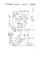
As previously mentioned, the DC component of the vertical sawtooth should be preserved and transmitted to the deflection yoke. DC coupling should be used between the sawtooth generator and the vertical amplifier (or modulator) as well as to the yoke coil. FIGS. 7 and 8 are detailed circuit diagram of a vertical scan generator having these features and having the constant retrace time (t0-t0', t1-T1' etc. of FIG. 4C) and the consistent reset level features important for achieving proper raster registration in the double field rate receiver of FIG. 1 which employs non-equidistant vertical sync pulses.
In FIG. 7 the sync pulse 2V' is applied to input 702 of a signal slicer comprising amplifier V1 based by resistors 704 and 706. Representative element values are shown for all components. The output of the slicer amplifier U1 is applied via resistor 708 to a pulse shaping circuit comprising amplifiers U2, U3 and V4 which generate a constant width reset pulse for triggering transistor Q1 of the ramp generator circuit 500 of FIG. 5. A hold control (variable 47K ohm resistor) in the pulse shaping circuit allows pulse width adjustment by varying the monostable period of the pulse "stretcher" formed by amplifier U2 and U3. Amplifier U4 inverts the conditioned pulses to provide the proper polarity drive signal for transistor Q1 of ramp generator 500.
In the vertical deflection circuit of FIG. 8 the ramp signal of FIG. 7 is DC biased by means of resistors 802-806 and buffered by amplifier U5. The output of amplifier U5 is applied to a linearity correction circuit (indicated generally as 808) which produces a smoothed linearity correction signal that is added to the ramp signal by means of resistors 810 and 812. Amplifier U7 applies the corrected sweep signal to the driver transistor 814 of the vertical output stage (indicated generally as 816). It will be noted from FIGS. 7 and 8 that DC coupling is used at every stage of the vertical processing from terminal 702 of the slicer of FIG. 7 to the yoke coil 818 in FIG. 8.

Claims (13)

What is claimed is:
1. A television display system, comprising:
input means for receiving an interlaced video input signal having a given field rate;
memory means coupled to said input means, said memory means having a write cycle for storing a field of said input signal and having first and second read cycles for recovering a previously stored field two times during said write cycle for providing a video output signal of double said given field rate;
display means coupled to said memory means for displaying said double field rate video output signal; and
timing means responsive to said video input signal for supplying a read control signal to said memory means for initiating said read cycles, said read control signal having a pulse waveform that repeats on a two-field basis, said timing means further supplying a vertical synchronizing signal to said display means having a pulse waveform that repeats on a four-field basis, each said pulse waveform having a nominal frequency of double said given field rate, said two-field and four-field pulse waveforms being selected to provide an image on said display means in which even fields overlay even fields, odd fields overlay odd fields and in which even and odd pairs of fields are interlaced.
2. A television display system as recited in claim 1 wherein said pulse waveform of said read control signal comprises pulses that are alternately spaced one-field minus one half-line apart and one field plus one-half line apart and wherein said pulse waveform of said vertical synchronizing signal comprises pulses having spacings therebetween which differ by multiples of one-half line from pulse-to-pulse such than no consecutive pair of pulses have the same spacing.
3. A television display system as recited in claim 1 wherein said memory means is responsive to said read control signal for providing said video output signal in which each field thereof includes a given number of active lines and in which every other field thereof also includes at least one blank line.
4. A television display system as recited in claim 1 further comprising scan generator means responsive to said vertical synchronizing signal for supplying a vertical scan signal to said display means of sawtooth form having a fixed starting point and a constant retrace time interval.
5. A television display system as recited in claim 1 wherein said video input signal is of PAL format, wherein said pulse waveform of said read control signal comprises pulses that are alternately spaced 312 and 313 lines apart and wherein said pulse waveform of said vertical synchronizing signal comprises consecutive pulses spaced apart by 312 lines, 312.5 lines, 312 lines and 313.5 lines in a repeating four-field sequence.
6. A television display system as recited in claim 1 wherein said timing means includes phase lock loop means responsive to a horizontal synchronizing component of said video input signal for providing a double line-rate output signal, divider means responsive to said double line rate output signal for providing a vertical rate output signal and phase detector means coupled to said counter means for synchronizing said vertical rate signal with a vertical synchronizing component of said video input means and decoder means coupled to said counter means for producing said double field rate pulse waveforms.
7. A division display apparatus as recited in claim 6 wherein said phase lock loop means includes controllable oscillator means having a given frequency control range and frequency multiplier means in said phase lock loop means for effectively increasing the control range of said controllable oscillator means.
8. A television display system, comprising:
input means for receiving an interlaced video input signal having a given field rate;
memory means coupled to said input means, said memory means having a write cycle for storing a field of said input signal and having first and second read cycles for recovering a previously stored field two times during said write cycle for providing a video output signal of double said given field rate;
display means coupled to said memory means for displaying said double field rate video output signal; and
timing means responsive to said video input signal for supplying a read control signal to said memory means for initiating said read cycles, said read control signal having a pulse waveform that repeats on a two-field basis selected such that each recovered field comprises a given number of active lines and every other field also includes at least one blank line, said timing means further supplying a vertical synchronizing signal to said display means having a pulse waveform that repeats on a four-field basis with no two consecutive pulses have the same spacing therebetween, said two-field and four-field pulse waveforms being selected to provide an image on said display means in which even fields overlay even fields, odd fields overlay odd fields and in which even and odd pairs of fields are interlaced.
9. A television display system as recited in claim 8 wherein said pulse waveform of said read control signal comprises pulses that are alternately spaced one-field minus one half-line apart and one-field plus one-half line apart and wherein said pulse waveform of said vertical synchronizing signal comprises pulses having a spacing therebetween which differ by a multiple of one-half line from pulse to pulse.
10. A television display system as recited in claim 8 wherein said video input signal is of PAL format, wherein said pulse waveform of said read control signal comprises pulses that are alternately spaced 312 and 313 lines apart and wherein said pulse waveform of said vertical synchronizing signal comprises consecutive pulses spaced apart by 312 lines, 312.5 lines, 312 lines, and 313.5 lines in a repeating four-field sequence.
11. A television display system as recited in claim 8 further comprising scan generator means responsive to said vertical synchronizing signal for supplying a vertical scan signal via a direct current coupled path to said display means said vertical scan signal being of sawtooth form having a fixed starting point and a constant retrace time interval.
12. A television display system as recited in claim 8 wherein said timing means includes phase lock loop means responsive to a horizontal synchronizing component of said video input signal for providing a double line-rate output signal, divider means responsive to said double line rate output signal for providing a vertical rate output signal and phase detector means coupled to said counter means for synchronizing said vertical rate signal with a vertical synchronizing component of said video input means and decoder means coupled to said counter means for producing said double field rate pulse waveforms.
13. A television display apparatus as recited in claim 12 wherein said phase lock loop means includes controllable oscillator menas having a given frequency control range and frequency multiplier means in said phase lock loop means for effectively increasing the control range of said controllable oscillator means.
US06/857,375 1986-04-11 1986-04-30 Television display system with flicker reduction processor Expired - Lifetime US4701793A (en)

Priority Applications (6)

Application Number Priority Date Filing Date Title
DE19873789396 DE3789396T2 (en) 1986-04-11 1987-04-09 Deflection device for a television set.
DE19873783255 DE3783255T2 (en) 1986-04-11 1987-04-09 TELEVISION PLAYBACK SYSTEM.
EP87303079A EP0241284B1 (en) 1986-04-11 1987-04-09 Television display system
EP19870303080 EP0242123B1 (en) 1986-04-11 1987-04-09 Television deflection apparatus
HK97101724A HK1000236A1 (en) 1986-04-11 1997-09-05 Television display system
HK98103033A HK1004047A1 (en) 1986-04-11 1998-04-14 Television deflection apparatus

Applications Claiming Priority (2)

Application Number Priority Date Filing Date Title
GB868608876A GB8608876D0 (en) 1986-04-11 1986-04-11 Television display system
GB8608876 1986-04-11

Publications (1)

Publication Number Publication Date
US4701793A true US4701793A (en) 1987-10-20

Family

ID=10596056

Family Applications (1)

Application Number Title Priority Date Filing Date
US06/857,375 Expired - Lifetime US4701793A (en) 1986-04-11 1986-04-30 Television display system with flicker reduction processor

Country Status (2)

Country Link
US (1) US4701793A (en)
GB (1) GB8608876D0 (en)

Cited By (22)

* Cited by examiner, † Cited by third party
Publication number Priority date Publication date Assignee Title
US4829380A (en) * 1987-12-09 1989-05-09 General Motors Corporation Video processor
US4851908A (en) * 1987-04-16 1989-07-25 U.S. Philips Corporation Field number doubling circuit for a television signal
EP0350765A1 (en) * 1988-07-12 1990-01-17 Deutsche Thomson-Brandt GmbH Transcoder
US5101273A (en) * 1989-08-04 1992-03-31 Laboratoire Europeen De Recherches Electroniques Advancees Societe En Nom Collectif Device for the conversion of motion information into a motion information signal at the field rate and with the number of lines desired for high-definition television
US5144445A (en) * 1989-12-26 1992-09-01 Sanyo Electric Co., Ltd. Solid-state image pickup apparatus having a plurality of photoelectric transducers arranged in a matrix
US5150214A (en) * 1989-07-29 1992-09-22 Samsung Electronics Co., Ltd. Method and circuit for correction of horizontal edges
US5182643A (en) * 1991-02-01 1993-01-26 Futscher Paul T Flicker reduction circuit for interlaced video images
US5247359A (en) * 1990-09-28 1993-09-21 Sharp Kabushiki Kaisha Field decision circuit for providing error free odd/even field information
US5469217A (en) * 1992-11-04 1995-11-21 U.S. Philips Corporation Arrangement for doubling the field frequency of a picture signal
US5485218A (en) * 1994-01-21 1996-01-16 Brother Kogyo Kabushiki Kaisha Image processor for producing even field video data based on odd field video data
US5627555A (en) * 1993-04-14 1997-05-06 Rca Thomson Licensing Corporation Line flicker suppression by adaptive de-interlacing
US5742270A (en) * 1996-03-06 1998-04-21 Industrial Technology Research Institute Over line scan method
US5844619A (en) * 1996-06-21 1998-12-01 Magma, Inc. Flicker elimination system
US5850263A (en) * 1994-10-05 1998-12-15 Sony Corporation Video signal processing apparatus for converting a frame video signal representing a plurality of video frames into a field signal representing a plurality of video fields
US5894330A (en) * 1997-01-23 1999-04-13 Silicon Integrated Systems Corp. Adaptive anti-flicker method for VGA to TV data conversion
US5986707A (en) * 1995-06-07 1999-11-16 Geshwind; David Michael Methods and devices for the creation of images employing variable-geometry pixels
US6054977A (en) * 1994-03-01 2000-04-25 Snell & Wilcox Limited Scanning converter for video display
US20010022612A1 (en) * 2000-03-16 2001-09-20 Fuji Photo Optical Co., Ltd. Electronic endoscope apparatus without flicker on screen
US6898327B1 (en) 2000-03-23 2005-05-24 International Business Machines Corporation Anti-flicker system for multi-plane graphics
US20110166968A1 (en) * 2010-01-06 2011-07-07 Richard Yin-Ching Houng System and method for activating display device feature
US20140340132A1 (en) * 2013-05-20 2014-11-20 Qualcomm Incorporated Method and apparatus for generating a reference signal for a fractional-n frequency synthesizer
CN108696702A (en) * 2017-03-31 2018-10-23 佳能株式会社 Device, system and mobile object

Citations (7)

* Cited by examiner, † Cited by third party
Publication number Priority date Publication date Assignee Title
US2681383A (en) * 1951-04-13 1954-06-15 Zenith Radio Corp Television receiver
US4322750A (en) * 1979-05-08 1982-03-30 British Broadcasting Corporation Television display system
US4426661A (en) * 1980-12-26 1984-01-17 Sony Corporation Television receiver including a circuit for doubling line scanning frequency
US4603351A (en) * 1984-09-05 1986-07-29 U.S. Philips Corporation Field-frequency doubling circuit
US4604651A (en) * 1982-12-07 1986-08-05 U.S. Philips Corporation Television circuit arrangement for field and line frequency doubling and picture part magnification
US4651209A (en) * 1983-11-07 1987-03-17 Sony Corporation Television display system with increased field frequency
US4658293A (en) * 1984-08-08 1987-04-14 Sanyo Electric Co., Ltd. Scanning conversion method and scan converter unit employing the conversion method

Patent Citations (7)

* Cited by examiner, † Cited by third party
Publication number Priority date Publication date Assignee Title
US2681383A (en) * 1951-04-13 1954-06-15 Zenith Radio Corp Television receiver
US4322750A (en) * 1979-05-08 1982-03-30 British Broadcasting Corporation Television display system
US4426661A (en) * 1980-12-26 1984-01-17 Sony Corporation Television receiver including a circuit for doubling line scanning frequency
US4604651A (en) * 1982-12-07 1986-08-05 U.S. Philips Corporation Television circuit arrangement for field and line frequency doubling and picture part magnification
US4651209A (en) * 1983-11-07 1987-03-17 Sony Corporation Television display system with increased field frequency
US4658293A (en) * 1984-08-08 1987-04-14 Sanyo Electric Co., Ltd. Scanning conversion method and scan converter unit employing the conversion method
US4603351A (en) * 1984-09-05 1986-07-29 U.S. Philips Corporation Field-frequency doubling circuit

Cited By (25)

* Cited by examiner, † Cited by third party
Publication number Priority date Publication date Assignee Title
US4851908A (en) * 1987-04-16 1989-07-25 U.S. Philips Corporation Field number doubling circuit for a television signal
US4829380A (en) * 1987-12-09 1989-05-09 General Motors Corporation Video processor
EP0350765A1 (en) * 1988-07-12 1990-01-17 Deutsche Thomson-Brandt GmbH Transcoder
US5150214A (en) * 1989-07-29 1992-09-22 Samsung Electronics Co., Ltd. Method and circuit for correction of horizontal edges
US5101273A (en) * 1989-08-04 1992-03-31 Laboratoire Europeen De Recherches Electroniques Advancees Societe En Nom Collectif Device for the conversion of motion information into a motion information signal at the field rate and with the number of lines desired for high-definition television
US5144445A (en) * 1989-12-26 1992-09-01 Sanyo Electric Co., Ltd. Solid-state image pickup apparatus having a plurality of photoelectric transducers arranged in a matrix
US5247359A (en) * 1990-09-28 1993-09-21 Sharp Kabushiki Kaisha Field decision circuit for providing error free odd/even field information
US5182643A (en) * 1991-02-01 1993-01-26 Futscher Paul T Flicker reduction circuit for interlaced video images
US5469217A (en) * 1992-11-04 1995-11-21 U.S. Philips Corporation Arrangement for doubling the field frequency of a picture signal
US5627555A (en) * 1993-04-14 1997-05-06 Rca Thomson Licensing Corporation Line flicker suppression by adaptive de-interlacing
US5485218A (en) * 1994-01-21 1996-01-16 Brother Kogyo Kabushiki Kaisha Image processor for producing even field video data based on odd field video data
US6054977A (en) * 1994-03-01 2000-04-25 Snell & Wilcox Limited Scanning converter for video display
US5850263A (en) * 1994-10-05 1998-12-15 Sony Corporation Video signal processing apparatus for converting a frame video signal representing a plurality of video frames into a field signal representing a plurality of video fields
US5986707A (en) * 1995-06-07 1999-11-16 Geshwind; David Michael Methods and devices for the creation of images employing variable-geometry pixels
US5742270A (en) * 1996-03-06 1998-04-21 Industrial Technology Research Institute Over line scan method
US5844619A (en) * 1996-06-21 1998-12-01 Magma, Inc. Flicker elimination system
US5894330A (en) * 1997-01-23 1999-04-13 Silicon Integrated Systems Corp. Adaptive anti-flicker method for VGA to TV data conversion
US20010022612A1 (en) * 2000-03-16 2001-09-20 Fuji Photo Optical Co., Ltd. Electronic endoscope apparatus without flicker on screen
US6898327B1 (en) 2000-03-23 2005-05-24 International Business Machines Corporation Anti-flicker system for multi-plane graphics
US20110166968A1 (en) * 2010-01-06 2011-07-07 Richard Yin-Ching Houng System and method for activating display device feature
US20140340132A1 (en) * 2013-05-20 2014-11-20 Qualcomm Incorporated Method and apparatus for generating a reference signal for a fractional-n frequency synthesizer
US8988121B2 (en) * 2013-05-20 2015-03-24 Qualcomm Incoporated Method and apparatus for generating a reference signal for a fractional-N frequency synthesizer
CN108696702A (en) * 2017-03-31 2018-10-23 佳能株式会社 Device, system and mobile object
US10812748B2 (en) * 2017-03-31 2020-10-20 Canon Kabushiki Kaisha Apparatus, system, and moving object
CN108696702B (en) * 2017-03-31 2021-06-29 佳能株式会社 Device, system and mobile object

Also Published As

Publication number Publication date
GB8608876D0 (en) 1986-05-14

Similar Documents

Publication Publication Date Title
US4701793A (en) Television display system with flicker reduction processor
EP0213912B1 (en) Video display system for wide and standard aspect ratio video signals
US6429904B2 (en) Method for converting analog video signal to digital video signal
US5812210A (en) Display apparatus
EP0229431B1 (en) Picture-in-picture color television receiver
EP0551168B1 (en) Display apparatus
EP0213911B1 (en) Compatible wide screen television system
KR950014577B1 (en) Pip signal control method & apparatus of hdtv
JP2502829B2 (en) Image display device
JPS58151781A (en) Convertible wide screen television device
US4521802A (en) Double-scanning non-interlace color television receiver
US4595953A (en) Television receiver having character generator with burst locked pixel clock and correction for non-standard video signals
US5896177A (en) Device for controlling an aspect ratio in tv-monitor integrated wide screen receiver
EP0241284B1 (en) Television display system
GB2168219A (en) Progressive scan television system
US20020030759A1 (en) Display device also compatible with digital broadcasts
JPH0547025B2 (en)
US4782269A (en) Sawtooth generator with s-correction
GB2050729A (en) Television horizontal afpc systems
US4737691A (en) Television apparatus for generating a phase modulated deflection current
EP0242123B1 (en) Television deflection apparatus
KR0182066B1 (en) Image signal transformation apparatus of digital formation
JP2525431B2 (en) RGB multi-terminal input type progressive scan conversion television receiver
JPS595781A (en) Horizontal scanning system
JP3550302B2 (en) Reciprocating deflection type video signal display

Legal Events

Date Code Title Description
AS Assignment

Owner name: RCA CORPORATION, A CORP. OF DE.

Free format text: ASSIGNMENT OF ASSIGNORS INTEREST.;ASSIGNORS:DEN HOLLANDER, WILLEM;LEONARDI, GIOVANNI M.;REEL/FRAME:004564/0071

Effective date: 19860527

STCF Information on status: patent grant

Free format text: PATENTED CASE

AS Assignment

Owner name: RCA LICENSING CORPORATION, TWO INDEPENDENCE WAY, P

Free format text: ASSIGNMENT OF ASSIGNORS INTEREST.;ASSIGNOR:RCA CORPORATION, A CORP. OF DE;REEL/FRAME:004993/0131

Effective date: 19871208

FPAY Fee payment

Year of fee payment: 4

FPAY Fee payment

Year of fee payment: 8

FPAY Fee payment

Year of fee payment: 12