US4714536A - Planar magnetron sputtering device with combined circumferential and radial movement of magnetic fields - Google Patents

Planar magnetron sputtering device with combined circumferential and radial movement of magnetic fields Download PDF

Info

Publication number
US4714536A
US4714536A US07/032,916 US3291687A US4714536A US 4714536 A US4714536 A US 4714536A US 3291687 A US3291687 A US 3291687A US 4714536 A US4714536 A US 4714536A
Authority
US
United States
Prior art keywords
target
magnetic
assembly
axis
magnetic field
Prior art date
Legal status (The legal status is an assumption and is not a legal conclusion. Google has not performed a legal analysis and makes no representation as to the accuracy of the status listed.)
Expired - Fee Related
Application number
US07/032,916
Inventor
Kenneth F. Freeman
Charles B. Garrett
David J. Harra
Lawrence C. Lei
Current Assignee (The listed assignees may be inaccurate. Google has not performed a legal analysis and makes no representation or warranty as to the accuracy of the list.)
Novellus Systems Inc
Original Assignee
Varian Associates Inc
Priority date (The priority date is an assumption and is not a legal conclusion. Google has not performed a legal analysis and makes no representation as to the accuracy of the date listed.)
Filing date
Publication date
Application filed by Varian Associates Inc filed Critical Varian Associates Inc
Priority to US07/032,916 priority Critical patent/US4714536A/en
Application granted granted Critical
Publication of US4714536A publication Critical patent/US4714536A/en
Assigned to NOVELLUS SYSTEMS, INC. reassignment NOVELLUS SYSTEMS, INC. ASSIGNMENT OF ASSIGNORS INTEREST (SEE DOCUMENT FOR DETAILS). Assignors: VARIAN ASSOCIATES, INC.
Anticipated expiration legal-status Critical
Expired - Fee Related legal-status Critical Current

Links

Images

Classifications

    • HELECTRICITY
    • H01ELECTRIC ELEMENTS
    • H01JELECTRIC DISCHARGE TUBES OR DISCHARGE LAMPS
    • H01J37/00Discharge tubes with provision for introducing objects or material to be exposed to the discharge, e.g. for the purpose of examination or processing thereof
    • H01J37/32Gas-filled discharge tubes
    • H01J37/34Gas-filled discharge tubes operating with cathodic sputtering
    • H01J37/3411Constructional aspects of the reactor
    • H01J37/345Magnet arrangements in particular for cathodic sputtering apparatus
    • H01J37/3455Movable magnets
    • HELECTRICITY
    • H01ELECTRIC ELEMENTS
    • H01JELECTRIC DISCHARGE TUBES OR DISCHARGE LAMPS
    • H01J37/00Discharge tubes with provision for introducing objects or material to be exposed to the discharge, e.g. for the purpose of examination or processing thereof
    • H01J37/32Gas-filled discharge tubes
    • H01J37/34Gas-filled discharge tubes operating with cathodic sputtering
    • H01J37/3402Gas-filled discharge tubes operating with cathodic sputtering using supplementary magnetic fields
    • H01J37/3405Magnetron sputtering
    • H01J37/3408Planar magnetron sputtering

Landscapes

  • Physics & Mathematics (AREA)
  • Engineering & Computer Science (AREA)
  • Plasma & Fusion (AREA)
  • Chemical & Material Sciences (AREA)
  • Analytical Chemistry (AREA)
  • Physical Vapour Deposition (AREA)

Abstract

A planar magnetron sputtering device has an extended flat circular target source in opposed spaced parallel relationship with a generally flat article to be coated, placed within an evacuated coating chamber. Crossed electric and magnetic fields in the chamber are established in order to set up a plasma adjacent the target. The magnetic field is provided by a magnetic assembly of permanent magnets on the non-vacuum side of the target. The magnetic assembly is smaller in diameter than the target, but is mounted to a means for moving the assembly laterally over the entire area of the target. This means for moving sweeps the magnetic assembly in an eccentric path generally centered on the target center, with the path being non-reentrant and precessing about the target center with time. In this manner, the path sweeps different areas on successive rotations about the center, and a given area of target is exposed to the magnetic field at many successively different orientations. Articles are therefore coated with significantly improved uniformity and step coverage, while utilization of target material is improved.

Description

This application is a continuation of application Ser. No. 769,232, filed Aug. 26, 1985.
FIELD OF INVENTION
This invention relates to devices generating a plasma by establishing crossed electric and magnetic fields in a low pressure atmosphere of inert gas, for causing coating material to be removed from a target and deposited on an article to be coated; or for etching such an article. More particularly, this invention relates to devices of the foregoing type in which coatings are deposited (or material removed), specifically by sputtering, as in planar magnetron sputtering devices; plasma-assisted chemical vapor deposition; or by etching; and in which the magnetic field is moved during such coating or etching.
DESCRIPTION OF THE PRIOR ART
The coating of articles by sputtering, as well as the related process of removal of surface material by etching, are well established arts. Both require establishing an environment in which ions bombard a surface from which material is sought to be removed; allowing the particles thus removed to condense on another surface which is to be coated. The ions result from a plasma created by establishing crossed magnetic and electrical fields in a low pressure atmosphere of inert gas, as for example within a processing or coating chamber.
In the case of a typical sputter coating application, an article to be coated, typically having an extended generally flat surface, is positioned within the processing chamber in spaced opposing relationship to a flat target material, which also preferably has an extended flat surface, and which is attached to one wall of the chamber but is insulated therefrom. The target is subjected to a DC or RF voltage, and acts as a cathode, while the walls of the chamber and the article to be coated may be at ground potential. An electric field is thus established in the space between the elements of the chamber at ground potential, and the cathode-target. Outside the chamber, adjacent the wall to which is attached the target, a magnetic assembly establishes magnetic lines of force which pass through the target and, over a part of their path, are parallel with the surface thereof which is to be coated, as well as in crossed relationship to the electric field lines of force. Ions from the plasma bombard the target and erode material therefrom, and at least a part of the particles of material emanating from the target then accumulate on the surface of the article to be coated.
In the case of RF sputter etching of articles having flat surfaces, such as semiconductor wafers, an RF potential is applied to the article, while the target and other surrounding surfaces are at ground potential. The RF plasma then causes material to be eroded from the article, thus etching same.
A characteristic of sputtering and other comparable processes is a tendency for the target material to be eroded nonuniformly, so that it must be replaced more frequently because of localized erosion, despite the fact that the remainder of the target may not exhibit much wear. If such a localized erosion can be minimized, and the target material utilized more uniformly, material and fabrication expenses can be greatly reduced.
Another even more important consideration is that coating materials be deposited over the article to be coated in a uniform fashion. A principal application of sputter coating is to the processing of semiconductor wafers which are to be made into integrated circuits. Because of the extreme number of identical individual circuits, commonly called "chips", which are created from a single semiconductor wafer, of typically four to six inches in diameter, tolerances in the permissible variations in coating coverage along the surface area are extremely rigorous, and are becoming even more exacting as newer generation products, with even more densely packed active elements, are developed with time.
Many variations in sputtering techniques and devices have been employed in a continuing effort to achieve both satisfactory lifetime for expensive target material assemblies, and a satisfactory level of coating uniformity. One very useful technique has been to cause the magnetic assembly to be moved relative to the target, so as to erode the target more uniformly. One example of this technique is found in U.S. Pat. No. 4,444,643. In this patent, a subassembly comprising an array of permanent magnets is swept laterally across the non-vacuum side of a flat target of larger size, either in a circular motion, or in a linear transverse motion. In one embodiment, the target is in the form of a flat disk, with the magnet assembly in the form of a smaller disk mounted off center to a drive shaft coinciding with the axis of the target disk. In another embodiment, the target is a rectangular plate, with the magnet assembly being translated over a linear path back and forth to sweep the area of the target.
Another prior art device, described in the published German Patent Application Ser. No. P2707144.9, filed Feb. 17, 1977, and claiming the priority of U.S. patent application Ser. No. 659,270 filed Feb. 19, 1976 to John F. Corbani, relies on much the same principles as in the foregoing patent. The target is a flat plate, and a magnet assembly is swept over a surface of the chamber immediately opposite the target plate along a linear path.
The foregoing arrangements, while representing a considerable improvement over devices with a fixed magnet to target relationship, still have fallen well short of consistently providing the level of quality and uniformity of coating necessary for today's coating requirements, not to mention the greater demands already foreseen for future higher density devices now under development. Because of the cost of materials, which may include even gold, utilized as targets, not to mention manufacturing costs in purifying and fabricating same into complete cathode assemblies, even the early advantages of the foregoing arrangements in combating uneven erosion of target surfaces have not proven fully satisfactory. Nor have the prior devices been able to provide a fully satisfactory combination of both uniformity of coating and satisfactory evenness of target erosion.
SUMMARY OF THE INVENTION
Accordingly, an object of the invention is to provide a crossed field plasma discharge device for depositing a coating on an object with a hitherto unobtainable degree of uniformity; or to uniformly etch the surface of an article.
It is also an object of the invention to provide a crossed field plasma discharge device which utilizes target material evenly while also providing a superior degree of uniformity in coating an article, at all stages of target life.
It is a further object of the invention to provide relative movement between the target and the magnetic field in an improved manner resulting in superior coating performance and target longevity.
It is a particular object of the invention to provide an improved mechanism of greater reliability and comparative simplicity while yet providing clearly improved sweep coverage of the target by the magnetic field.
It is a more particular object of the invention to sweep the target with a magnetic field which maintains a parallel component and an even distance to the surface of a flat target while otherwise varying in orientation and location relative thereto to a much greater degree than previously.
It is another particular object of the invention to provide a means of easily adjusting the relative movement between target and magnetic field to accommodate a wide range of workpiece dimensions and target materials.
According to the present invention, these and other objects and advantages are achieved in a device for generating a plasma by use of crossed electrical and magnetic fields. The device comprises means for forming an electrical field, means for forming a magnetic field intersecting the electrical field, and magnetic field movement means for moving the magnetic field around the first axis at a first radial distance therefrom while causing the magnetic field to move radially with respect to the first axis during movement around the first axis.
BRIEF DESCRIPTION OF THE DRAWINGS
For a better understanding of the present invention together with other and further objects, advantages, and capabilities thereof, reference may be had to the accompanying drawings which are incorporated herein by reference and in which:
FIG. 1 is a cross-sectional view of a sputtering device in accordance with the present invention;
FIG. 2 is a top view of the magnet rotor assembly taken through the line 2--2 of FIG. 1;
FIG. 3 is a bottom view of the magnet rotor assembly taken through the line 3--3 of FIG. 1;
FIG. 4 is a cross-sectional view of the magnet rotor assembly taken through the line 4--4 of FIG. 2;
FIG. 5 is a simplified bottom view of the magnet assembly taken through the line 5--5 of FIG. 4;
FIG. 6 illustrates the movements of the various elements of the rotor assembly shown in FIGS. 1-4; and
FIGS. 7-9 illustrate movement of the magnet assembly in relation to the target.
DETAILED DESCRIPTION OF THE INVENTION
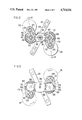
A crossed field sputtering device in accordance with the present invention is illustrated in FIG. 1. A workpiece support 10 is positioned in a sputtering chamber 11 enclosed by a chamber housing 12 which can be evacuated by suitable vacuum pumping means (not shown) and can be backfilled with a suitable gas such as argon. Typically, means for exchanging wafers automatically is also provided. A workpiece 14, typically a semiconductor wafer having a diameter typically of 150 mm (though larger or smaller diameters can be accommodated) can be positioned on the workpiece support 10 and exchanged by automatic wafer exchanger means (not shown). Mounted at one end of the sputtering chamber 11 facing the workpiece 14, is a target assembly 16 comprising a sputtering target 18 and a target backing plate 20. The sputtering target 18 is fabricated of the material to be deposited on the workpiece 14 and is soldered to the target backing plate 20. Surrounding the workpiece support 10 and the workpiece 14 is an annular confinement shield 22 attached to a shield support 24, which is mounted to the chamber housing 12. The target backing plate 20 is provided with a flange 30 for mounting of the target assembly 16 to the chamber housing 12. The target assembly 16 and chamber housing 12 are electrically isolated by an insulator 32. Mounted on the target assembly 16 external to the sputtering chamber 11 are an annular lower housing 36 and a generally plate-like upper housing 38. The target assembly 16, the lower housing 36, and the upper housing 38 enclose a chamber 40 which contains a magnet assembly 42.
The device shown in FIG. 1 also includes means for establishing relative lateral motion between the magnet assembly 42 and the target 18. The magnet assembly 42 and the means for moving the magnet assembly 42 are described in detail hereinafter. It will be understood that the sputtering chamber 11 and the chamber 40 are isolated from each other. During operation of the sputtering device of FIG. 1, considerable heating of the target assembly 16 takes place. A liquid is typically circulated through the chamber 40 for heat removal. The liquid can be circulated through coolant hoses 44, 46 which pass through the upper housing 38 and connect to a cooling system (not shown).
In operation, a workpiece 14 is introduced into the sputtering chamber 11 on the workpiece support 10. The chamber 11 is sealed and evacuated. A background gas, such as argon may be introduced. In order to initiate sputtering, an electric field is established in the sputtering chamber 11 by application of a voltage between the target assembly 16 and the workpiece 14. Typically, the workpiece 14 is grounded (or maintained at a base DC or RF potential) and a DC or an RF voltage is applied to the target assembly 16 (Also chamber housing 12, shield 22, and shield support 24 are typically grounded). As a result, an electric field perpendicular to the target 18 and the workpiece 14 surfaces is established in the sputtering chamber 11. The magnet assembly 42 contains permanent magnets which establish magnetic fields, (illustrated by magnetic field line 48) as shown in FIG. 1, which have segments generally parallel to the target 18 surface and perpendicular to the electric field. A plasma is established in the sputtering chamber 11 in the region between the target 18 and the workpiece 14 where the electric and magnetic fields are crossed. Ions in the plasma bombard the target 18 surface and cause sputtering of the target material, some of which is deposited on the surface of the workpiece 14.
It is necessary that the material sputtered from the target 18 be deposited on the surface of workpiece 14 with high uniformity over the surface area of the workpiece 14. It is also desirable that the material be uniformly eroded from the surface of the target 18 since a small area with severe erosion necessitates more frequent replacement of the entire target at a substantial cost. The prior art system shown in U.S. Pat. No. 4,444,643 uses a magnet assembly which is rotated around an axis coincident with the centers of the target and the workpiece. This arrangement has the advantage that the magnet assembly moves over the target surface in a uniform fashion, resulting in more uniform erosion of the target material than prior expedients. In addition, the target material is directed at the workpiece from a variety of directions, thereby improving deposition uniformity.
However, one disadvantage of this arrangement is that a fixed point on the magnet assembly always rotates over a given radial position on the target, producing a given magnetic field strength and direction. At a different radial position on the target, a second magnetic field strength and direction is produced. However, the field strengths and directions at the different radial positions are not necessarily the same. As a result, there is a tendency for sputtering rate variations in the radial direction and consequent circular thickness variations on the target surface. It can be seen that the same effect can produce radial variations in the film deposited on the workpiece.
The present invention overcomes the above disadvantages by providing a magnet assembly which is rotated about a central axis relative to the target surface and is simultaneously rotated about a second axis spaced from the central axis, the magnet assembly being mounted off-center with respect to the second axis. The magnet assembly is moved laterally in a plane parallel to the plane of the target on the side of the target opposite that which faces the workpiece. The magnet assembly is moved relative to the target in a predetermined pattern wherein substantially the entire area of the target is traversed. The pattern is essentially an epicycloid which is displaced about the axis of rotation with each successive revolution, the effect of which is a precession or rotation of the pattern about the central axis. After a given number of rotations about the central axis, the entire area of the target is substantially uniformly traversed. The pattern traced by the magnet assembly can be predetermined by appropriate choice of the various gear ratios, rotation rates, diameters, etc. in order to achieve a given sputtered film uniformity and target erosion rate.
A preferred embodiment of the present invention for establishing lateral motion of the magnet assembly 42 is illustrated in FIG. 1-4. The means for moving the magnet assembly 42 includes a magnet rotor assembly 50, a rotor shaft assembly 52, a drive assembly 54, and a motor assembly 56. The entire assembly is shown in FIG. 1, while the magnet rotor assembly is illustrated in detail in FIGS. 2-4. The magnet rotor assembly 50 rotates about the rotor shaft assembly 52 when driven by the motor assembly 56 through the drive assembly 54. The rotor shafy assembly 52 includes a fixed shaft 60 rigidly attached at one end to an upwardly extending post 62 in the center of the target backing plate 20. The other end of the fixed shaft 60 is attached to the upper housing 38 by means of a center support flange 64. The rotor shaft assembly 52 also includes a fixed gear 66 and a gear spacer 68, both rigidly attached to the shaft 60 and concentric with the shaft 60 and positioned at the top of the hub post 62.
The motor assembly 56 includes a motor 76 mounted to a motor bracket 78 which is fixedly attached to the upper housing 38. A motor mitre gear 80 is positioned on the drive shaft of the motor 76.
The drive assembly 54 includes a drive shaft 84 positioned for rotation in bearings 86 carried in a drive hub 88 rigidly attached to the upper housing 38. A drive shaft mitre gear 90 is attached to one end of the drive shaft 84 and positioned to mesh with the motor mitre gear 80. A drive gear 92 is mounted at the opposite end of the drive shaft 84 and mates with a driven gear 94 on the rotor assembly 50. The rotor assembly 50 is caused to rotate at an angular velocity determined by the speed of the motor 76 and the gear ratios of the mitre gears 80, 90, the drive gear 92 and the driven gear 94. A cover 95 shields the operator from the mitre gears 80, 90, and the target voltage on shaft 84. A seal 201 prevents coolant from leaking out of chamber to around shaft 84.
The rotor assembly 50 includes a rotor hub 96 which rotates about the fixed shaft 60 on bearings 98. The rotor assembly 50 is provided with idler shafts 100 which are symmetrically located on opposite sides of the rotor hub 96 with respect to the shaft 60 and which are mounted in bearings 102 so as to permit rotation with respect to the rotor hub 96. Attached to the idler shafts 100 are idler gears 104, each having teeth which mesh with the teeth of the fixed gear 66. When the rotor hub 96 rotates about the fixed shaft 60, the gear 66 remains fixed in position, causing rotation of the idler gears 104.
The rotor assembly 50 is further provided with oscillator arms 106 attached to the ends of the rotor hub 96. In the embodiment of FIGS. 1-4, the oscillator arms 106 are attached to the rotor hub 96 by means of mounting hardware 108 through slotted holes 110 for adjustability, to accommodate workpieces of different sizes and different target materials. Adjustment of the rotor hub 96 on the oscillator arm 106 determines the value R1 in FIG. 6, whose significance will be discussed below. It will be understood that the oscillator arms 106 can be mounted in fixed positions or can simply be constructed as extensions of the rotor hub 70. Positioned near the end of the oscillator arms 104 are oscillator shafts 120 mounted with bearings 122 to permit rotation with respect to the idler gears 104. Mounted on the oscillator shafts 120 are oscillator gears 124, located for rotation by idler gears 104. The magnet assembly 42 is attached to one of the oscillator gears 124 through a spacer 126. The magnet assembly 42 is positioned off-center with respect to the oscillator shaft 120. Attached to the other oscillator gear 124 at the opposite end of the rotor hub 96 is a counterweight 128, having a similar size and weight to the magnet assembly 42. The purpose of the counterweight 128 is to provide balanced rotation of the rotor assembly 50. Alternatively, a second magnet assembly can be connected to the opposite end of the rotor assembly 50.
The magnet rotor assembly 50 is also provided with a magnet support arm 130, mounted to the central portion of the rotor hub 96, and angularly displaced from the idler gear 104 and oscillator arm 106, as shown in FIGS. 2 and 3. Attached near the ends of the magnet support arm 130 are permanent magnets 132 used for rotation sensing. A rotation sensor 134 is mounted in the upper housing 38 in alignment with the permanent magnets 132. Each time a magnet 132 passes the rotation sensor 134, a rotation indicating signal is generated for use by associated control apparatus (not shown). It will be understood that any convenient type of rotation sensing device, such as optical or capacitive, can also be utilized.
The magnet assembly 42 is shown in more detail in FIGS. 4 and 5. Permanent magnets 140 are mounted in a circular cup-shaped holder 142. The magnets 140 are each mounted with the north-south axis aligned with a radius of the cup-shaped holder 142, such that north poles of each magnet 140 are adjacent the center of the holder 142 and south poles are adjacent the periphery. Other magnet configurations can be utilized, as shown in U.S. Pat. No. 4,444,643. However, generally the permanent magnets are mounted on radii of a circle.
Operation of the motor 76 causes rotation of the drive shaft 84 and the drive gear 92. The driven gear 94 and attached rotor hub 96 are caused to rotate about the fixed shaft 60 (also defining the central axis of target 18). Referring now to FIG. 3, it can be seen that as the rotor hub 96 rotates about the shaft 60, the idler gears 104 rotate because the gear 66 is fixed in relation to the shaft 60 and does not rotate. Rotation of the idler gears 104 in turn causes rotation of the oscillator gears 124 and the attached magnet assembly 42. The magnet assembly 42 is mounted eccentrically with respect to the oscillator shaft 120 by a distance R2, as illustrated and explained in detail in connection with FIG. 6. In operation, the entire rotor assembly 50 carried by the rotor hub 96 rotates about the shaft 60 and the magnet assembly 42 simultaneously rotates around the oscillator shaft 120.
The resultant motion depends in detail on the parameters of the rotor assembly, such as gear ratios and radii. The magnet assembly 42 moves laterally in a plane parallel to the target 18 in a generally circular fashion. At any instant of time, the motion of the magnet assembly 42 which results in more uniform coverage of the target can be broken down into a circumferential component and a radial component 18, i.e., or into circular movement about the central axis of target 18, plus radial movement with respect to the central axis; or into two circular components, as mentioned above. A single rotation of the magnet assembly 42 about the central axis 60 of the target 18, including the combination of both circumferential and radial motion, is illustrated generally in FIG. 7. It may be seen that the resultant motion defines an eccentric path 45 of the magnet assembly 42 over target 18. (For purposes of illustrating the path 45 with more emphasis note that the diameter of target 18 has been exaggerated, while the diameter of assembly 42 is shown as smaller in proportion to target 18 than its actual proportions). A magnet assembly path 45 such as shown in FIG. 7 can be designed by proper choice of the gear ratio to rotate about the central axix 60. Thus, over a period of time, the path 42 precesses, moving over some new areas of target 18, while overlapping other previously-swept areas of target at successively different angles of attack, sweeping out a cycloidal pattern over time, and resulting in uniform tracing of the target area during successive rotations. As a result, the magnet assembly 42 is successively moved over substantially the entire surface area of the target 18. In addition, the magnet assembly and its magnetic field are placed in different orientations with respect to each point on the target surface. Thus sputtering occurs from essentially the entire target surface, and material is deposited on the workpiece from a variety of directions due to the various field orientations. Uniform erosion of the target 18 and uniform deposition of the target material on the workpiece 14 are thereby promoted.
The resultant eccentric motion of the magnet assembly 42 about central axis 60 can also be analyzed into combinations or various other simultaneous motions, for example, of one larger diameter circular motion at a first radial distance R1 about central axis 60, and a second circular motion about a smaller radial distance R2, and centered on a circular locus at a distance R1 from the central axis. FIG. 6 best illustrates this analysis of the motion of assembly 42. Again, illustrated in outline form are fixed gear 66, whose axis coincides with central axis 60; idler gears 104; oscillator gears 124; and magnetic assembly 42 mounted to one of oscillator gears 124; and counterweight 128 mounted similarly to the other of the oscillator gears. As previously noted, magnet assembly 42 is mounted off center with respect to the central axis and shaft of oscillator gear 124. This offset distance between the respective centers of assembly 42, and the oscillator gear is of course the smaller radial distance R2 in FIG. 6.
It will then be appreciated that a resultant radius R will be defined, extending between central axis 60 and the center of magnet assembly 42; this resultant radius can be seen to be the third leg of a triangle whose smaller first legs are R1 and R2, and which subtend therebetween the angle theta. This radius R is of course the radius of the locus of the center of the magnet assembly 42 as it moves about the central axis 60, in a movement resulting from the combination of the larger circular motion at radius R1 and the smaller circular offset motion of radius R2. One example of such a locus or path 45 of the center of assembly 42 is that of FIG. 7. In this preferred example, the path is generally egg-shaped, or more properly cycloidal, since it is not retraced in each successive revolution around axis 60. Rather, path 45 precesses, to a degree controlled by the choice of gear ratios and relative rotation speeds, so that a new area of the target is included during each successive sweep, while previously swept points on the target are again swept, but at angles differing from those of the previous sweeps.
As noted above, the particular path traced by the magnet assembly 42 depends on the radii and gear ratios of the rotor assembly 50. Since the magnet assembly 42 is a rigid unit, consideration of the motion of one point thereon is representative of the motion of the assembly. One further helpful way of analyzing the manner in which the pattern such as that of FIG. 7 traced is by comparison of the rate of rotation Wr of the rotor hub 96 and the rate of oscillation W0 of the magnet assembly 42 about the oscillator shaft 120. Simplified examples for purposes of this analysis of possible magnet paths are given in FIGS. 8 and 9. FIG. 8 illustrates the motion of a point M on the magnet assembly 42 for the case where Wr=W0; that is, for every rotation of the rotor hub 96, the magnet assembly 42 makes one complete rotation about the oscillator shaft 120. The dashed circles in FIG. 8 represent the inner and outer limits of motion of the point M on the magnet assembly 42. FIG. 9 illustrates the case where W0=4 Wr; that is, the magnet assembly 42 rotates about the oscillator shaft 120 four times for each complete rotation of the rotor hub 96 about the shaft 60. It can be seen from FIG. 9 that the motion is epicycloid in character.
The pattern shown in FIG. 8 is repetitive since it begins and ends at point A. Similarly, the pattern shown in FIG. 9 is repetitive since it starts and ends at point B. Repetitive patterns are undersirable in obtaining uniform target erosion and uniform film deposition since they repetitively trace the same patterns and will cause a pattern of non-uniform erosion grooves in the target. Such repetitive pattersn are avoided in the present invention by causing the patterns to rotate about the axis 60 by proper selection of the gear ratios in the rotor assembly 50. For example, with reference to FIG. 8, the pattern can be made to rotate about the axis 60 by establishing gear ratios wherein W0 is slightly greater or slightly less than Wr. The pattern then begins at point A but ends at point A' or A". Thus the second rotation about the axis 60 starts at A' or A" and is displaced from the first. Similarly, successive rotations will be displaced around the target area. Similarly, when W0 is slightly greater or slightly less than 4Wr, the pattern shown in FIG. 9 is displaced during each successive rotation. In this manner it may be seen that a pattern such as that of FIG. 7 is produced which does not repeat itself on each successive rotation, but rather constantly includes new areas, while changing its orientation with respect to the previous sweep path when overlapping previously swept areas.
The patterns shown in FIGS. 7, 8 and 9 are but examples of a large number of patterns which can be employed in accordance with the present invention. In order that the patterns be displaced on successive rotations rather than repetitively tracing the same path, W0 is made unequal to nWr where n is an integer. The spacing between successive patterns can also be determined by the relative values of W0 and Wr. Generally it is desirable to have successive patterns spaced by a dimension less than the dimension of the magnet assembly so that there are no gaps in the coverage of the target surface. A further consideration in selecting the pattern to be traced is that the entire target surface should be traversed by the magnet assembly one or more complete times during the deposition time of a workpiece in order to insure uniform film deposition. The pattern of magnet coverage during deposition can be adjusted to some extent by varying the speed of rotation of the magnet assembly about the central axis 60. A further consideration is that the inner and outer radial limits of magnet assembly travel, as determined by the size and eccentric mounting position of the magnet assembly, and the adjustment of rotor hub 96 on oscillator arm 106, should correspond generally with the target dimensions, object dimension and target material.
In a preferred embodiment of the present invention, very high uniformity was achieved in coating aluminum onto such thin generally circular workpieces 14 as typical semiconductor wafers commonly used in the industry to fabricate integrated circuits. Sputtering target 18 had a diameter nearly twice that of the workpiece, and had a composition of nearly pure aluminum with 1% silicon. A spacing between workpiece 14 and target 18 was established of somewhat less than 1/3 of the workpiece diameter. Magnet assembly 42 was of a diameter somewhat greater than 1/2 that of workpiece 14. Radius R1 was somewhat greater than 1/2 that of workpiece 14 (but less than the diameter of magnet assembly 42). Offset radius R2 was somewhat greater than 1/4 of R1. An inventive system in accordance with the above has achieved, on a 150 millimeter wafer, a uniformity of coating of at least ±4.5% (excluding the outer few millimeters of the workpiece radius). Moreover, each given location on the workpiece has received deposited material from so many different angles due to the many variations in the position of magnetic field to which the location has been exposed during successive rotations of magnet assembly 42. Thus coating coverage in the main plane of a flat workpiece not only has superior uniformity, but also any irregularities or steps in the workpiece also will be coated much more uniformly than in the prior art.

Claims (32)

I claim:
1. A crossed field sputtering device for sputtering material on a planar substrate:
a source of coating material having a target surface;
means for locating a planar substrate to be coated in a first position spaced from and facing said target surface;
means for establishing an electrical field in the space between said means for locating a substrate to be coated and said target surface;
magnetic means on the side of said source opposite said substrate locating means, said magnetic means forming a magnetic field in said space intersecting said electrical field; and
means for establishing relative lateral epicycloidal motion between said magnetic means and said target surface, said epicycloidal motion of said magnetic means occurring in a plane parallel to said target surface, said epicycloidal motion changing steadily with time, so that said magnetic means traverses a steadily changing area of said target surface whereby coating material is uniformly sputtered upon a surface of a substrate to be coated while said target surface is eroded relatively uniformly.
2. The device of claim 1 in which said electric field is a radio frequency field.
3. The device of claim 1 in which said electric field is a DC field.
4. The device of claim 1 in which said target surface is a flat one, and said magnetic means defines magnetic dipoles oriented in directions parallel to said target surface.
5. The device of claim 1 in which said means for establishing relative motion imparts a first motion in which said magnetic means rotates off center in a pattern sweeping a small fraction of said target surface.
6. The device of claim 5 in which said means for establishing relative motion imparts a second motion component in which said magnet means also simultaneously moves in an eccentric path over a substantial fraction of the area of said target surface.
7. The device of claim 6 in which said eccentric path shifts in orientation with respect to the target surface with time.
8. The device of claim 7 in which said eccentric path is cycloidal with time.
9. The device of claim 1 in which said means for establishing epicycloidal motion imparts a first motion to said magnetic means to rotate the same about a first axis at a first radial distance which is small relative to the lateral dimensions of said target surface.
10. A device as in claim 9 in which said means for establishing epicycloidal motion imparts a second motion to said magnetic means to rotate said first axis about a second axis at a second radial distance larger than said first radial distance.
11. A device as in claim 10 in which said magnetic means is generally circular, with magnetic dipoles directed radially, and in which said target surface is generally circular, the target radius being larger than the diameter of said magnetic means, and in which said second radial distance is smaller than the radius of said target.
12. A planar magnetron sputtering device in which a target source of coating material and a substrate to be coated are located in opposed spaced relationship in an evacuated chamber, and an electric field is established in the space between said target and said substrate, the improvement in which:
said target source of coating material is of planar disk-shaped configuration with a substantially flat target surface and a central axis, and which includes
means for positioning a substrate having a surface to be coated in a first location in which said surface faces said target;
a magnetic assembly on the side of said target source opposite said substrate positioning means, said assembly having lateral dimensions which are a fraction of the radius of said target surface;
and means for moving said magnetic assembly laterally within a plane parallel to and adjacent said target surface along an epicycloidal path generally centered on said central axis, said path being rotated about said axis with time.
13. The device of claim 12 in which said means for moving said magnetic assembly imparts to said assembly a first circular motion centered on said target central axis, with a first radius less than that of said target surface, and a second circular motion centered on an auxiliary axis located on a circular locus at said first radius, said second motion having a second radius which is less than said first radius.
14. The device of claim 12 in which said magnetic assembly is generally disk-like, defines magnetic dipoles in radial directions, is parallel to said flat target surface, and has a radius which is less than that of said target surface.
15. The device of claim 12 in which said magnetic assembly sweeps over said target surface in an eccentric path centered on said central target axis, said eccentric path rotating about said central axis so that said assembly is moving over said eccentric path sweeps different but overlapping areas of said target surface with time.
16. A device as in claim 15 in which said magnetic assembly defines an assembly central axis, said means for moving said assembly imparting a motion of rotation about said assembly central axis while moving said assembly over said eccentric path.
17. In a device for generating a plasma by use of crossed electrical and magnetic fields:
means for forming an electrical field;
magnetic means for forming a magnetic field intersecting said electrical field;
magnetic field movement means for moving said magnetic field around a first axis at a first radial distance therefrom, while causing said magnetic field to move radially with respect to said first axis during movement around said first axis in an epicycloidal path.
18. The device of claim 17 in which said means for forming a magnetic field is a magnetic assembly of symmetric geometry defining a center, and which is mounted off center to said means for rotating said magnetic field around said first axis, whereby said means for moving said magnetic field causes said magnetic assembly to execute cycloidal motion about said first axis.
19. The device of claim 17 in which said magnetic field movement means moves said magnetic field on an eccentric path centered on said first axis.
20. The device of claim 19 in which said magnetic field movement means rotates said magnetic field while moving the same on said eccentric path.
21. The device of claim 17 in which said magnetic field movement means imparts radial movement by simultaneously rotating said magnetic field about a second axis at a second radial distance less than said first radial distance, said second axis moving about said first axis at said first radial distance.
22. The device of claim 17 in which said means for forming a magnetic field comprises symmetrically radially oriented bar magnets with poles aligned radially.
23. The device of claim 23 in which said magnets are embraced within by a generally circular polepiece.
24. The device of claim 23 in which said polepiece and magnets are encased to form a disk-like magnet subassembly.
25. The device of claim 17 in which said device includes a flat target forming one terminus of said electric field on one side, said means for moving said magnetic field being located on the opposite side, said target upon bombardment by ions resulting from the plasma being eroded so that minute particles are sputtered therefrom.
26. The device of claim 17 in which said means for forming a magnetic field includes a symmetric magnet assembly with dimensions in directios parallel to said target smaller than the lateral dimensions of the target, said magnetic means being moved and rotated in a plane closely adjacent and parallel to said target and on the opposite side of said target from that of the plasma.
27. The device of claim 17 in which said device includes a generally conductive coating chamber containing said plasma and adapted to receive a substrate to be processed, said chamber having one wall electrically isolated from the remaining walls, said one wall being maintained at an electrical potential different from said remaining walls, said means for forming a magnetic field being located on the side of said one wall opposite that facing into said chamber.
28. The device of claim 27 in which said one wall is an anode, and ions resulting from said plasma are directed away therefrom toward a location adjacent another wall adapted to receive a substrate to be processed, whereby the surface of the substrate may be etched.
29. The device of claim 27 in which said one wall is a cathode and which further includes a target affixed in electrical contact therewith on the chamber side thereof, said target being bombarded by ions resulting from said plasma, whereby minute particles are sputtered therefrom.
30. The device of claim 27 in which said one wall is generally circular, said first axis generally coincides with the center of one wall, said magnetic field is supplied by a symmetric magnetic subassembly of lateral dimensions smaller than the radius of said one wall, and said magnet subassembly moves radially between the center of said one wall and the periphery thereof as it rotates around said first axis.
31. The device of claim 30 in which said magnetic subassembly is spun around a magnetic subassembly axis within its own periphery.
32. The device of claim 27 in which said magnetic field is supplied by a magnetic assembly having a central axis, said means for rotating said magnetic field imparts to said field a first circular motion having a first radius, and said means for causing said magnetic field to move radially with respect to said first axis comprises means causing said magnetic assembly to rotate off axis at the distance of said first radius, during said rotation about said first axis.
US07/032,916 1985-08-26 1987-03-31 Planar magnetron sputtering device with combined circumferential and radial movement of magnetic fields Expired - Fee Related US4714536A (en)

Priority Applications (1)

Application Number Priority Date Filing Date Title
US07/032,916 US4714536A (en) 1985-08-26 1987-03-31 Planar magnetron sputtering device with combined circumferential and radial movement of magnetic fields

Applications Claiming Priority (2)

Application Number Priority Date Filing Date Title
US76923285A 1985-08-26 1985-08-26
US07/032,916 US4714536A (en) 1985-08-26 1987-03-31 Planar magnetron sputtering device with combined circumferential and radial movement of magnetic fields

Related Parent Applications (1)

Application Number Title Priority Date Filing Date
US76923285A Continuation 1985-08-26 1985-08-26

Publications (1)

Publication Number Publication Date
US4714536A true US4714536A (en) 1987-12-22

Family

ID=26709050

Family Applications (1)

Application Number Title Priority Date Filing Date
US07/032,916 Expired - Fee Related US4714536A (en) 1985-08-26 1987-03-31 Planar magnetron sputtering device with combined circumferential and radial movement of magnetic fields

Country Status (1)

Country Link
US (1) US4714536A (en)

Cited By (74)

* Cited by examiner, † Cited by third party
Publication number Priority date Publication date Assignee Title
US4894510A (en) * 1986-09-05 1990-01-16 Mitsubishi Denki Kabushiki Kaisha Apparatus for uniformly distributing plasma over a substrate
US4947085A (en) * 1987-03-27 1990-08-07 Mitsubishi Denki Kabushiki Kaisha Plasma processor
US5089442A (en) * 1990-09-20 1992-02-18 At&T Bell Laboratories Silicon dioxide deposition method using a magnetic field and both sputter deposition and plasma-enhanced cvd
US5126029A (en) * 1990-12-27 1992-06-30 Intel Corporation Apparatus and method for achieving via step coverage symmetry
US5130005A (en) * 1990-10-31 1992-07-14 Materials Research Corporation Magnetron sputter coating method and apparatus with rotating magnet cathode
US5171415A (en) * 1990-12-21 1992-12-15 Novellus Systems, Inc. Cooling method and apparatus for magnetron sputtering
US5188717A (en) * 1991-09-12 1993-02-23 Novellus Systems, Inc. Sweeping method and magnet track apparatus for magnetron sputtering
WO1993004211A1 (en) * 1991-08-16 1993-03-04 Varian Associates, Inc. Apparatus and method for multiple ring sputtering from a single target
US5242566A (en) * 1990-04-23 1993-09-07 Applied Materials, Inc. Planar magnetron sputtering source enabling a controlled sputtering profile out to the target perimeter
US5252194A (en) * 1990-01-26 1993-10-12 Varian Associates, Inc. Rotating sputtering apparatus for selected erosion
US5320728A (en) * 1990-03-30 1994-06-14 Applied Materials, Inc. Planar magnetron sputtering source producing improved coating thickness uniformity, step coverage and step coverage uniformity
US5374343A (en) * 1992-05-15 1994-12-20 Anelva Corporation Magnetron cathode assembly
US5409590A (en) * 1989-04-17 1995-04-25 Materials Research Corporation Target cooling and support for magnetron sputter coating apparatus
US5433835A (en) * 1993-11-24 1995-07-18 Applied Materials, Inc. Sputtering device and target with cover to hold cooling fluid
US5487822A (en) * 1993-11-24 1996-01-30 Applied Materials, Inc. Integrated sputtering target assembly
US5538609A (en) * 1994-07-23 1996-07-23 Leybold Aktiengesellschaft Cathodic sputtering system
US5597459A (en) * 1995-02-08 1997-01-28 Nobler Technologies, Inc. Magnetron cathode sputtering method and apparatus
US5651867A (en) * 1989-10-02 1997-07-29 Hitachi, Ltd. Plasma processing method and apparatus
EP0801416A1 (en) * 1996-04-10 1997-10-15 Applied Materials, Inc. Plasma processing chamber with epicyclic magnet source assembly
EP0801414A2 (en) * 1996-04-12 1997-10-15 Multi-Arc Inc. Gas-controlled arc vapor deposition apparatus and process
US5759282A (en) * 1994-10-17 1998-06-02 United Microelectronics Corporation Process for evenly depositing ions using a tilting and rotating platform
US5811021A (en) * 1995-02-28 1998-09-22 Hughes Electronics Corporation Plasma assisted chemical transport method and apparatus
US5833815A (en) * 1996-04-24 1998-11-10 Anelva Corporation Sputter deposition system
US5907220A (en) * 1996-03-13 1999-05-25 Applied Materials, Inc. Magnetron for low pressure full face erosion
US5944968A (en) * 1996-09-18 1999-08-31 Anelva Corporation Sputtering apparatus
US5985115A (en) * 1997-04-11 1999-11-16 Novellus Systems, Inc. Internally cooled target assembly for magnetron sputtering
US6024843A (en) * 1989-05-22 2000-02-15 Novellus Systems, Inc. Sputtering apparatus with a rotating magnet array having a geometry for specified target erosion profile
US6093290A (en) * 1997-05-14 2000-07-25 Canon Kabushiki Kaisha Method of generating a reciprocating plurality of magnetic fluxes on a target
US6221217B1 (en) * 1995-07-10 2001-04-24 Cvc, Inc. Physical vapor deposition system having reduced thickness backing plate
US6228236B1 (en) * 1999-10-22 2001-05-08 Applied Materials, Inc. Sputter magnetron having two rotation diameters
US6258217B1 (en) 1999-09-29 2001-07-10 Plasma-Therm, Inc. Rotating magnet array and sputter source
US6322679B1 (en) * 1997-11-19 2001-11-27 Sinvaco N.V. Planar magnetron with moving magnet assembly
US6323134B1 (en) * 1997-11-20 2001-11-27 Tru-Si Technologies, Inc. Plasma processing methods and apparatus
US6340415B1 (en) 1998-01-05 2002-01-22 Applied Materials, Inc. Method and apparatus for enhancing a sputtering target's lifetime
US6342131B1 (en) 1998-04-17 2002-01-29 Kabushiki Kaisha Toshiba Method of depositing a multilayer thin film by means of magnetron sputtering which controls the magnetic field
US6416639B1 (en) 1999-06-21 2002-07-09 Sinvaco N.V. Erosion compensated magnetron with moving magnet assembly
US6464841B1 (en) * 1997-03-04 2002-10-15 Tokyo Electron Limited Cathode having variable magnet configuration
WO2003100819A1 (en) * 2002-05-21 2003-12-04 Applied Materials, Inc. Planetary magnetron
US20040050690A1 (en) * 2000-12-05 2004-03-18 Green Gordon Robert Magnetron sputtering apparatus
EP1419285A1 (en) * 2001-08-24 2004-05-19 Nanonexus, Inc. Method and apparatus for producing uniform isotropic stresses in a sputtered film
US20040129556A1 (en) * 2002-07-22 2004-07-08 Angstrom Sciences, Inc. Moving magnetic/cathode arrangement and method
US20040222087A1 (en) * 2002-05-21 2004-11-11 Hong Ilyoung Richard Magnetron executing planetary motion adjacent a sputtering target
US20050133365A1 (en) * 2003-12-12 2005-06-23 Hong Ilyoung R. Mechanism for varying the spacing between sputter magnetron and target
US20050145478A1 (en) * 2004-01-07 2005-07-07 Applied Materials, Inc. Two dimensional magnetron scanning for flat panel sputtering
US20050211548A1 (en) * 2004-03-24 2005-09-29 Tza-Jing Gung Selectable dual position magnetron
US20050269200A1 (en) * 2004-06-04 2005-12-08 Burgess Stephen R Film deposition
US20060000705A1 (en) * 2004-07-01 2006-01-05 Klaus Hartig Cylindrical target with oscillating magnet for magnetron sputtering
US20060049040A1 (en) * 2004-01-07 2006-03-09 Applied Materials, Inc. Apparatus and method for two dimensional magnetron scanning for sputtering onto flat panels
GB2419138A (en) * 2004-10-16 2006-04-19 Trikon Technologies Ltd Methods and apparatus for sputtering
US20060172517A1 (en) * 2005-02-03 2006-08-03 Applied Materials, Inc. Method for plasma-enhanced physical vapor deposition of copper with RF source power applied to the target
WO2006083929A2 (en) * 2005-02-03 2006-08-10 Applied Materials, Inc. A physical vapor deposition plasma reactor with rf source power applied to the target
US20070006234A1 (en) * 2005-07-01 2007-01-04 Fuji Xerox Co., Ltd. Batch processing support apparatus and method, and storage medium storing program therefor
US20070012558A1 (en) * 2005-07-13 2007-01-18 Applied Materials, Inc. Magnetron sputtering system for large-area substrates
US20070012663A1 (en) * 2005-07-13 2007-01-18 Akihiro Hosokawa Magnetron sputtering system for large-area substrates having removable anodes
US20070012562A1 (en) * 2004-01-07 2007-01-18 Applied Materials, Inc. Method and apparatus for sputtering onto large flat panels
US20070012559A1 (en) * 2005-07-13 2007-01-18 Applied Materials, Inc. Method of improving magnetron sputtering of large-area substrates using a removable anode
US20070051616A1 (en) * 2005-09-07 2007-03-08 Le Hienminh H Multizone magnetron assembly
US20070056850A1 (en) * 2005-09-13 2007-03-15 Applied Materials, Inc. Large-area magnetron sputtering chamber with individually controlled sputtering zones
US20070084720A1 (en) * 2005-07-13 2007-04-19 Akihiro Hosokawa Magnetron sputtering system for large-area substrates having removable anodes
US20080060938A1 (en) * 2005-09-14 2008-03-13 Applied Materials, Inc. Coaxial Shafts for Radial Positioning of Rotating Magnetron
US20090026073A1 (en) * 2005-02-08 2009-01-29 Keitaro Harada Sputtering system
US7588668B2 (en) 2005-09-13 2009-09-15 Applied Materials, Inc. Thermally conductive dielectric bonding of sputtering targets using diamond powder filler or thermally conductive ceramic fillers
US7747833B2 (en) 2005-09-30 2010-06-29 Mosaid Technologies Incorporated Independent link and bank selection
US20110083960A1 (en) * 2009-10-12 2011-04-14 Samsung Mobile Display Co., Ltd. Sputtering apparatus
US20110240466A1 (en) * 2010-03-31 2011-10-06 Applied Materials, Inc. Physical vapor deposition chamber with rotating magnet assembly and centrally fed rf power
US8137517B1 (en) 2009-02-10 2012-03-20 Wd Media, Inc. Dual position DC magnetron assembly
US8654601B2 (en) 2005-09-30 2014-02-18 Mosaid Technologies Incorporated Memory with output control
US8674327B1 (en) 2012-05-10 2014-03-18 WD Media, LLC Systems and methods for uniformly implanting materials on substrates using directed magnetic fields
US8721847B2 (en) 2007-11-30 2014-05-13 Applied Materials, Inc. Homing of arbitrary scan path of a rotating magnetron
US8743610B2 (en) 2005-09-30 2014-06-03 Conversant Intellectual Property Management Inc. Method and system for accessing a flash memory device
US9388490B2 (en) 2009-10-26 2016-07-12 General Plasma, Inc. Rotary magnetron magnet bar and apparatus containing the same for high target utilization
US9580795B2 (en) 2013-03-05 2017-02-28 Applied Materials, Inc. Sputter source for use in a semiconductor process chamber
CN112593193A (en) * 2020-11-16 2021-04-02 中建材蚌埠玻璃工业设计研究院有限公司 Vacuum magnetron sputtering coating equipment and coating method thereof
US11462394B2 (en) * 2018-09-28 2022-10-04 Taiwan Semiconductor Manufacturing Co., Ltd. Physical vapor deposition apparatus and method thereof

Citations (2)

* Cited by examiner, † Cited by third party
Publication number Priority date Publication date Assignee Title
US4498969A (en) * 1982-11-18 1985-02-12 Canadian Patents And Development Limited-Societe Candienne Des Brevets Et D'exploitation (Limitee Sputtering apparatus and method
US4673477A (en) * 1984-03-02 1987-06-16 Regents Of The University Of Minnesota Controlled vacuum arc material deposition, method and apparatus

Patent Citations (3)

* Cited by examiner, † Cited by third party
Publication number Priority date Publication date Assignee Title
US4498969A (en) * 1982-11-18 1985-02-12 Canadian Patents And Development Limited-Societe Candienne Des Brevets Et D'exploitation (Limitee Sputtering apparatus and method
US4673477A (en) * 1984-03-02 1987-06-16 Regents Of The University Of Minnesota Controlled vacuum arc material deposition, method and apparatus
US4673477B1 (en) * 1984-03-02 1993-01-12 Univ Minnesota

Cited By (137)

* Cited by examiner, † Cited by third party
Publication number Priority date Publication date Assignee Title
US4894510A (en) * 1986-09-05 1990-01-16 Mitsubishi Denki Kabushiki Kaisha Apparatus for uniformly distributing plasma over a substrate
US4947085A (en) * 1987-03-27 1990-08-07 Mitsubishi Denki Kabushiki Kaisha Plasma processor
US5409590A (en) * 1989-04-17 1995-04-25 Materials Research Corporation Target cooling and support for magnetron sputter coating apparatus
US6024843A (en) * 1989-05-22 2000-02-15 Novellus Systems, Inc. Sputtering apparatus with a rotating magnet array having a geometry for specified target erosion profile
US5651867A (en) * 1989-10-02 1997-07-29 Hitachi, Ltd. Plasma processing method and apparatus
US5252194A (en) * 1990-01-26 1993-10-12 Varian Associates, Inc. Rotating sputtering apparatus for selected erosion
US5320728A (en) * 1990-03-30 1994-06-14 Applied Materials, Inc. Planar magnetron sputtering source producing improved coating thickness uniformity, step coverage and step coverage uniformity
US5242566A (en) * 1990-04-23 1993-09-07 Applied Materials, Inc. Planar magnetron sputtering source enabling a controlled sputtering profile out to the target perimeter
US5089442A (en) * 1990-09-20 1992-02-18 At&T Bell Laboratories Silicon dioxide deposition method using a magnetic field and both sputter deposition and plasma-enhanced cvd
US5130005A (en) * 1990-10-31 1992-07-14 Materials Research Corporation Magnetron sputter coating method and apparatus with rotating magnet cathode
US5171415A (en) * 1990-12-21 1992-12-15 Novellus Systems, Inc. Cooling method and apparatus for magnetron sputtering
US5126029A (en) * 1990-12-27 1992-06-30 Intel Corporation Apparatus and method for achieving via step coverage symmetry
US5194131A (en) * 1991-08-16 1993-03-16 Varian Associates, Inc. Apparatus and method for multiple ring sputtering from a single target
WO1993004211A1 (en) * 1991-08-16 1993-03-04 Varian Associates, Inc. Apparatus and method for multiple ring sputtering from a single target
US5188717A (en) * 1991-09-12 1993-02-23 Novellus Systems, Inc. Sweeping method and magnet track apparatus for magnetron sputtering
US5374343A (en) * 1992-05-15 1994-12-20 Anelva Corporation Magnetron cathode assembly
US5595337A (en) * 1993-11-24 1997-01-21 Applied Materials, Inc. Sputtering device and target with cover to hold cooling fluid
US5433835A (en) * 1993-11-24 1995-07-18 Applied Materials, Inc. Sputtering device and target with cover to hold cooling fluid
US5603816A (en) * 1993-11-24 1997-02-18 Applied Materials, Inc. Sputtering device and target with cover to hold cooling fluid
US5565071A (en) * 1993-11-24 1996-10-15 Applied Materials, Inc. Integrated sputtering target assembly
US5487822A (en) * 1993-11-24 1996-01-30 Applied Materials, Inc. Integrated sputtering target assembly
US5538609A (en) * 1994-07-23 1996-07-23 Leybold Aktiengesellschaft Cathodic sputtering system
US5759282A (en) * 1994-10-17 1998-06-02 United Microelectronics Corporation Process for evenly depositing ions using a tilting and rotating platform
US5763020A (en) * 1994-10-17 1998-06-09 United Microelectronics Corporation Process for evenly depositing ions using a tilting and rotating platform
US5597459A (en) * 1995-02-08 1997-01-28 Nobler Technologies, Inc. Magnetron cathode sputtering method and apparatus
US5811021A (en) * 1995-02-28 1998-09-22 Hughes Electronics Corporation Plasma assisted chemical transport method and apparatus
US6221217B1 (en) * 1995-07-10 2001-04-24 Cvc, Inc. Physical vapor deposition system having reduced thickness backing plate
US5907220A (en) * 1996-03-13 1999-05-25 Applied Materials, Inc. Magnetron for low pressure full face erosion
US6228235B1 (en) 1996-03-13 2001-05-08 Applied Materials, Inc. Magnetron for low pressure, full face erosion
EP0801416A1 (en) * 1996-04-10 1997-10-15 Applied Materials, Inc. Plasma processing chamber with epicyclic magnet source assembly
EP0801414A3 (en) * 1996-04-12 1998-10-21 Multi-Arc Inc. Gas-controlled arc vapor deposition apparatus and process
EP0801414A2 (en) * 1996-04-12 1997-10-15 Multi-Arc Inc. Gas-controlled arc vapor deposition apparatus and process
US5833815A (en) * 1996-04-24 1998-11-10 Anelva Corporation Sputter deposition system
US5944968A (en) * 1996-09-18 1999-08-31 Anelva Corporation Sputtering apparatus
US6464841B1 (en) * 1997-03-04 2002-10-15 Tokyo Electron Limited Cathode having variable magnet configuration
US5985115A (en) * 1997-04-11 1999-11-16 Novellus Systems, Inc. Internally cooled target assembly for magnetron sputtering
US6093290A (en) * 1997-05-14 2000-07-25 Canon Kabushiki Kaisha Method of generating a reciprocating plurality of magnetic fluxes on a target
US6306267B1 (en) 1997-05-14 2001-10-23 Canon Kabushiki Kaisha Method of producing a photovoltaic device using a sputtering method
US6322679B1 (en) * 1997-11-19 2001-11-27 Sinvaco N.V. Planar magnetron with moving magnet assembly
US7179397B2 (en) 1997-11-20 2007-02-20 Tru-Si Technologies, Inc. Plasma processing methods and apparatus
US6323134B1 (en) * 1997-11-20 2001-11-27 Tru-Si Technologies, Inc. Plasma processing methods and apparatus
US20030196754A1 (en) * 1997-11-20 2003-10-23 Oleg Siniaguine Plasma processing methods and apparatus
US6340415B1 (en) 1998-01-05 2002-01-22 Applied Materials, Inc. Method and apparatus for enhancing a sputtering target's lifetime
US6342131B1 (en) 1998-04-17 2002-01-29 Kabushiki Kaisha Toshiba Method of depositing a multilayer thin film by means of magnetron sputtering which controls the magnetic field
US6416639B1 (en) 1999-06-21 2002-07-09 Sinvaco N.V. Erosion compensated magnetron with moving magnet assembly
US6258217B1 (en) 1999-09-29 2001-07-10 Plasma-Therm, Inc. Rotating magnet array and sputter source
KR100800643B1 (en) * 1999-10-22 2008-02-01 어플라이드 머티어리얼스, 인코포레이티드 Magnetron sputtering apparatus, a rotable magnetron, and a sputtering process
US6228236B1 (en) * 1999-10-22 2001-05-08 Applied Materials, Inc. Sputter magnetron having two rotation diameters
US20040050690A1 (en) * 2000-12-05 2004-03-18 Green Gordon Robert Magnetron sputtering apparatus
EP1419285A1 (en) * 2001-08-24 2004-05-19 Nanonexus, Inc. Method and apparatus for producing uniform isotropic stresses in a sputtered film
EP1419285A4 (en) * 2001-08-24 2009-08-19 Nanonexus Inc Method and apparatus for producing uniform isotropic stresses in a sputtered film
US7169271B2 (en) * 2002-05-21 2007-01-30 Applied Materials, Inc. Magnetron executing planetary motion adjacent a sputtering target
US6852202B2 (en) 2002-05-21 2005-02-08 Applied Materials, Inc. Small epicyclic magnetron with controlled radial sputtering profile
US7807030B2 (en) * 2002-05-21 2010-10-05 Applied Materials, Inc. Small scanned magentron
WO2003100819A1 (en) * 2002-05-21 2003-12-04 Applied Materials, Inc. Planetary magnetron
US6841050B2 (en) 2002-05-21 2005-01-11 Applied Materials, Inc. Small planetary magnetron
CN100511569C (en) * 2002-05-21 2009-07-08 应用材料股份有限公司 Planetary magnetron
US20040222087A1 (en) * 2002-05-21 2004-11-11 Hong Ilyoung Richard Magnetron executing planetary motion adjacent a sputtering target
US20070102284A1 (en) * 2002-05-21 2007-05-10 Applied Materials, Inc. Small Scanned Magentron
US7223322B2 (en) 2002-07-22 2007-05-29 Angstrom Sciences, Inc. Moving magnetic/cathode arrangement and method
US20040129556A1 (en) * 2002-07-22 2004-07-08 Angstrom Sciences, Inc. Moving magnetic/cathode arrangement and method
US7674360B2 (en) * 2003-12-12 2010-03-09 Applied Materials, Inc. Mechanism for varying the spacing between sputter magnetron and target
US20050133365A1 (en) * 2003-12-12 2005-06-23 Hong Ilyoung R. Mechanism for varying the spacing between sputter magnetron and target
US20060049040A1 (en) * 2004-01-07 2006-03-09 Applied Materials, Inc. Apparatus and method for two dimensional magnetron scanning for sputtering onto flat panels
US8500975B2 (en) 2004-01-07 2013-08-06 Applied Materials, Inc. Method and apparatus for sputtering onto large flat panels
US20050145478A1 (en) * 2004-01-07 2005-07-07 Applied Materials, Inc. Two dimensional magnetron scanning for flat panel sputtering
US7513982B2 (en) 2004-01-07 2009-04-07 Applied Materials, Inc. Two dimensional magnetron scanning for flat panel sputtering
US20070012562A1 (en) * 2004-01-07 2007-01-18 Applied Materials, Inc. Method and apparatus for sputtering onto large flat panels
US20100243440A1 (en) * 2004-03-24 2010-09-30 Applied Materials, Incorporated Mechanism for continuously varying radial position of a magnetron
US7018515B2 (en) 2004-03-24 2006-03-28 Applied Materials, Inc. Selectable dual position magnetron
US20060076232A1 (en) * 2004-03-24 2006-04-13 Miller Keith A Magnetron having continuously variable radial position
US7736473B2 (en) 2004-03-24 2010-06-15 Applied Materials, Inc. Magnetron having continuously variable radial position
US8685215B2 (en) 2004-03-24 2014-04-01 Applied Materials, Inc. Mechanism for continuously varying radial position of a magnetron
US20050211548A1 (en) * 2004-03-24 2005-09-29 Tza-Jing Gung Selectable dual position magnetron
US20050269200A1 (en) * 2004-06-04 2005-12-08 Burgess Stephen R Film deposition
US20060000705A1 (en) * 2004-07-01 2006-01-05 Klaus Hartig Cylindrical target with oscillating magnet for magnetron sputtering
US7993496B2 (en) 2004-07-01 2011-08-09 Cardinal Cg Company Cylindrical target with oscillating magnet for magnetron sputtering
GB2419138B (en) * 2004-10-16 2009-08-19 Trikon Technologies Ltd Methods and apparatus for sputtering
GB2419138A (en) * 2004-10-16 2006-04-19 Trikon Technologies Ltd Methods and apparatus for sputtering
WO2006083929A2 (en) * 2005-02-03 2006-08-10 Applied Materials, Inc. A physical vapor deposition plasma reactor with rf source power applied to the target
US8562798B2 (en) 2005-02-03 2013-10-22 Applied Materials, Inc. Physical vapor deposition plasma reactor with RF source power applied to the target and having a magnetron
WO2006083929A3 (en) * 2005-02-03 2007-03-29 Applied Materials Inc A physical vapor deposition plasma reactor with rf source power applied to the target
US8062484B2 (en) 2005-02-03 2011-11-22 Applied Materials, Inc. Method for plasma-enhanced physical vapor deposition of copper with RF source power applied to the target
CN102758171A (en) * 2005-02-03 2012-10-31 应用材料公司 A physical vapor deposition plasma reactor with RF source power applied to the target
US7244344B2 (en) 2005-02-03 2007-07-17 Applied Materials, Inc. Physical vapor deposition plasma reactor with VHF source power applied through the workpiece
US20060169578A1 (en) * 2005-02-03 2006-08-03 Applied Materials, Inc. Apparatus for plasma-enhanced physical vapor deposition of copper with RF source power applied through the workpiece with a lighter-than-copper carrier gas
CN102758171B (en) * 2005-02-03 2014-08-20 应用材料公司 A physical vapor deposition plasma reactor with RF source power applied to the target
US20060169584A1 (en) * 2005-02-03 2006-08-03 Applied Materials Inc. Physical vapor deposition plasma reactor with RF source power applied to the target
US8512526B2 (en) 2005-02-03 2013-08-20 Applied Materials, Inc. Method of performing physical vapor deposition with RF plasma source power applied to the target using a magnetron
CN101124350B (en) * 2005-02-03 2012-07-18 应用材料公司 A physical vapor deposition plasma reactor with RF source power applied to the target
US7820020B2 (en) 2005-02-03 2010-10-26 Applied Materials, Inc. Apparatus for plasma-enhanced physical vapor deposition of copper with RF source power applied through the workpiece with a lighter-than-copper carrier gas
US20060172536A1 (en) * 2005-02-03 2006-08-03 Brown Karl M Apparatus for plasma-enhanced physical vapor deposition of copper with RF source power applied through the workpiece
US20060169576A1 (en) * 2005-02-03 2006-08-03 Applied Materials, Inc. Physical vapor deposition plasma reactor with VHF source power applied through the workpiece
US20060172517A1 (en) * 2005-02-03 2006-08-03 Applied Materials, Inc. Method for plasma-enhanced physical vapor deposition of copper with RF source power applied to the target
US20060191876A1 (en) * 2005-02-03 2006-08-31 Applied Materials, Inc. Method of performing physical vapor deposition with RF plasma source power applied to the target using a magnetron
US20060169582A1 (en) * 2005-02-03 2006-08-03 Applied Materials, Inc. Physical vapor deposition plasma reactor with RF source power applied to the target and having a magnetron
US8597479B2 (en) * 2005-02-08 2013-12-03 Tohoku Seiki Industries, Ltd. Sputtering system
US20090026073A1 (en) * 2005-02-08 2009-01-29 Keitaro Harada Sputtering system
US20070006234A1 (en) * 2005-07-01 2007-01-04 Fuji Xerox Co., Ltd. Batch processing support apparatus and method, and storage medium storing program therefor
US20070012558A1 (en) * 2005-07-13 2007-01-18 Applied Materials, Inc. Magnetron sputtering system for large-area substrates
US20070012663A1 (en) * 2005-07-13 2007-01-18 Akihiro Hosokawa Magnetron sputtering system for large-area substrates having removable anodes
US20070012559A1 (en) * 2005-07-13 2007-01-18 Applied Materials, Inc. Method of improving magnetron sputtering of large-area substrates using a removable anode
US20070084720A1 (en) * 2005-07-13 2007-04-19 Akihiro Hosokawa Magnetron sputtering system for large-area substrates having removable anodes
US7628899B2 (en) 2005-09-07 2009-12-08 Applied Materials, Inc. Apparatus and method of positioning a multizone magnetron assembly
US20070051616A1 (en) * 2005-09-07 2007-03-08 Le Hienminh H Multizone magnetron assembly
US20070051617A1 (en) * 2005-09-07 2007-03-08 White John M Apparatus and method of positioning a multizone magnetron assembly
US7588668B2 (en) 2005-09-13 2009-09-15 Applied Materials, Inc. Thermally conductive dielectric bonding of sputtering targets using diamond powder filler or thermally conductive ceramic fillers
US20070056850A1 (en) * 2005-09-13 2007-03-15 Applied Materials, Inc. Large-area magnetron sputtering chamber with individually controlled sputtering zones
US20110297538A1 (en) * 2005-09-14 2011-12-08 Applied Material;S, Inc. Homing device for magnetron rotating on two arms
US8021527B2 (en) 2005-09-14 2011-09-20 Applied Materials, Inc. Coaxial shafts for radial positioning of rotating magnetron
US20080060938A1 (en) * 2005-09-14 2008-03-13 Applied Materials, Inc. Coaxial Shafts for Radial Positioning of Rotating Magnetron
US8900427B2 (en) * 2005-09-14 2014-12-02 Applied Materials, Inc. Homing device for magnetron rotating on two arms
US8738879B2 (en) 2005-09-30 2014-05-27 Conversant Intellectual Property Managament Inc. Independent link and bank selection
US20110179245A1 (en) * 2005-09-30 2011-07-21 Mosaid Technologies Incorporated Independent link and bank selection
US20100199057A1 (en) * 2005-09-30 2010-08-05 Mosaid Technologies Incorporated Independent link and bank selection
US8654601B2 (en) 2005-09-30 2014-02-18 Mosaid Technologies Incorporated Memory with output control
US9230654B2 (en) 2005-09-30 2016-01-05 Conversant Intellectual Property Management Inc. Method and system for accessing a flash memory device
US7747833B2 (en) 2005-09-30 2010-06-29 Mosaid Technologies Incorporated Independent link and bank selection
US8743610B2 (en) 2005-09-30 2014-06-03 Conversant Intellectual Property Management Inc. Method and system for accessing a flash memory device
US8721847B2 (en) 2007-11-30 2014-05-13 Applied Materials, Inc. Homing of arbitrary scan path of a rotating magnetron
US8658003B1 (en) 2009-02-10 2014-02-25 WD Media, LLC Dual position DC magnetron assembly
US8137517B1 (en) 2009-02-10 2012-03-20 Wd Media, Inc. Dual position DC magnetron assembly
US20110083960A1 (en) * 2009-10-12 2011-04-14 Samsung Mobile Display Co., Ltd. Sputtering apparatus
US9388490B2 (en) 2009-10-26 2016-07-12 General Plasma, Inc. Rotary magnetron magnet bar and apparatus containing the same for high target utilization
US10273570B2 (en) 2009-10-26 2019-04-30 General Plasma, Inc. Rotary magnetron magnet bar and apparatus containing the same for high target utilization
US8795487B2 (en) * 2010-03-31 2014-08-05 Applied Materials, Inc. Physical vapor deposition chamber with rotating magnet assembly and centrally fed RF power
US20110240466A1 (en) * 2010-03-31 2011-10-06 Applied Materials, Inc. Physical vapor deposition chamber with rotating magnet assembly and centrally fed rf power
CN102918175B (en) * 2010-04-28 2016-02-17 应用材料公司 There is the physical vapor deposition chamber of rotary magnet assembly and central authorities' feeding radio frequency power
CN102918175A (en) * 2010-04-28 2013-02-06 应用材料公司 Physical vapor deposition chamber with rotating magnet assembly and centrally fed RF power
KR20170137227A (en) * 2010-04-28 2017-12-12 어플라이드 머티어리얼스, 인코포레이티드 Physical vapor deposition chamber with rotating magnet assembly and centrally fed rf power
US8674327B1 (en) 2012-05-10 2014-03-18 WD Media, LLC Systems and methods for uniformly implanting materials on substrates using directed magnetic fields
US9580795B2 (en) 2013-03-05 2017-02-28 Applied Materials, Inc. Sputter source for use in a semiconductor process chamber
US11462394B2 (en) * 2018-09-28 2022-10-04 Taiwan Semiconductor Manufacturing Co., Ltd. Physical vapor deposition apparatus and method thereof
US20220367161A1 (en) * 2018-09-28 2022-11-17 Taiwan Semiconductor Manufacturing Co., Ltd. Physical vapor deposition apparatus and method thereof
US11688591B2 (en) * 2018-09-28 2023-06-27 Taiwan Semiconductor Manufacturing Co., Ltd. Physical vapor deposition apparatus and method thereof
CN112593193A (en) * 2020-11-16 2021-04-02 中建材蚌埠玻璃工业设计研究院有限公司 Vacuum magnetron sputtering coating equipment and coating method thereof
CN112593193B (en) * 2020-11-16 2022-12-09 中建材玻璃新材料研究院集团有限公司 Vacuum magnetron sputtering coating equipment and coating method thereof

Similar Documents

Publication Publication Date Title
US4714536A (en) Planar magnetron sputtering device with combined circumferential and radial movement of magnetic fields
US4552639A (en) Magnetron sputter etching system
EP0213922A2 (en) Planar magnetron sputtering device with combined circumferential and radial movement of magnetic fields
US5833815A (en) Sputter deposition system
JP4606162B2 (en) Small planetary magnetron
WO2019246184A1 (en) Deposition system with shield mount
US5795448A (en) Magnetic device for rotating a substrate
EP0884761B1 (en) Sputtering apparatus with a rotating magnet array
US4025410A (en) Sputtering apparatus and methods using a magnetic field
US5126029A (en) Apparatus and method for achieving via step coverage symmetry
JP4306958B2 (en) Vacuum sputtering equipment
JP4213777B2 (en) Sputtering apparatus and method
GB2310433A (en) Cathode sputtering
WO1990013137A1 (en) Sputtering apparatus
US4583488A (en) Variable axis rotary drive vacuum deposition system
KR0178555B1 (en) Magnetron sputter coating method and apparatus with rotating magnet cathode
JPH0350832B2 (en)
JP3056222B2 (en) Sputtering apparatus and sputtering method
JPH1046334A (en) Sputter coating forming device
EP0801416A1 (en) Plasma processing chamber with epicyclic magnet source assembly
JP4702530B2 (en) Planetary sputtering equipment
JP4274452B2 (en) Sputtering source and film forming apparatus
JPS5918638A (en) Dry etching apparatus
JPH04371575A (en) Sputtering device
EP0169680A1 (en) Magnetron sputter etching system

Legal Events

Date Code Title Description
FPAY Fee payment

Year of fee payment: 4

FEPP Fee payment procedure

Free format text: PAYOR NUMBER ASSIGNED (ORIGINAL EVENT CODE: ASPN); ENTITY STATUS OF PATENT OWNER: LARGE ENTITY

FPAY Fee payment

Year of fee payment: 8

AS Assignment

Owner name: NOVELLUS SYSTEMS, INC., CALIFORNIA

Free format text: ASSIGNMENT OF ASSIGNORS INTEREST;ASSIGNOR:VARIAN ASSOCIATES, INC.;REEL/FRAME:008574/0422

Effective date: 19970507

REMI Maintenance fee reminder mailed
LAPS Lapse for failure to pay maintenance fees
FP Lapsed due to failure to pay maintenance fee

Effective date: 19991222

STCH Information on status: patent discontinuation

Free format text: PATENT EXPIRED DUE TO NONPAYMENT OF MAINTENANCE FEES UNDER 37 CFR 1.362