US4716552A - Method and apparatus for non-destructive access of volatile and non-volatile data in a shadow memory array - Google Patents
Method and apparatus for non-destructive access of volatile and non-volatile data in a shadow memory array Download PDFInfo
- Publication number
- US4716552A US4716552A US06/717,348 US71734885A US4716552A US 4716552 A US4716552 A US 4716552A US 71734885 A US71734885 A US 71734885A US 4716552 A US4716552 A US 4716552A
- Authority
- US
- United States
- Prior art keywords
- volatile
- signal
- data
- signals
- memory cell
- Prior art date
- Legal status (The legal status is an assumption and is not a legal conclusion. Google has not performed a legal analysis and makes no representation as to the accuracy of the status listed.)
- Expired - Lifetime
Links
- 230000001066 destructive effect Effects 0.000 title claims abstract description 12
- 238000000034 method Methods 0.000 title claims description 12
- 230000002457 bidirectional effect Effects 0.000 claims description 6
- 230000003068 static effect Effects 0.000 claims description 3
- 238000005070 sampling Methods 0.000 claims 7
- 239000003990 capacitor Substances 0.000 claims 6
- 230000004044 response Effects 0.000 claims 2
- 230000005641 tunneling Effects 0.000 claims 2
- 238000007599 discharging Methods 0.000 claims 1
- 238000010586 diagram Methods 0.000 description 4
- 230000009977 dual effect Effects 0.000 description 2
- 238000004164 analytical calibration Methods 0.000 description 1
- 230000000295 complement effect Effects 0.000 description 1
- 238000010276 construction Methods 0.000 description 1
- 238000003909 pattern recognition Methods 0.000 description 1
- 230000000717 retained effect Effects 0.000 description 1
Images

Classifications
-
- G—PHYSICS
- G11—INFORMATION STORAGE
- G11C—STATIC STORES
- G11C14/00—Digital stores characterised by arrangements of cells having volatile and non-volatile storage properties for back-up when the power is down
Definitions
- This invention relates to electronic memory circuits, and more particularly, to method and circuitry providing non-destructive access to both volatile and non-volatile data.
- a method and device which provides a non-volatile memory cell capable both of volatile dynamic random access memory (DRAM) storage and non-volatile electrically erasable programmable read-only memory (EEPROM) storage is described in the related co-pending application U.S. Ser. No. 654,332, filed Sept. 24, 1984, on behalf of Patrick Chuang, Robert Yau and Ron Maltiel entitled "An Improved Non-Volatile Dynamic RAM Cell", and that description is hereby incorporated by reference in the instant application.
- the memory cell disclosed in the related, co-pending application is a non-volatile dynamic RAM (NVDRAM) which operates as an ordinary dynamic RAM cell in one mode of operation, and as a non-volatile ROM cell in another mode of operation.
- NVDRAM non-volatile dynamic RAM
- a shadow memory array composed of a number of NVDRAM cells which can store and compare volatile and non-volatile data is useful in pattern recognition and instrument calibration.
- the data stored in the non-volatile portion is lost.
- the instant invention provides non-destructive access to both the volatile and non-volatile data.
- Circuitry includes the NVDRAM cell disclosed in the related, co-pending application, a sense amplifier, and a data latch. The data from the volatile portion of the NVDRAM cell is temporarily stored in the data latch and then the data from the non-volatile portion of the NVDRAM cell is sensed by the amplifier. These two data may then be compared. In certain applications, it is desirable to restore the volatile data to the volatile portion of the NVDRAM, and the circuitry of the present invention provides a path for such restoration.
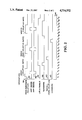
- FIG. 1 is a block diagram of the dual storage device of the present invention employing an NVDRAM, a sense amplifier and a latch;
- FIG. 2 is a timing diagram of the dual storage device of the present invention.
- the input/output, or bit line, of a NVDRAM cell 10 constructed according to the teachings of the related, co-pending application, is shown connected to a first terminal of a bidirectional sense amplifier 12 and, via a transfer transistor 14, to the input terminal to a data latch 16.
- An output terminal of sense amplifier 12 is connected to a first terminal of a second transfer transistor 18 and a second terminal of transistor 18 is connected to an output terminal of data latch 16.
- the NVDRAM cell 10 has a set of control lines which permit selection of the mode of operation of the cell; this selection is described in detail in the related, co-pending application and incorporated herein by reference. Connection of the NVDRAM 10 to the various voltage sources, and the conducting plate and word control lines is not explicitly shown in FIG. 1; these connections being described in detail in the related, co-pending application and incorporated herein by reference.
- the operation and construction of bidirectional sense amplifier 12 and data latch 16 are conventional and well-understood by persons of ordinary skill in the art. Accordingly, they will not be described herein.
- Sense amplifier 12 receives a pair of timing signals, SENSE and SENSE, which, when activated, cause the data at the first terminal of the sense amplifier 12 to be compared to a reference voltage and a signal will subsequently be generated at a second terminal of sense amplifier 12 which corresponds to the complement of the data applied at the first terminal.
- An active timing signal, TRANSFER applied to the gate of transfer transistor 14 causes the signal applied at a first terminal of transistor 14, connected to the sense amplifier 12, to be passed to a second terminal of transistor 14, connected in turn to the input terminal of data latch 16.
- TRANSFER active timing signal applied to the gate of transfer transistor 14 causes a signal applied at the second terminal of transistor 14 to be passed to the first terminal.
- Second transfer transistor 18 also receives the TRANSFER signal at a gate which causes passage of signals between the first and second terminals of transistor 18 in the manner described in connection with transistor 14.
- Data latch 16 receives an ENABLE signal which, when active, causes the latch to retain the data applied to the input terminal until the ENABLE signal is deactivated.
- the signal at the output terminal of data latch 16 follows the signal applied at the input terminal at all times other than when the ENABLE signal is active. Accordingly, a signal generated on the bit line of NVDRAM cell 10 during a READ operation can be applied to the first terminal of the sense amplifier 12 upon application of the SENSE and SENSE signals to sense amplifier 12.
- Application of the TRANSFER signal to transistors 14 and 18, will cause the data read from NVDRAM cell 10 to be transferred from sense amplifier 12 to the data latch 16.
- the NVDRAM cell 10 is responsive to a set of control signals which cause it to perform a variety of operations: a RECALL operation, a STORE operation, a dynamic RAM (DRAM) READ operation, a DRAM WRITE operation, and a REFRESH operation.
- the RECALL operation transfers the data stored within the non-volatile portion of cell 10 to the volatile portion for subsequent generation on the bit line of cell 10. Accordingly, depending on the sequential application of certain of these control signals, the contents of the volatile or the non-volatile portion of NVDRAM cell 10 will be generated at the bit line terminal of cell 10.
- the output terminals of sense amplifier 12 and data latch 16 are connected to a positive input, and a negative input, respectively, of a comparator 20, via signal lines 22 and 24, respectively.
- a COMPARE signal to the comparator 20
- a signal will be generated at an output terminal of comparator 20 indicative of whether the signals at the positive and negative terminals are equal or not.
- these signals at the comparator input terminals will be the contents of the non-volatile and volatile portion, respectively, of the NVDRAM cell 10.
- the circuit illustrated in the block diagram of FIG. 1 can be used to temporarily store and compare the contents of the non-volatile and volatile data stored within a NVDRAM cell.
- FIG. 2 Shown in FIG. 2 are the signals to be applied, in the sequence shown, to the various elements of the circuit illustrated in Fig. 1. While the signals in FIG. 2 are shown active HIGH, the signals may be, in fact, an active LOW, and the following explanation of the circuit elements illustrated in FIG. 1 will nonetheless be equally applicable.
- the control signal applied to the NVDRAM cell 10 which causes a DRAM READ or DRAM WRITE operation to be performed therein is shown in FIG. 2 labelled 50 thereon. As shown, the DRAM READ operation control signal is activated during the time interval beginning at T1 and continuing to T4. In this way, the volatile data is read in the manner described in the related, co-pending application.
- the sense signals applied to the sense amplifier 12, SENSE and SENSE, are shown in FIG. 2 labelled 52 and 54, respectively, and as shown are activated beginning at T2, following T1, and deactivated prior to T4 at T3. In this manner, the volatile data is transferred from the NVDRAM cell to the sense amplifier 12 during the interval T1 to T4.
- an active ENABLE signal 56 is applied to data latch 16 and an active TRANSFER signal 58 is applied to transfer transistors 14 and 18 beginning at T5 and continuing to T6. This causes the volatile data stored within the sense amplifier 12 during the interval T1 to T4, prior to T5, to be transferred to the data latch 16, via transistors 14 and 18, for temporary storage, during the interval ending at T6. Latch ENABLE signal 56 is kept active until at least T13 so that the volatile data will be retained until that time for comparison.
- the RECALL operation control signal 60 is applied to the NVDRAM cell 10, continuing to T8, thereby causing the non-volatile data stored within the cell to be transferred to the volatile portion thereof prior to T8, as described in the related, co-pending application.
- an active DRAM READ operation control signal 50 is applied to NVDRAM cell 10 which causes the non-volatile data to be generated at the bit line of the cell.
- the DRAM READ signal 50 is deactivated at T12, following T9.
- the sense signals SENSE and SENSE, 52 and 54, respectively, are again activated at T10, following T9, and deactivated at T11. In this manner, the non-volatile data is transferred from the NVDRAM cell 10 to the sense amplifier 12 during the interval T9 to T12, as explained above.
- An active COMPARE signal 62 is then applied to the comparator 20 beginning at T13, following T12, and continuing to T14, during which time a signal will be generated at the output of comparator 20 indicative of whether the non-volative and the volatile data accessed from the NVDRAM cell 10 during the intervals T1 to T4 and T7 to T10, respectively, was equal.
- the active ENABLE signal 56 applied to data latch 16 can be deactivated, unless it is needed, as will now be described.
- the circuit illustrated in FIG. 1 can be adapted to perform this replacement as follows: Application of any active TRANSFER signal 58 to transistors 14 and 18 at time T15 will cause the volatile data signal stored within latch 16 to be transferred to the two corresponding terminals of the sense amplifier 12 via transfer transistors 14 and 16, respectively.
- DRAM WRITE operation control signal 50 applied to NVDRAM cell 10 at time T16, following T15, and the subsequent application to sense amplifier 12 of the SENSE and SENSE 52 and 54 signals during the interval T17 to T18, following T16, will cause the volatile data signal to be placed onto signal line 22 and it can be conducted therefrom to the volatile portion of the NVDRAM cell 10 via the bit line in a DRAM WRITE operation, as described more fully in the related, co-pending application.
- DRAM WRITE signal 50, TRANSFER signal 58, and LATCH ENABLE signal 56 are set inactive at times T19, T20 and T21, respectively, following completion of the DRAM WRITE operation at T18.
Abstract
Description
Claims (18)
Priority Applications (1)
| Application Number | Priority Date | Filing Date | Title |
|---|---|---|---|
| US06/717,348 US4716552A (en) | 1985-03-29 | 1985-03-29 | Method and apparatus for non-destructive access of volatile and non-volatile data in a shadow memory array |
Applications Claiming Priority (1)
| Application Number | Priority Date | Filing Date | Title |
|---|---|---|---|
| US06/717,348 US4716552A (en) | 1985-03-29 | 1985-03-29 | Method and apparatus for non-destructive access of volatile and non-volatile data in a shadow memory array |
Publications (1)
| Publication Number | Publication Date |
|---|---|
| US4716552A true US4716552A (en) | 1987-12-29 |
Family
ID=24881659
Family Applications (1)
| Application Number | Title | Priority Date | Filing Date |
|---|---|---|---|
| US06/717,348 Expired - Lifetime US4716552A (en) | 1985-03-29 | 1985-03-29 | Method and apparatus for non-destructive access of volatile and non-volatile data in a shadow memory array |
Country Status (1)
| Country | Link |
|---|---|
| US (1) | US4716552A (en) |
Cited By (18)
| Publication number | Priority date | Publication date | Assignee | Title |
|---|---|---|---|---|
| US5031147A (en) * | 1988-07-26 | 1991-07-09 | Kabushiki Kaisha Toshiba | Semiconductor memory |
| US5136579A (en) * | 1990-10-01 | 1992-08-04 | Rockwell International Corporation | Digital communications network with unlimited channel expandability |
| US5184325A (en) * | 1989-03-10 | 1993-02-02 | Board Of Regents, The University Of Texas System | Dynamic associative memory with logic-in-refresh |
| US5197026A (en) * | 1989-04-13 | 1993-03-23 | Microchip Technology Incorporated | Transparent EEPROM backup of DRAM memories |
| DE4209905C1 (en) * | 1992-03-26 | 1993-05-19 | Siemens Nixdorf Informationssysteme Ag, 4790 Paderborn, De | Memory contents management system using EEPROM and RAM - compares new data with memory image stored in EEPROM, stores changed addresses of locations and writes corresp. contents in EEPROM |
| US5390148A (en) * | 1992-02-25 | 1995-02-14 | Fuji Photo Film Co., Ltd. | Method of rewriting data in EEPROM, and EEPROM card |
| US5680570A (en) * | 1991-06-12 | 1997-10-21 | Quantum Corporation | Memory system with dynamically allocatable non-volatile storage capability |
| US5758148A (en) * | 1989-03-10 | 1998-05-26 | Board Of Regents, The University Of Texas System | System and method for searching a data base using a content-searchable memory |
| US5777608A (en) * | 1989-03-10 | 1998-07-07 | Board Of Regents, The University Of Texas System | Apparatus and method for in-parallel scan-line graphics rendering using content-searchable memories |
| US6097618A (en) * | 1997-12-11 | 2000-08-01 | Cypress Semiconductor Corporation | Apparatus and method for correcting data in a non-volatile random access memory |
| US6148034A (en) * | 1996-12-05 | 2000-11-14 | Linden Technology Limited | Apparatus and method for determining video encoding motion compensation vectors |
| US6249470B1 (en) | 1999-12-03 | 2001-06-19 | International Business Machines Corporation | Bi-directional differential low power sense amp and memory system |
| US20040125644A1 (en) * | 2002-12-31 | 2004-07-01 | Katsuo Komatsuzaki | Multiple bit memory cells and methods for reading non-volatile data |
| US20050083754A1 (en) * | 2002-08-22 | 2005-04-21 | Lovett Simon J. | Method of operating a memory cell |
| US20070140037A1 (en) * | 2005-08-25 | 2007-06-21 | Arun Khamesra | Line driver circuit and method with standby mode of operation |
| US7859906B1 (en) | 2007-03-30 | 2010-12-28 | Cypress Semiconductor Corporation | Circuit and method to increase read margin in non-volatile memories using a differential sensing circuit |
| US7859925B1 (en) | 2006-03-31 | 2010-12-28 | Cypress Semiconductor Corporation | Anti-fuse latch self-test circuit and method |
| WO2015104297A1 (en) * | 2014-01-10 | 2015-07-16 | Commissariat A L'energie Atomique Et Aux Energies Alternatives | Memory provided with associated volatile and non-volatile memory cells |
Citations (2)
| Publication number | Priority date | Publication date | Assignee | Title |
|---|---|---|---|---|
| US3644907A (en) * | 1969-12-31 | 1972-02-22 | Westinghouse Electric Corp | Complementary mosfet memory cell |
| US3798621A (en) * | 1971-12-30 | 1974-03-19 | Ibm | Monolithic storage arrangement with latent bit pattern |
-
1985
- 1985-03-29 US US06/717,348 patent/US4716552A/en not_active Expired - Lifetime
Patent Citations (2)
| Publication number | Priority date | Publication date | Assignee | Title |
|---|---|---|---|---|
| US3644907A (en) * | 1969-12-31 | 1972-02-22 | Westinghouse Electric Corp | Complementary mosfet memory cell |
| US3798621A (en) * | 1971-12-30 | 1974-03-19 | Ibm | Monolithic storage arrangement with latent bit pattern |
Cited By (27)
| Publication number | Priority date | Publication date | Assignee | Title |
|---|---|---|---|---|
| US5031147A (en) * | 1988-07-26 | 1991-07-09 | Kabushiki Kaisha Toshiba | Semiconductor memory |
| US5184325A (en) * | 1989-03-10 | 1993-02-02 | Board Of Regents, The University Of Texas System | Dynamic associative memory with logic-in-refresh |
| US5694406A (en) * | 1989-03-10 | 1997-12-02 | Board Of Regents, The University Of Texas System | Parallel associative processor formed from modified dram |
| US5758148A (en) * | 1989-03-10 | 1998-05-26 | Board Of Regents, The University Of Texas System | System and method for searching a data base using a content-searchable memory |
| US5777608A (en) * | 1989-03-10 | 1998-07-07 | Board Of Regents, The University Of Texas System | Apparatus and method for in-parallel scan-line graphics rendering using content-searchable memories |
| US5197026A (en) * | 1989-04-13 | 1993-03-23 | Microchip Technology Incorporated | Transparent EEPROM backup of DRAM memories |
| US5136579A (en) * | 1990-10-01 | 1992-08-04 | Rockwell International Corporation | Digital communications network with unlimited channel expandability |
| US5680570A (en) * | 1991-06-12 | 1997-10-21 | Quantum Corporation | Memory system with dynamically allocatable non-volatile storage capability |
| US5390148A (en) * | 1992-02-25 | 1995-02-14 | Fuji Photo Film Co., Ltd. | Method of rewriting data in EEPROM, and EEPROM card |
| DE4209905C1 (en) * | 1992-03-26 | 1993-05-19 | Siemens Nixdorf Informationssysteme Ag, 4790 Paderborn, De | Memory contents management system using EEPROM and RAM - compares new data with memory image stored in EEPROM, stores changed addresses of locations and writes corresp. contents in EEPROM |
| US6148034A (en) * | 1996-12-05 | 2000-11-14 | Linden Technology Limited | Apparatus and method for determining video encoding motion compensation vectors |
| US6097618A (en) * | 1997-12-11 | 2000-08-01 | Cypress Semiconductor Corporation | Apparatus and method for correcting data in a non-volatile random access memory |
| US6249470B1 (en) | 1999-12-03 | 2001-06-19 | International Business Machines Corporation | Bi-directional differential low power sense amp and memory system |
| US6363023B2 (en) | 1999-12-03 | 2002-03-26 | International Business Machines Corporation | Bi-directional differential low power sense amp and memory system |
| US7319629B2 (en) | 2002-08-22 | 2008-01-15 | Micron Technology, Inc. | Method of operating a dynamic random access memory cell |
| US20050083754A1 (en) * | 2002-08-22 | 2005-04-21 | Lovett Simon J. | Method of operating a memory cell |
| US20060262612A1 (en) * | 2002-08-22 | 2006-11-23 | Lovett Simon J | Method of operating a memory cell |
| US7206243B2 (en) * | 2002-08-22 | 2007-04-17 | Micron Technology, Inc. | Method of rewriting a logic state of a memory cell |
| US20040125644A1 (en) * | 2002-12-31 | 2004-07-01 | Katsuo Komatsuzaki | Multiple bit memory cells and methods for reading non-volatile data |
| US6944042B2 (en) * | 2002-12-31 | 2005-09-13 | Texas Instruments Incorporated | Multiple bit memory cells and methods for reading non-volatile data |
| US20070140037A1 (en) * | 2005-08-25 | 2007-06-21 | Arun Khamesra | Line driver circuit and method with standby mode of operation |
| US8072834B2 (en) | 2005-08-25 | 2011-12-06 | Cypress Semiconductor Corporation | Line driver circuit and method with standby mode of operation |
| US7859925B1 (en) | 2006-03-31 | 2010-12-28 | Cypress Semiconductor Corporation | Anti-fuse latch self-test circuit and method |
| US7859906B1 (en) | 2007-03-30 | 2010-12-28 | Cypress Semiconductor Corporation | Circuit and method to increase read margin in non-volatile memories using a differential sensing circuit |
| WO2015104297A1 (en) * | 2014-01-10 | 2015-07-16 | Commissariat A L'energie Atomique Et Aux Energies Alternatives | Memory provided with associated volatile and non-volatile memory cells |
| US9620212B2 (en) | 2014-01-10 | 2017-04-11 | Commissariat à l'énergie atomique et aux énergies alternatives | Memory provided with associated volatile and non-volatile memory cells |
| EP3092647B1 (en) * | 2014-01-10 | 2019-04-10 | Commissariat à l'Energie Atomique et aux Energies Alternatives | Memory provided with associated volatile and non-volatile memory cells |
Similar Documents
| Publication | Publication Date | Title |
|---|---|---|
| US4716552A (en) | Method and apparatus for non-destructive access of volatile and non-volatile data in a shadow memory array | |
| US4672580A (en) | Memory cell providing simultaneous non-destructive access to volatile and non-volatile data | |
| US5862099A (en) | Non-volatile programmable memory having a buffering capability and method of operation thereof | |
| US4811294A (en) | Data integrity verifying circuit for electrically erasable and programmable read only memory (EEPROM) | |
| KR950002290B1 (en) | Semiconductor memory device | |
| JP3672954B2 (en) | Semiconductor memory device | |
| US5241503A (en) | Dynamic random access memory with improved page-mode performance and method therefor having isolator between memory cells and sense amplifiers | |
| JP3492168B2 (en) | Nonvolatile semiconductor memory device | |
| US5745403A (en) | System and method for mitigating imprint effect in ferroelectric random access memories utilizing a complementary data path | |
| US6351422B2 (en) | Integrated memory having a differential sense amplifier | |
| US5410505A (en) | Semiconductor memory device having a memory cell unit including a plurality of transistors connected in series | |
| EP0721189B1 (en) | Ferroelectric memory and method for controlling operation of the same | |
| US4069475A (en) | MOS Dynamic random access memory having an improved sense and restore circuit | |
| EP0486550A4 (en) | Single ended sense amplifier with improved data recall from variable bit line current | |
| US5912846A (en) | Serial ferroelectric random access memory architecture to equalize column accesses and improve data retention reliability by mitigating imprint effects | |
| JPH07176184A (en) | Semiconductor memory and writing and reading method for data in the semiconductor memory | |
| US4287576A (en) | Sense amplifying system for memories with small cells | |
| US5081610A (en) | Reference cell for reading eeprom memory devices | |
| US5079745A (en) | Sense amplifier capable of high speed operation | |
| US4134151A (en) | Single sense line memory cell | |
| US5828618A (en) | Line memory | |
| EP0516548A2 (en) | A dynamic random access memory cell | |
| JPS62170097A (en) | Semiconductor storage device | |
| US4004285A (en) | Read-write circuitry for one transistor per bit random access memory | |
| JPH0479098A (en) | Semiconductor storage device |
Legal Events
| Date | Code | Title | Description |
|---|---|---|---|
| AS | Assignment |
Owner name: ADVANCED MICRO DEVICES, INC. 901 THOMPSON PLACE, P Free format text: ASSIGNMENT OF ASSIGNORS INTEREST.;ASSIGNORS:MALTIEL, RON;YAU, ROBERT L.;REEL/FRAME:004392/0925 Effective date: 19850329 |
|
| STCF | Information on status: patent grant |
Free format text: PATENTED CASE |
|
| FEPP | Fee payment procedure |
Free format text: PAYOR NUMBER ASSIGNED (ORIGINAL EVENT CODE: ASPN); ENTITY STATUS OF PATENT OWNER: LARGE ENTITY |
|
| FPAY | Fee payment |
Year of fee payment: 4 |
|
| REFU | Refund |
Free format text: REFUND OF EXCESS PAYMENTS PROCESSED (ORIGINAL EVENT CODE: R169); ENTITY STATUS OF PATENT OWNER: LARGE ENTITY |
|
| FPAY | Fee payment |
Year of fee payment: 8 |
|
| FPAY | Fee payment |
Year of fee payment: 12 |
|
| AS | Assignment |
Owner name: SPANSION INC., CALIFORNIA Free format text: ASSIGNMENT OF ASSIGNORS INTEREST;ASSIGNOR:ADVANCED MICRO DEVICES, INC.;REEL/FRAME:019028/0461 Effective date: 20070131 |
|
| AS | Assignment |
Owner name: SPANSION LLC, CALIFORNIA Free format text: ASSIGNMENT OF ASSIGNORS INTEREST;ASSIGNOR:SPANSION INC.;REEL/FRAME:019063/0765 Effective date: 20070131 |
|
| AS | Assignment |
Owner name: BARCLAYS BANK PLC, NEW YORK Free format text: SECURITY AGREEMENT;ASSIGNORS:SPANSION LLC;SPANSION INC.;SPANSION TECHNOLOGY INC.;AND OTHERS;REEL/FRAME:028840/0001 Effective date: 20100510 |
|
| AS | Assignment |
Owner name: CYPRESS SEMICONDUCTOR CORPORATION, CALIFORNIA Free format text: ASSIGNMENT OF ASSIGNORS INTEREST;ASSIGNOR:SPANSION, LLC;REEL/FRAME:036018/0001 Effective date: 20150601 |