US4777718A - Method of forming and connecting a resistive layer on a pc board - Google Patents
Method of forming and connecting a resistive layer on a pc board Download PDFInfo
- Publication number
- US4777718A US4777718A US06/880,613 US88061386A US4777718A US 4777718 A US4777718 A US 4777718A US 88061386 A US88061386 A US 88061386A US 4777718 A US4777718 A US 4777718A
- Authority
- US
- United States
- Prior art keywords
- substrate
- printed circuit
- resistive
- layer
- circuit board
- Prior art date
- Legal status (The legal status is an assumption and is not a legal conclusion. Google has not performed a legal analysis and makes no representation as to the accuracy of the status listed.)
- Expired - Fee Related
Links
Images

Classifications
-
- H—ELECTRICITY
- H05—ELECTRIC TECHNIQUES NOT OTHERWISE PROVIDED FOR
- H05K—PRINTED CIRCUITS; CASINGS OR CONSTRUCTIONAL DETAILS OF ELECTRIC APPARATUS; MANUFACTURE OF ASSEMBLAGES OF ELECTRICAL COMPONENTS
- H05K1/00—Printed circuits
- H05K1/16—Printed circuits incorporating printed electric components, e.g. printed resistor, capacitor, inductor
- H05K1/167—Printed circuits incorporating printed electric components, e.g. printed resistor, capacitor, inductor incorporating printed resistors
-
- H—ELECTRICITY
- H01—ELECTRIC ELEMENTS
- H01C—RESISTORS
- H01C17/00—Apparatus or processes specially adapted for manufacturing resistors
- H01C17/06—Apparatus or processes specially adapted for manufacturing resistors adapted for coating resistive material on a base
- H01C17/07—Apparatus or processes specially adapted for manufacturing resistors adapted for coating resistive material on a base by resistor foil bonding, e.g. cladding
-
- H—ELECTRICITY
- H01—ELECTRIC ELEMENTS
- H01Q—ANTENNAS, i.e. RADIO AERIALS
- H01Q21/00—Antenna arrays or systems
- H01Q21/0006—Particular feeding systems
- H01Q21/0075—Stripline fed arrays
-
- H—ELECTRICITY
- H05—ELECTRIC TECHNIQUES NOT OTHERWISE PROVIDED FOR
- H05K—PRINTED CIRCUITS; CASINGS OR CONSTRUCTIONAL DETAILS OF ELECTRIC APPARATUS; MANUFACTURE OF ASSEMBLAGES OF ELECTRICAL COMPONENTS
- H05K2201/00—Indexing scheme relating to printed circuits covered by H05K1/00
- H05K2201/03—Conductive materials
- H05K2201/0332—Structure of the conductor
- H05K2201/0335—Layered conductors or foils
- H05K2201/0355—Metal foils
-
- H—ELECTRICITY
- H05—ELECTRIC TECHNIQUES NOT OTHERWISE PROVIDED FOR
- H05K—PRINTED CIRCUITS; CASINGS OR CONSTRUCTIONAL DETAILS OF ELECTRIC APPARATUS; MANUFACTURE OF ASSEMBLAGES OF ELECTRICAL COMPONENTS
- H05K2201/00—Indexing scheme relating to printed circuits covered by H05K1/00
- H05K2201/09—Shape and layout
- H05K2201/09209—Shape and layout details of conductors
- H05K2201/09218—Conductive traces
- H05K2201/09254—Branched layout
-
- H—ELECTRICITY
- H05—ELECTRIC TECHNIQUES NOT OTHERWISE PROVIDED FOR
- H05K—PRINTED CIRCUITS; CASINGS OR CONSTRUCTIONAL DETAILS OF ELECTRIC APPARATUS; MANUFACTURE OF ASSEMBLAGES OF ELECTRICAL COMPONENTS
- H05K2201/00—Indexing scheme relating to printed circuits covered by H05K1/00
- H05K2201/09—Shape and layout
- H05K2201/09209—Shape and layout details of conductors
- H05K2201/095—Conductive through-holes or vias
- H05K2201/09536—Buried plated through-holes, i.e. plated through-holes formed in a core before lamination
-
- H—ELECTRICITY
- H05—ELECTRIC TECHNIQUES NOT OTHERWISE PROVIDED FOR
- H05K—PRINTED CIRCUITS; CASINGS OR CONSTRUCTIONAL DETAILS OF ELECTRIC APPARATUS; MANUFACTURE OF ASSEMBLAGES OF ELECTRICAL COMPONENTS
- H05K2203/00—Indexing scheme relating to apparatus or processes for manufacturing printed circuits covered by H05K3/00
- H05K2203/03—Metal processing
- H05K2203/0361—Stripping a part of an upper metal layer to expose a lower metal layer, e.g. by etching or using a laser
-
- H—ELECTRICITY
- H05—ELECTRIC TECHNIQUES NOT OTHERWISE PROVIDED FOR
- H05K—PRINTED CIRCUITS; CASINGS OR CONSTRUCTIONAL DETAILS OF ELECTRIC APPARATUS; MANUFACTURE OF ASSEMBLAGES OF ELECTRICAL COMPONENTS
- H05K3/00—Apparatus or processes for manufacturing printed circuits
- H05K3/02—Apparatus or processes for manufacturing printed circuits in which the conductive material is applied to the surface of the insulating support and is thereafter removed from such areas of the surface which are not intended for current conducting or shielding
- H05K3/06—Apparatus or processes for manufacturing printed circuits in which the conductive material is applied to the surface of the insulating support and is thereafter removed from such areas of the surface which are not intended for current conducting or shielding the conductive material being removed chemically or electrolytically, e.g. by photo-etch process
-
- H—ELECTRICITY
- H05—ELECTRIC TECHNIQUES NOT OTHERWISE PROVIDED FOR
- H05K—PRINTED CIRCUITS; CASINGS OR CONSTRUCTIONAL DETAILS OF ELECTRIC APPARATUS; MANUFACTURE OF ASSEMBLAGES OF ELECTRICAL COMPONENTS
- H05K3/00—Apparatus or processes for manufacturing printed circuits
- H05K3/40—Forming printed elements for providing electric connections to or between printed circuits
- H05K3/42—Plated through-holes or plated via connections
- H05K3/425—Plated through-holes or plated via connections characterised by the sequence of steps for plating the through-holes or via connections in relation to the conductive pattern
- H05K3/427—Plated through-holes or plated via connections characterised by the sequence of steps for plating the through-holes or via connections in relation to the conductive pattern initial plating of through-holes in metal-clad substrates
-
- H—ELECTRICITY
- H05—ELECTRIC TECHNIQUES NOT OTHERWISE PROVIDED FOR
- H05K—PRINTED CIRCUITS; CASINGS OR CONSTRUCTIONAL DETAILS OF ELECTRIC APPARATUS; MANUFACTURE OF ASSEMBLAGES OF ELECTRICAL COMPONENTS
- H05K3/00—Apparatus or processes for manufacturing printed circuits
- H05K3/46—Manufacturing multilayer circuits
- H05K3/4644—Manufacturing multilayer circuits by building the multilayer layer by layer, i.e. build-up multilayer circuits
- H05K3/4652—Adding a circuit layer by laminating a metal foil or a preformed metal foil pattern
-
- Y—GENERAL TAGGING OF NEW TECHNOLOGICAL DEVELOPMENTS; GENERAL TAGGING OF CROSS-SECTIONAL TECHNOLOGIES SPANNING OVER SEVERAL SECTIONS OF THE IPC; TECHNICAL SUBJECTS COVERED BY FORMER USPC CROSS-REFERENCE ART COLLECTIONS [XRACs] AND DIGESTS
- Y10—TECHNICAL SUBJECTS COVERED BY FORMER USPC
- Y10T—TECHNICAL SUBJECTS COVERED BY FORMER US CLASSIFICATION
- Y10T29/00—Metal working
- Y10T29/49—Method of mechanical manufacture
- Y10T29/49002—Electrical device making
- Y10T29/49082—Resistor making
- Y10T29/49099—Coating resistive material on a base
-
- Y—GENERAL TAGGING OF NEW TECHNOLOGICAL DEVELOPMENTS; GENERAL TAGGING OF CROSS-SECTIONAL TECHNOLOGIES SPANNING OVER SEVERAL SECTIONS OF THE IPC; TECHNICAL SUBJECTS COVERED BY FORMER USPC CROSS-REFERENCE ART COLLECTIONS [XRACs] AND DIGESTS
- Y10—TECHNICAL SUBJECTS COVERED BY FORMER USPC
- Y10T—TECHNICAL SUBJECTS COVERED BY FORMER US CLASSIFICATION
- Y10T29/00—Metal working
- Y10T29/49—Method of mechanical manufacture
- Y10T29/49002—Electrical device making
- Y10T29/49117—Conductor or circuit manufacturing
- Y10T29/49124—On flat or curved insulated base, e.g., printed circuit, etc.
- Y10T29/49126—Assembling bases
-
- Y—GENERAL TAGGING OF NEW TECHNOLOGICAL DEVELOPMENTS; GENERAL TAGGING OF CROSS-SECTIONAL TECHNOLOGIES SPANNING OVER SEVERAL SECTIONS OF THE IPC; TECHNICAL SUBJECTS COVERED BY FORMER USPC CROSS-REFERENCE ART COLLECTIONS [XRACs] AND DIGESTS
- Y10—TECHNICAL SUBJECTS COVERED BY FORMER USPC
- Y10T—TECHNICAL SUBJECTS COVERED BY FORMER US CLASSIFICATION
- Y10T29/00—Metal working
- Y10T29/49—Method of mechanical manufacture
- Y10T29/49002—Electrical device making
- Y10T29/49117—Conductor or circuit manufacturing
- Y10T29/49124—On flat or curved insulated base, e.g., printed circuit, etc.
- Y10T29/49155—Manufacturing circuit on or in base
- Y10T29/49165—Manufacturing circuit on or in base by forming conductive walled aperture in base
Definitions
- This invention relates generally to the transmission of microwave and millimeter-wave energy. Specifically, the present invention relates to an apparatus and method for providing a resistor which is useful in microstrip, stripline, and suspended stripline transmission systems. More specifically, the present invention relates to fabricating a resistor on a printed circuit board using only conventional printed circuit board fabrication techniques.
- a feed network for an antenna may contain hundreds of power dividers or other multiport devices, each of which requires a resistive element.
- Several conventional techniques teach constructing or coupling resistive elements in transmission systems. Although these techniques may work acceptably when only a few resistors are needed, they become impractical in large feed networks which require hundreds of these resistors.
- chip resistors or resistive films may reside at desired locations in the transmission system. These chip resistors or resistive films must be accurately placed and soldered or bonded to a stripline or microstrip printed circuit board to properly connect the resistive element to the transmission system.
- slight displacements, such as 0.005 inch, from an optimum position cause a degraded performance in the transmission system at higher frequencies, such as greater than 10 GHz.
- the probability of degraded performance from a few misplaced resistors becomes great.
- the inductance of solder joints and the effects of adhesives often degrade the performance of the transmission system, and the chip resistors may experience fracturing problems when several layers of printed circuit boards are bonded together to form a multi-layer structure.
- Thick film resistors might also reside at desired locations on a printed circuit board.
- a silk screening operation typically deposits these thick film resistors, and the thick film resistors then cure at elevated temperatures.
- the silk screening technique fails to accurately place the resistive film.
- the elevated temperatures used to cure the resistive film may degrade the adhesion of printed circuit traces to a dielectric substrate.
- the thick film substance, when cured, represents a brittle bump which is subject to cracking when multiple printed circuit boards are bonded together.
- a bi-metallic clad substrate may serve as a printed circuit board on which the microstrip or stripline transmission system is formed.
- Bi-metallic clad substrates have a thin resistive metallic layer clad to a dielectric substrate and a conductive metallic layer clad to the resistive layer.
- a conventional use of a bimetallic clad substrate first removes portions of the conductive metallic layer leaving a desired trace pattern for the feed network. Then, the resistive layer is etched so that resistive material remains clad to the substrate at desired locations. Unfortunately, additional portions of the resistive layer remain sandwiched between the etched conductive metallic traces and the dielectric substrate. This additional portion of the resistive layer causes significant transmission losses at higher frequencies, such as those above 10 GHz.
- Another object of the present invention concerns providing an improved resistive element that is compatible with the lamination of multiple printed circuit boards together into a multi-layer printed circuit board.
- Yet another object of the present invention concerns providing an improved resistive element that minimizes losses at frequencies of greater than 10 GHz.
- Still another object of the present invention concerns providing a resistive element that is suitable for usage on soft printed circuit boards.
- a transmission system which includes two dielectrics that reside substantially parallel to each other.
- Two conductive traces are formed to reside in a plane which contacts a first boundary of one of the dielectrics.
- Each of the two traces have first and second sections.
- a resistive layer resides in contact with a first boundary of the other dielectric.
- the present invention includes means for coupling the resistive layer to the first sections of each of the two conductive traces while preventing the resistive layer from contacting the second sections of each of the two traces.
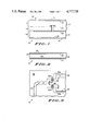
- FIG. 1 shows a cross-sectional side view of a transmission system built according to the teaching of the present invention
- FIG. 2 shows a side view of a middle layer of the transmission system shown in FIG. 1;
- FIG. 3 shows a bottom view of the middle layer shown in FIG. 2;
- FIG. 4 shows a top view of the middle layer shown in FIG. 2;
- FIG. 5 shows a sectional side view of the middle layer shown in FIG. 2 taken after completion of an etching process
- FIG. 6 shows a sectional side view of the transmission system shown in FIG. 1 taken perpendicular to the side view of FIG. 1.
- FIG. 1 shows a transmission system 10 built according to the teaching of the present invention.
- Transmission system 10 contains strata, or layers, 12, 14, and 16.
- Stratum 12 contains a dielectric substrate 18 having a first substantially planar boundary 22 and a second substantially planar boundary 24.
- First boundary 22 resides parallel to second boundary 24 and on an opposing side of dielectric 18 from second boundary 24.
- a conductive layer 30 resides in contact with boundary 22 of stratum 12.
- conductive layer 30 represents a metallic cladding which attaches to substrate 18 at first boundary 22. Copper may advantageously serve as a suitable metal from which conductive layer 30 is constructed.
- Stratum 14 resides adjacent to and substantially parallel with stratum 12.
- Stratum 14 contains conductive traces and at least one resistive element, as discussed below.
- Stratum 16 resides adjacent to and substantially parallel with stratum 14.
- Strata 12 and 16 reside on opposing sides of stratum 14.
- Stratum 16 contains a dielectric substrate 20 which has a first boundary 26 and a second boundary 28.
- First boundary 26 represents a substantially planar surface which resides in contact with stratum 14.
- Second boundary 28 represents a substantially planar surface which resides parallel to boundary 26 and on an opposing side of dielectric 20 from boundary 26.
- a conductive layer 32 resides substantially parallel with and adjacent to dielectric substrate 20 at boundary 28.
- conductive layer 32 represents a metallic cladding, such as copper, attached to dielectric substrate 20.
- transmission system 10 serves as an antenna having a feed network.
- Transmission system 10 represents a multi-layer printed circuit board with strata 12, 14, and 16 representing independent layers which are laminated together.
- Conductive layers 30 and 32 represent top and bottom ground planes for transmission system 10.
- a slot 34 formed in conductive layer 30 permits electromagnetic energy to radiate into and from transmission system 10, causing transmission system 10 to operate as an antenna.
- FIG. 1 illustrates stratum 14 after formation of conductive traces and a resistive element.
- FIG. 2 shows stratum 14 prior to the formation of traces and the resistive element.
- stratum 14 contains a substantially planar dielectric substrate 36 which has a first boundary 38 and a second boundary 40.
- First and second boundaries 38 and 40 reside substantially parallel to each other and on opposing sides of dielectric 36.
- a substantially planar conductive layer 42 resides parallel to and in contact with dielectric 36 at second boundary 40.
- Conductive layer 42 represents a metallic cladding, such as copper, which attaches to dielectric 36.
- a relatively thin resistive metallic layer 44 resides immediately adjacent to dielectric substrate 36 at boundary 38.
- Resistive layer 44 represents a substantially planar surface, advantageously less than 50 micro-inches thick, which adheres at one side thereof to dielectric 36.
- a conductive layer 46 resides substantially parallel with and adjacent to resistive layer 44 on an opposing side of resistive layer 44 from dielectric 36.
- Conductive layer 46 represents a metallic conductor, such as copper, which is conventionally used in fabricating printed circuit boards.
- resistive layer 44 represents a resistive metal which exhibits a predetermined sheet resistivity value, such as 25 or 100 ohms per square. Accordingly, stratum 14 represents a bi-metallic clad substrate.
- Ohmega Foil Clad RT/Duroid manufactured by the Rogers Corporation represents one example of a bimetallic clad substrate.
- the substrate in this preferred embodiment represents a soft substrate.
- transmission system 10 in the preferred embodiment represents a stripline transmission system.
- transmission system 10 in the preferred embodiment represents a stripline transmission system.
- dielectric substrates 18, 20, and 36 need not be constructed from like materials. In fact, air serves as dielectrics 18 and 20 in a suspended stripline application.
- FIGS. 3-5 describe formation of conductive traces and resistive elements on stratum 14 of transmission system 10.
- FIG. 3 shows conductive layer 42 and boundary 40 of stratum 14 after traces have been formed by removing unwanted portions of layer 42.
- the pattern of traces, which conductive layer 42 forms after etching, is constructed by chemical etching using conventional techniques known to those skilled in the art of fabricating printed circuit boards.
- the preferred embodiment shown in FIG. 3 represents a Wilkinson power divider. Accordingly, one common trace splits into two separate traces. The two separate traces are labeled trace 48 and trace 50 in FIG. 3. Traces 48 and 50 provide separate channels which are to be isolated from each other using a resistive element. Trace 48 contains a coupled section 52a and a non-coupled section 54a. Likewise, trace 50 contains a coupled section 52b and a non-coupled section 54b.
- a resistive element connects with traces 48 and 50 at sections 52, and not at sections 54. The location of sections 52 may be determined by one skilled in the art, and sections 54 are defined so that they represent portions of traces 48 and 50 that do not reside within sections 52.
- FIG. 4 shows a view of first boundary 38 of stratum 14.
- FIG. 4 depicts stratum 14 after an etching process has occurred. Two separate etching steps must occur to transform stratum 14 as shown in FIG. 2 into the etched stratum 14 shown in FIG. 4.
- a conventional etching process removes unwanted portions of conductive layer 46. Only pads 60 and 62 from conductive layer 46 remain after this first step. Conductive pads 60 and 62 reside distally from layer 42, directly opposing sections 52a and 52b, respectively (see FIG. 3). In other words, pads 60 and 62 reside in contact with imaginary lines (not shown) that are perpendicular to the plane of traces 48 and 50 and which intersect sections 52a and 52b, respectively.
- the etching of layer 46 may occur simultaneously with the etching of layer 42 (see FIG. 3).
- the chemicals used in etching layer 46 differ from the chemicals used in etching layer 44.
- the etching of layer 46 does not remove a significant portion of resistive layer 44, and the etching of resistive layer 44 does not remove a significant portion of the previously etched layer 46.
- resistive element 68 The portions of resistive layer 46 that remain on boundary 38 of stratum 14 form resistive elements, such as a resistive element 68.
- Resistive element 68 resides on boundary 38 of stratum 14 between pads 60 and 62, on one side of resistive element 68, and boundary 38, on the other side of resistive element 68.
- Resistive element 68 contains a first area 76 which contains first pad 60, and a second area 74, which contains second pad 62.
- pads 60 and 62 couple together only through resistive element 68.
- a particular geometry most advantageously used for resistive element 68 depends upon the impedance of traces 48 and 50 (see FIG. 3) and upon the resistivity of resistive layer 44. Those skilled in the art can design a shape for resistive element 68 so that a predetermined resistance exists between pads 60 and 62.
- conductors 56 and 58 provide electrical paths between pads 60 and 62, respectively, at first ends of conductors 56 and 58 to sections 52a and 52b (see FIG. 3), respectively, at second ends of conductors 56 and 58.
- Pads 60 and 62 contact resistive element 68.
- resistive element 68 electrically couples between separate channels 48 and 50 of the Wilkinson power divider at sections 52a and 52b.
- the present invention exhibits an accuracy in locating resistive element 68 relative to sections 52a and 52b which can be obtained through conventional printed circuit board fabrication techniques. Such an accuracy is typically less than ⁇ 0.003 of an inch even on soft substrates having a relatively large surface area.
- FIG. 5 shows a sectional side view of stratum 14 after conductors 56 and 58 have been installed.
- FIG. 6 shows a sectional side view of transmission system 10 that is taken perpendicular to the FIG. 1 view of transmission system 10.
- conductors 56 and 58 represent plated holes.
- holes are formed through conductive layer 46 at pads 60 and 62, through resistive layer 44 at resistive element 68, through first boundary 38, dielectric substrate 36, second boundary 40, and first conductive layer 42 at traces 48 and 50.
- contact is made with traces 48 and 50 at sections 52, but contact is prevented at sections 54 of traces 48 and 50.
- Hole walls 64 and 66 form as a result.
- Conductive platings 70 and 72 are plated to walls 64 and 66, respectively, using conventional printed circuit board fabrication techniques. Platings 70 and 72 make physical and electrical contact with pads 60 and 62, respectively, and with traces 48 and 50, respectively. Thus, in the preferred embodiment plated holes are used as conductors 56 and 58.
- stratum 14 is bonded, or laminated, with strata 12 and 16 to form a stripline transmission system.
- Conventional multi-layer printed circuit fabrication techniques are used in bonding strata 12, 14, and 16 together. This bonding technique utilizes pressure which may cause the boundaries between strata 12, 14, and 16 to slightly deform away from a perfectly planar surface, but each of these boundaries nevertheless remains substantially planar. Consequently, traces 48 and 50 contact boundary 26 of stratum 16 and resistive element 68 contacts boundary 24 of stratum 12.
- multi-layer printed circuit board technique described in the preferred embodiment which achieves a stripline transmission system may be modified using techniques known to those skilled in the art to cause transmission system 10 to exhibit the properties consistent with a microstrip transmission system, or a suspended stripline transmission system.
Abstract
Description
Claims (1)
Priority Applications (1)
| Application Number | Priority Date | Filing Date | Title |
|---|---|---|---|
| US06/880,613 US4777718A (en) | 1986-06-30 | 1986-06-30 | Method of forming and connecting a resistive layer on a pc board |
Applications Claiming Priority (1)
| Application Number | Priority Date | Filing Date | Title |
|---|---|---|---|
| US06/880,613 US4777718A (en) | 1986-06-30 | 1986-06-30 | Method of forming and connecting a resistive layer on a pc board |
Publications (1)
| Publication Number | Publication Date |
|---|---|
| US4777718A true US4777718A (en) | 1988-10-18 |
Family
ID=25376670
Family Applications (1)
| Application Number | Title | Priority Date | Filing Date |
|---|---|---|---|
| US06/880,613 Expired - Fee Related US4777718A (en) | 1986-06-30 | 1986-06-30 | Method of forming and connecting a resistive layer on a pc board |
Country Status (1)
| Country | Link |
|---|---|
| US (1) | US4777718A (en) |
Cited By (27)
| Publication number | Priority date | Publication date | Assignee | Title |
|---|---|---|---|---|
| US4831345A (en) * | 1988-06-17 | 1989-05-16 | The United States Of America As Represented By The Secretary Of The Navy | Stripline power divider |
| US5216404A (en) * | 1990-07-25 | 1993-06-01 | Matsushita Electric Industrial Co., Ltd. | Sic thin-film thermistor |
| US5347258A (en) * | 1993-04-07 | 1994-09-13 | Zycon Corporation | Annular resistor coupled with printed circuit board through-hole |
| US5521357A (en) * | 1992-11-17 | 1996-05-28 | Heaters Engineering, Inc. | Heating device for a volatile material with resistive film formed on a substrate and overmolded body |
| EP0795908A2 (en) * | 1996-03-14 | 1997-09-17 | Dassault Electronique | Multilayer high frequency circuit with integrated active elements |
| US5831510A (en) * | 1994-05-16 | 1998-11-03 | Zhang; Michael | PTC electrical devices for installation on printed circuit boards |
| US5852397A (en) * | 1992-07-09 | 1998-12-22 | Raychem Corporation | Electrical devices |
| US5994997A (en) * | 1997-11-24 | 1999-11-30 | Motorola, Inc. | Thick-film resistor having concentric terminals and method therefor |
| US6108212A (en) * | 1998-06-05 | 2000-08-22 | Motorola, Inc. | Surface-mount device package having an integral passive component |
| US6281090B1 (en) * | 1996-10-16 | 2001-08-28 | Macdermid, Incorporated | Method for the manufacture of printed circuit boards with plated resistors |
| US20020162214A1 (en) * | 1999-09-14 | 2002-11-07 | Scott Hetherton | Electrical devices and process for making such devices |
| US6640420B1 (en) | 1999-09-14 | 2003-11-04 | Tyco Electronics Corporation | Process for manufacturing a composite polymeric circuit protection device |
| US6794956B2 (en) * | 2001-09-12 | 2004-09-21 | Murata Manufacturing Co., Ltd. | Circuit substrate having resistive films connecting external terminals in series with lands |
| US20050139391A1 (en) * | 2002-06-12 | 2005-06-30 | Intel Corporation | Circuit board with trace configuration for high-speed digital differential signaling |
| US20060286696A1 (en) * | 2005-06-21 | 2006-12-21 | Peiffer Joel S | Passive electrical article |
| US20070222551A1 (en) * | 2006-03-21 | 2007-09-27 | Ying-Jiunn Lai | Film resistor embedded in multi-layer circuit board and manufacturing method thereof |
| US20090002092A1 (en) * | 2005-11-30 | 2009-01-01 | Selex Sensors And Airborne Systems Limited | Microwave Power Splitter/Combiner |
| US20090241333A1 (en) * | 2008-03-28 | 2009-10-01 | Fukui Precision Component (Shenzhen) Co., Ltd. | Method for manufacturing printed circuit board having different thicknesses in different areas |
| US7626828B1 (en) * | 2003-07-30 | 2009-12-01 | Teradata Us, Inc. | Providing a resistive element between reference plane layers in a circuit board |
| US20100032830A1 (en) * | 2008-08-06 | 2010-02-11 | Industrial Technology Research Institute | Three-dimensional conducting structure and method of fabricating the same |
| US20110032049A1 (en) * | 2008-04-11 | 2011-02-10 | Mitsubishi Electric Corporation | Power divider |
| US20120098635A1 (en) * | 2010-10-26 | 2012-04-26 | Renesas Electronics Corporation | Resistive element and manufacturing method therefor |
| TWI387087B (en) * | 2008-08-06 | 2013-02-21 | Ind Tech Res Inst | Three-dimensional conducting structure and method of fabricating the same |
| US9078371B2 (en) | 2012-10-15 | 2015-07-07 | Raytheon Company | Radiofrequency absorptive filter |
| DE102014015516A1 (en) | 2014-10-20 | 2016-04-21 | Protemics GmbH | Absorber microstructure for attenuation of microwave and terahertz signals on strip lines and planar waveguides |
| EP4075597A1 (en) * | 2013-10-29 | 2022-10-19 | Zoll Medical Israel Ltd. | Antenna systems and devices and methods of manufacture thereof |
| US11872012B2 (en) | 2017-08-10 | 2024-01-16 | Zoll Medical Israel Ltd. | Systems, devices and methods for physiological monitoring of patients |
Citations (13)
| Publication number | Priority date | Publication date | Assignee | Title |
|---|---|---|---|---|
| US3354412A (en) * | 1965-11-01 | 1967-11-21 | Emc Technology Inc | Stripline termination device having a resistor that is shorter than one quarter wavelength |
| US3423260A (en) * | 1966-03-21 | 1969-01-21 | Bunker Ramo | Method of making a thin film circuit having a resistor-conductor pattern |
| US3541474A (en) * | 1969-07-31 | 1970-11-17 | Bell Telephone Labor Inc | Microwave transmission line termination |
| US3585533A (en) * | 1970-02-26 | 1971-06-15 | Sperry Rand Corp | Microwave microcircuit element with resistive high grequency energy absorber |
| US3678417A (en) * | 1971-07-14 | 1972-07-18 | Collins Radio Co | Planar r. f. load resistor for microstrip or stripline |
| US3771070A (en) * | 1972-12-22 | 1973-11-06 | Us Air Force | Stripline-to-two-conductor balun |
| US3775725A (en) * | 1970-04-30 | 1973-11-27 | Hokuriku Elect Ind | Printed resistor |
| US3815055A (en) * | 1973-04-20 | 1974-06-04 | Raytheon Co | Microwave power divider |
| US3974462A (en) * | 1972-03-07 | 1976-08-10 | Raytheon Company | Stripline load for airborne antenna system |
| US4189691A (en) * | 1977-11-11 | 1980-02-19 | Raytheon Company | Microwave terminating structure |
| US4396900A (en) * | 1982-03-08 | 1983-08-02 | The United States Of America As Represented By The Secretary Of The Navy | Thin film microstrip circuits |
| US4450418A (en) * | 1981-12-28 | 1984-05-22 | Hughes Aircraft Company | Stripline-type power divider/combiner with integral resistor and method of making the same |
| EP0148506A2 (en) * | 1983-12-26 | 1985-07-17 | Hitachi, Ltd. | Circuit board |
-
1986
- 1986-06-30 US US06/880,613 patent/US4777718A/en not_active Expired - Fee Related
Patent Citations (13)
| Publication number | Priority date | Publication date | Assignee | Title |
|---|---|---|---|---|
| US3354412A (en) * | 1965-11-01 | 1967-11-21 | Emc Technology Inc | Stripline termination device having a resistor that is shorter than one quarter wavelength |
| US3423260A (en) * | 1966-03-21 | 1969-01-21 | Bunker Ramo | Method of making a thin film circuit having a resistor-conductor pattern |
| US3541474A (en) * | 1969-07-31 | 1970-11-17 | Bell Telephone Labor Inc | Microwave transmission line termination |
| US3585533A (en) * | 1970-02-26 | 1971-06-15 | Sperry Rand Corp | Microwave microcircuit element with resistive high grequency energy absorber |
| US3775725A (en) * | 1970-04-30 | 1973-11-27 | Hokuriku Elect Ind | Printed resistor |
| US3678417A (en) * | 1971-07-14 | 1972-07-18 | Collins Radio Co | Planar r. f. load resistor for microstrip or stripline |
| US3974462A (en) * | 1972-03-07 | 1976-08-10 | Raytheon Company | Stripline load for airborne antenna system |
| US3771070A (en) * | 1972-12-22 | 1973-11-06 | Us Air Force | Stripline-to-two-conductor balun |
| US3815055A (en) * | 1973-04-20 | 1974-06-04 | Raytheon Co | Microwave power divider |
| US4189691A (en) * | 1977-11-11 | 1980-02-19 | Raytheon Company | Microwave terminating structure |
| US4450418A (en) * | 1981-12-28 | 1984-05-22 | Hughes Aircraft Company | Stripline-type power divider/combiner with integral resistor and method of making the same |
| US4396900A (en) * | 1982-03-08 | 1983-08-02 | The United States Of America As Represented By The Secretary Of The Navy | Thin film microstrip circuits |
| EP0148506A2 (en) * | 1983-12-26 | 1985-07-17 | Hitachi, Ltd. | Circuit board |
Non-Patent Citations (2)
| Title |
|---|
| Trant, G. R.; "Microwave Stripline Packaging with UMD's"; Microwave Journal; Aug. 1975; pp. 49-51. |
| Trant, G. R.; Microwave Stripline Packaging with UMD s ; Microwave Journal; Aug. 1975; pp. 49 51. * |
Cited By (48)
| Publication number | Priority date | Publication date | Assignee | Title |
|---|---|---|---|---|
| US4831345A (en) * | 1988-06-17 | 1989-05-16 | The United States Of America As Represented By The Secretary Of The Navy | Stripline power divider |
| US5216404A (en) * | 1990-07-25 | 1993-06-01 | Matsushita Electric Industrial Co., Ltd. | Sic thin-film thermistor |
| US6651315B1 (en) | 1992-07-09 | 2003-11-25 | Tyco Electronics Corporation | Electrical devices |
| US5852397A (en) * | 1992-07-09 | 1998-12-22 | Raychem Corporation | Electrical devices |
| US20040246092A1 (en) * | 1992-07-09 | 2004-12-09 | Graves Gregory A. | Electrical devices |
| US7355504B2 (en) | 1992-07-09 | 2008-04-08 | Tyco Electronics Corporation | Electrical devices |
| US5521357A (en) * | 1992-11-17 | 1996-05-28 | Heaters Engineering, Inc. | Heating device for a volatile material with resistive film formed on a substrate and overmolded body |
| US5347258A (en) * | 1993-04-07 | 1994-09-13 | Zycon Corporation | Annular resistor coupled with printed circuit board through-hole |
| US6292088B1 (en) | 1994-05-16 | 2001-09-18 | Tyco Electronics Corporation | PTC electrical devices for installation on printed circuit boards |
| US5831510A (en) * | 1994-05-16 | 1998-11-03 | Zhang; Michael | PTC electrical devices for installation on printed circuit boards |
| EP0795908A2 (en) * | 1996-03-14 | 1997-09-17 | Dassault Electronique | Multilayer high frequency circuit with integrated active elements |
| EP0795908A3 (en) * | 1996-03-14 | 1999-09-29 | Dassault Electronique | Multilayer high frequency circuit with integrated active elements |
| US6281090B1 (en) * | 1996-10-16 | 2001-08-28 | Macdermid, Incorporated | Method for the manufacture of printed circuit boards with plated resistors |
| US6130601A (en) * | 1997-11-24 | 2000-10-10 | Motorola, Inc. | Thick-film resistor having concentric terminals and method therefor |
| US5994997A (en) * | 1997-11-24 | 1999-11-30 | Motorola, Inc. | Thick-film resistor having concentric terminals and method therefor |
| US6108212A (en) * | 1998-06-05 | 2000-08-22 | Motorola, Inc. | Surface-mount device package having an integral passive component |
| US20020162214A1 (en) * | 1999-09-14 | 2002-11-07 | Scott Hetherton | Electrical devices and process for making such devices |
| US20040090304A1 (en) * | 1999-09-14 | 2004-05-13 | Scott Hetherton | Electrical devices and process for making such devices |
| US6640420B1 (en) | 1999-09-14 | 2003-11-04 | Tyco Electronics Corporation | Process for manufacturing a composite polymeric circuit protection device |
| US6854176B2 (en) | 1999-09-14 | 2005-02-15 | Tyco Electronics Corporation | Process for manufacturing a composite polymeric circuit protection device |
| US7343671B2 (en) | 1999-09-14 | 2008-03-18 | Tyco Electronics Corporation | Process for manufacturing a composite polymeric circuit protection device |
| WO2002001636A1 (en) * | 2000-06-27 | 2002-01-03 | Macdermid, Incorporated | Process for the manufacture of printed circuit boards with plated resistors |
| US6794956B2 (en) * | 2001-09-12 | 2004-09-21 | Murata Manufacturing Co., Ltd. | Circuit substrate having resistive films connecting external terminals in series with lands |
| US20050139391A1 (en) * | 2002-06-12 | 2005-06-30 | Intel Corporation | Circuit board with trace configuration for high-speed digital differential signaling |
| US20060261465A1 (en) * | 2002-06-12 | 2006-11-23 | Intel Corporation | Circuit board with trace configuration for high-speed digital differential signaling |
| US7145239B2 (en) * | 2002-06-12 | 2006-12-05 | Intel Corporation | Circuit board with trace configuration for high-speed digital differential signaling |
| US7417872B2 (en) * | 2002-06-12 | 2008-08-26 | Intel Corporation | Circuit board with trace configuration for high-speed digital differential signaling |
| US7626828B1 (en) * | 2003-07-30 | 2009-12-01 | Teradata Us, Inc. | Providing a resistive element between reference plane layers in a circuit board |
| US20060286696A1 (en) * | 2005-06-21 | 2006-12-21 | Peiffer Joel S | Passive electrical article |
| US20100208440A1 (en) * | 2005-06-21 | 2010-08-19 | 3M Innovative Properties Company | Passive electrical article |
| US20090002092A1 (en) * | 2005-11-30 | 2009-01-01 | Selex Sensors And Airborne Systems Limited | Microwave Power Splitter/Combiner |
| US7920035B2 (en) | 2005-11-30 | 2011-04-05 | Selex Galileo Ltd. | Microwave power splitter/combiner |
| US7830241B2 (en) * | 2006-03-21 | 2010-11-09 | Industrial Technology Research Institute | Film resistor embedded in multi-layer circuit board and manufacturing method thereof |
| US20070222551A1 (en) * | 2006-03-21 | 2007-09-27 | Ying-Jiunn Lai | Film resistor embedded in multi-layer circuit board and manufacturing method thereof |
| US7987586B2 (en) * | 2008-03-28 | 2011-08-02 | Fukui Precision Component (Shenzhen) Co., Ltd. | Method for manufacturing printed circuit board having different thicknesses in different areas |
| US20090241333A1 (en) * | 2008-03-28 | 2009-10-01 | Fukui Precision Component (Shenzhen) Co., Ltd. | Method for manufacturing printed circuit board having different thicknesses in different areas |
| US20110032049A1 (en) * | 2008-04-11 | 2011-02-10 | Mitsubishi Electric Corporation | Power divider |
| US8471647B2 (en) * | 2008-04-11 | 2013-06-25 | Mitsubishi Electric Corporation | Power divider |
| TWI387087B (en) * | 2008-08-06 | 2013-02-21 | Ind Tech Res Inst | Three-dimensional conducting structure and method of fabricating the same |
| US20100032830A1 (en) * | 2008-08-06 | 2010-02-11 | Industrial Technology Research Institute | Three-dimensional conducting structure and method of fabricating the same |
| US8193632B2 (en) * | 2008-08-06 | 2012-06-05 | Industrial Technology Research Institute | Three-dimensional conducting structure and method of fabricating the same |
| US20120098635A1 (en) * | 2010-10-26 | 2012-04-26 | Renesas Electronics Corporation | Resistive element and manufacturing method therefor |
| US8289126B2 (en) * | 2010-10-26 | 2012-10-16 | Renesas Electronics Corporation | Resistive element and manufacturing method therefor |
| US9078371B2 (en) | 2012-10-15 | 2015-07-07 | Raytheon Company | Radiofrequency absorptive filter |
| EP4075597A1 (en) * | 2013-10-29 | 2022-10-19 | Zoll Medical Israel Ltd. | Antenna systems and devices and methods of manufacture thereof |
| US11539125B2 (en) | 2013-10-29 | 2022-12-27 | Zoll Medical Israel Ltd. | Antenna systems and devices, and methods of manufacture thereof |
| DE102014015516A1 (en) | 2014-10-20 | 2016-04-21 | Protemics GmbH | Absorber microstructure for attenuation of microwave and terahertz signals on strip lines and planar waveguides |
| US11872012B2 (en) | 2017-08-10 | 2024-01-16 | Zoll Medical Israel Ltd. | Systems, devices and methods for physiological monitoring of patients |
Similar Documents
| Publication | Publication Date | Title |
|---|---|---|
| US4777718A (en) | Method of forming and connecting a resistive layer on a pc board | |
| EP0439928B1 (en) | Directional stripline structure and manufacture | |
| US5311406A (en) | Microstrip printed wiring board and a method for making same | |
| US3501831A (en) | Eyelet | |
| US6777622B2 (en) | Wiring boards | |
| EP0469308B1 (en) | Multilayered circuit board assembly and method of making same | |
| US4329779A (en) | Methods of applying circuit elements to a substrate | |
| US6765455B1 (en) | Multi-layered spiral couplers on a fluropolymer composite substrate | |
| EP0343400A2 (en) | Electronic package assembly with flexible carrier and method of making it | |
| TW202017451A (en) | Method of manufacturing circuit board | |
| US8076591B2 (en) | Circuit boards | |
| KR100489820B1 (en) | Ceramic Multilayer Substrate and its Manufacturing Process | |
| US20040150487A1 (en) | Semi-suspended coplanar waveguide on a printed circuit board | |
| US4737747A (en) | Printed circuit resistive element | |
| US6917265B2 (en) | Microwave frequency surface mount components and methods of forming same | |
| CN110876226A (en) | Rigid-flexible circuit board and manufacturing method thereof | |
| JP3347607B2 (en) | Laminated waveguide line | |
| JPH05327211A (en) | Multilayer flexible printed board and manufacture thereof | |
| US4916808A (en) | Process for fabricating a sculptured stripling interface conductor | |
| JP2015185550A (en) | Multilayer high-frequency substrate, and antenna device | |
| KR20010093792A (en) | Microwave mixer with baluns having rectangular coaxial transmission line | |
| EP1187514A2 (en) | Printed wiring board | |
| US5763060A (en) | Printed wiring board | |
| JP2000068716A (en) | Multilayer transmission line | |
| KR930002515B1 (en) | Tab tape for high frequency semiconductor device |
Legal Events
| Date | Code | Title | Description |
|---|---|---|---|
| AS | Assignment |
Owner name: MOTOROLA, INC., SCHAUMBURG, ILLINOIS, A CORP. OF D Free format text: ASSIGNMENT OF ASSIGNORS INTEREST.;ASSIGNORS:HENDERSON, JAMES M.;KIELMEYER, RONALD F. JR.;REEL/FRAME:004574/0880 Effective date: 19860624 |
|
| FEPP | Fee payment procedure |
Free format text: PAYOR NUMBER ASSIGNED (ORIGINAL EVENT CODE: ASPN); ENTITY STATUS OF PATENT OWNER: LARGE ENTITY |
|
| FPAY | Fee payment |
Year of fee payment: 4 |
|
| REMI | Maintenance fee reminder mailed | ||
| LAPS | Lapse for failure to pay maintenance fees | ||
| FP | Lapsed due to failure to pay maintenance fee |
Effective date: 19961023 |
|
| STCH | Information on status: patent discontinuation |
Free format text: PATENT EXPIRED DUE TO NONPAYMENT OF MAINTENANCE FEES UNDER 37 CFR 1.362 |