US4797179A - Fabrication of integral lenses on LED devices - Google Patents
Fabrication of integral lenses on LED devices Download PDFInfo
- Publication number
- US4797179A US4797179A US07/060,772 US6077287A US4797179A US 4797179 A US4797179 A US 4797179A US 6077287 A US6077287 A US 6077287A US 4797179 A US4797179 A US 4797179A
- Authority
- US
- United States
- Prior art keywords
- wafer
- mesas
- etching
- chemical etchant
- bpk
- Prior art date
- Legal status (The legal status is an assumption and is not a legal conclusion. Google has not performed a legal analysis and makes no representation as to the accuracy of the status listed.)
- Expired - Lifetime
Links
Images


Classifications
-
- H—ELECTRICITY
- H01—ELECTRIC ELEMENTS
- H01L—SEMICONDUCTOR DEVICES NOT COVERED BY CLASS H10
- H01L33/00—Semiconductor devices with at least one potential-jump barrier or surface barrier specially adapted for light emission; Processes or apparatus specially adapted for the manufacture or treatment thereof or of parts thereof; Details thereof
- H01L33/02—Semiconductor devices with at least one potential-jump barrier or surface barrier specially adapted for light emission; Processes or apparatus specially adapted for the manufacture or treatment thereof or of parts thereof; Details thereof characterised by the semiconductor bodies
- H01L33/20—Semiconductor devices with at least one potential-jump barrier or surface barrier specially adapted for light emission; Processes or apparatus specially adapted for the manufacture or treatment thereof or of parts thereof; Details thereof characterised by the semiconductor bodies with a particular shape, e.g. curved or truncated substrate
Definitions
- the invention relates to the fabrication of integral lenses on LED devices, and particularly to the fabrication of spherical lenses having both good quality and high yields for the commercial fabrication of large quantities.
- a light-emitting diode is a pn junction semiconductor device designed to emit light when forward biased.
- the light can be one of several visible colors such as red, amber, yellow, or green, or it can be infrared and thus invisible.
- an LED is similar to a conventional diode in that it has a relatively low forward voltage threshold. Once this threshold is exceeded, the junction has a low impedance and conducts current readily. This current is limited by an external circuit, usually a resistor.
- the amount of light emitted by an LED is typically proportional to the forward current over a broad range; thus, it is relatively easily controlled, either linearly or by pulsing.
- LED devices are used in a wide variety of commercial systems and many of these systems have the LED devices coupling radiation into optical fibers. It is known in the prior art such as from the article entitled, "Coupling of Spherical-Surfaced LED and Spherical-Ended Fiber" by Osamu Hasegawa, Ryosuke Namazu, Masayuki Abe and Yoshikazu Toyama, J. Appl. Phys. Vol. 51 (1), January 1980, pp. 30-36 that the launching efficiency for radiation from an LED device having a spherical lens is generally superior to that using an LED device with no lens. This article does not disclose information relating to the fabrication of spherical lenses.
- Integrated spherical lenses for LED devices have also been analyzed and studied experimentally. Reported data confirm that LED devices having spherical lenses are much better than flat LED devices for specific types of LED devices such as laser diodes and infrared light emitting diodes according to the article entitled "High-Radiance Surface-Emitting (In,Ga) (As,P)/InP IREDS" by J. Heinen and Ch. Lauterbach, Siemens Forsch.-8 Entwick-lungsber, 1982, Vol. 11.
- This article discloses general steps of fabricating a spherical lens on an LED device by first chemically etching a mesa extending above a wafer surface and thereafter, chemically etching the mesa to round out the edges and the top of the mesa to form a spherical lens.
- the article does not include any specific details for fabricating the lenses.
- Heinen discloses fabricating a lens by first chemically etching a circular mesa in the substrate centered to the emitting area. A conventional masking of a circular masked area was used. Heinen used bromine:methanol (1:40) as the chemical etchant. The etch mask used to form the mesa was removed and the same etchant was used on the mesa to round it into a spherical lens. The spherical lens extended above the surface of the LED device.
- an integrated spherical lens is preferably well formed to focus radiation optimally. Deviations from a true spherical lens can produce losses in the transfer of radiation from an LED device to an optical fiber or other components in an optical system.
- a well shaped spherical lens can be etched from a well shaped mesa using an isotropic chemical etchant.
- a well shaped mesa has circular cross sections which are concentric and also has a top generally parallel to the surface of the LED device.
- an "isotropic chemical etchant" as used herein etches a flat surface of a specific material equally in all directions.
- mesas having circular cross sections can be achieved with an isotropic chemical etchant for the wafers used to fabricate the LED devices.
- the lenses are fabricated in the portion of the wafer composed of InP.
- the mesas extend above the surface of the wafer in each case.
- Some chemical etchants suitable for etching InP are disclosed in the article entitled, "Chemical Etching Characteristics of (001) InP", by Sadao Adachi and Hitoshi Kawaguchi, J. Electrochem. Soc., June 1981, pp. 1342-1349. These chemical etchants include (1) HCl systems, (2) HCl:HNO 3 systems, (3) HBr systems, (4) H 2 SO 4 :H 2 O 2 :H 2 O systems, and Br 2 :CH 3 OH system. The article discloses the capabilities of these etchants to etch isotropically for applications such as etching mesas extending above the surface of a wafer.
- Adachi discloses that the etching rate of BPK is greater for a stirred solution than a non-stirred solution. Stirring does not produce a sufficiently random movement of the BPK to avoid non-uniform etching. Non-stirred solutions are preferable for etching. Adachi shows that a non-stirred BPK solution can etch a relatively pit free surface for concentrations greater than a certain level. Furthermore, for relatively low concentrations, the BPK solution tends to produce pits. Adachi concludes that the BPK is a good isotropic chemical etchant for both InP and InGaAsP/InP double heterostructure wafers and can be used to produce mesa-shaped structures with good resist pattern definition. Adachi does not, however, consider the suitability of the BPK for fabricating an integrated lens on an LED device.
- An integral lens on an LED device can also be fabricated using photoelectrochemical etching as disclosed in the article entitled, "Photoelectrochemical Etching of Integral Lenses on InGaAsP/InP Light-Emitting Diodes", by F. W. Ostermayer, Jr., P. A. Kohl and R. H. Burton, Appl. Phys. Lett., Vol. 43, No. 7, October 1983, pp. 642-644.
- the invention disclosed herein relates to the use of a chemical etchant.
- the article is of interest because it discloses etched lenses which are below the surface of the LED device. There is no disclosure in the article relative to the advantages of such a configuration.
- the commercial fabrication of LED devices is typically carried out using a wafer as large as about 2 cm. by 2 cm. with a plurality of LED devices being formed in the wafer.
- Some of the difficulties in fabricating integrated lenses include chemically etching uniform mesas heights across the wafer and thereafter, etching smooth, well-defined spherical lenses from the mesas.
- the mesas are produced by chemically etching the wafer surface around etch masks defining the top surfaces of the mesas. The etch masks are removed, and thereafter, the mesas are etched into spherical lenses.
- spherical lenses extend above the surface of a wafer and can be damaged relatively easily during subsequent processing steps. It has now been concluded that damages to lenses can be minimized by fabricating integrated spherical lenses below the surface of the wafer. Furthermore, the spherical lenses can be fabricated so that much less of the surface of the wafer is etched as compared to the prior art process.
- the invention relates to fabricating integrated spherical lenses on LED devices.
- An isotropic chemical etchant such as BPK is used on a wafer having a plurality of InGaAsP/InP light emitting diodes (LED).
- a conventional etchant mask is used to etch mesas.
- the etchant mask defines solid circular first portions over the regions of the LED's on the wafer from which radiations are to be emitted and a solid second portion spaced away from the first portions to define unmasked areas of the wafer around each first portion.
- the unmasked areas between the first and second portions are not annular openings. These unmasked areas are selected so that chemical etching produces mesas having substantially circular cross sections.
- the second portion defines square openings oriented so that the diagonals substantially start at the (111A) planes and each square opening has its center substantially at the center of the associated first portion.
- the BPK is suitable for the chemical etchant.
- the etchant mask is removed using commercial methods and the mesas are chemically etched to produce spherical lenses.
- the BPK is also suitable for this etching. This etching can be carried out using conventional techniques.
- the spherical lenses fabricated according to the invention are recessed below the surface of the wafer and are well shaped over most of the wafer.
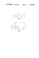
- FIG. 1 is a plan view of a wafer masked for chemically etching mesas according to the prior art
- FIG. 2 is a typical cross sectional view of some mesas produced by chemically etching the masked wafer shown in FIG. 1;
- FIG. 3 is a plan view of a wafer masked for chemically etching mesas for fabricating recessed spherical lenses according to the prior art
- FIG. 4 is a cross sectional view on an enlarged scale of some mesas obtained by chemically etching the masked wafer shown in FIG. 3;
- FIG. 5 shows a plan view of a wafer masked for etching mesas in accordance with the invention.
- FIG. 6 is a graph relating spherical lens radius to chemical etch time for a mesa using BPK.
- FIG. 1 shows a typical prior art masking arrangement for chemically etching mesas for fabricating integral spherical lenses on LED devices.
- a wafer 10 has circular masks 12 positioned above the areas from which radiation is emitted by each of the LED devices defined in the wafer 10.
- the masks are fabricated using conventional techniques and can be made of SiO 2 or a photoresist if a compatible chemical etchant is used. Thereafter, the wafer is isotropically chemically etched in a conventional method to produce a plurality of mesas corresponding to each of the masks 12.
- FIG. 2 shows a typical cross sectional view for some mesas 14 produced from etching the wafer 10.
- the mesas 14 produced near the edges of the wafer 10 are not as well defined as the mesas 14 produced in the central area of the wafer 10.
- the mesas 14 near the edges have deeper undercuts than the centrally located mesas 14 and the deeper undercut mesas 14 produce spherical lenses with small radii. Lenses with large radii are generally more desirable for many applications.
- the mesas 14 near the edges result in unusable LED devices, thereby reducing the yield for the fabrication process.
- etching the mesas 14 Another problem in etching the mesas 14 is that the heights of the mesas 14 above the surface of the wafer can vary from the mesas 14 at the edges of the wafer 10 to the mesas 14 at the central portion of the wafer 10. This is particularly evident for relatively large wafers.
- the etchant is maintained stagnant during the etching because stirring usually produces non-uniform etching patterns.
- the stagnant etching is a diffusion-controlled process.
- the edges of the wafer 10 have a greater opportunity for etchant replenishment than the central portion of the wafer 10 so that the edges can be etched faster. Maintaining the wafer level in the chemical etchant tends to reduce this problem by minimizing an apparent flow of the etchant over the surface of the wafer.
- the next conventional processing step for the wafer 10 is the removal of the masks 12 from the mesas 14. Subsequently, the mesas 14 are chemically etched to transform the upper portions of the mesas 14 from being flat to being spherical. Accordingly, integral lenses on the LED devices are produced and these spherical lenses are raised above the surface 16 of the wafer 10. It has been found that during additional production operations, the raised spherical lenses can be damaged. Such damage includes lenses being broken off, or being scratched, or being otherwise deformed.
- Recessed spherical lenses were produced by the use of a masked arrangement as shown in FIG. 3.
- a wafer 30 having a plurality of LED devices defined therein has circular masking portions 32 positioned over the areas from which radiation will be emitted from each LED device.
- circular masking portion 34 defining annular openings 36 around the masking portions 32 is on the wafer 30.
- the wafer 30 corresponds to the wafer 10 so that the spacing between emitting areas of the respective LED devices are the same.
- the spacing between circular masking portions 32 is substantially the same as the spacing between the circular masking portions 12. This implies a limitation on the maximum radius of the annular openings 36 in order to provide space on each LED device for ball bonding.
- FIG. 4 shows a portion of a cross sectional view of a wafer 40, having some mesas having sides 42 which are relatively flat rather than curved. The flat sides 42 are believed to be due to the (111) plane.
- an isotropic chemical etchant such as BPK etches substantially isotropically but in this situation it etches anisotropically. It is believed that a relatively small annular opening for the chemical etching does not provide a good opportunity for the etchant to etch other planes around the (111A) planes.
- a test was conducted, using relatively large annular openings and it was found that mesas having relatively good circular cross sections were obtained. This method requires a larger area for each LED device relative to the area used in FIG. 1 because of the space needed on each device for ball bonding. This method of overcoming the problem is economically unattractive because it reduces the number of LED devices which can be produced for each wafer.
- the wafer 50 has a plurality of LED devices defined in it.
- the mask can be Si:O 2 or a photoresist, or the like.
- the mask is selected to be resistive to attack or deterioration due to the chemical etchant.
- the mask is applied and formed into the masking arrangement using conventional techniques.
- Each circular masking portion 52 covers the area from which radiation will be emitted from an LED device and a second masking portion 54 defines square openings 56.
- the spacing between the circular masking portion 52 can correspond to the spacing between the circular masking portion 12 in FIG. 1.
- each square opening 56 is oriented 45 degrees relative to the cleaved wafer edges that surround the respective mesa to be etched.
- the square openings 56 in FIG. 5 have the (111A) planes at the diagonals while the edges of the square openings 56 provide sufficient room for each LED device for ball bonding.
- the masking arrangement shown in FIG. 5 compensates for the different etching rates in different directions of an isotropic chemical etchant which etches anisotropically for a relatively small mask opening.
- the chemical etching of the mesa using the configuration shown FIG. 5 can be carried out using a conventional isotropic chemical etchant and conventional techniques.
- the chemical etchant can be BPK with a concentration of about 2:2:3 by volume ratio using 1N K 2 Cr 2 O 7 .
- the etching is preferably carried out at 25° C. ⁇ 0.5° C. with no agitation.
- FIG. 6 shows a graph relating lens radius versus etching time for a recessed 27 micron mesa using the same BPK and the same temperature given above. An etching time of about 35 minutes will produce a spherical lens having a radius of about 90 microns.
- Variations of the masking arrangement as shown in FIG. 5 can be used according to the principles disclosed herein.
- opposite vertices of the square can be rounded. That is, the shape of the opening around each mesa to be etched compensates for the anisotropic etching of an isotropic chemical etchant which is adversely influenced by a relatively small opening.
- the bromine fumes above the BPK composition can severely deteriorate a photoresist mask while a wafer is being immersed into the BPK composition.
- the wafer itself can be attacked by the bromine fumes to produce a rough mottled surface.
- SiO 2 masks appear to minimize these problems and may be economically attractive for the invention due to good quality integrated spherical lenses on LED devices obtained along with high yields.
Abstract
Description
Claims (14)
Priority Applications (1)
| Application Number | Priority Date | Filing Date | Title |
|---|---|---|---|
| US07/060,772 US4797179A (en) | 1987-06-09 | 1987-06-09 | Fabrication of integral lenses on LED devices |
Applications Claiming Priority (1)
| Application Number | Priority Date | Filing Date | Title |
|---|---|---|---|
| US07/060,772 US4797179A (en) | 1987-06-09 | 1987-06-09 | Fabrication of integral lenses on LED devices |
Publications (1)
| Publication Number | Publication Date |
|---|---|
| US4797179A true US4797179A (en) | 1989-01-10 |
Family
ID=22031649
Family Applications (1)
| Application Number | Title | Priority Date | Filing Date |
|---|---|---|---|
| US07/060,772 Expired - Lifetime US4797179A (en) | 1987-06-09 | 1987-06-09 | Fabrication of integral lenses on LED devices |
Country Status (1)
| Country | Link |
|---|---|
| US (1) | US4797179A (en) |
Cited By (25)
| Publication number | Priority date | Publication date | Assignee | Title |
|---|---|---|---|---|
| US4994142A (en) * | 1988-09-22 | 1991-02-19 | Rockwell International Corporation | Eliminating undercutting of mask material when etching semiconductor topography by native oxide removal |
| US5139609A (en) * | 1991-02-11 | 1992-08-18 | The Aerospace Corporation | Apparatus and method for longitudinal diode bar pumping of solid state lasers |
| US5645711A (en) * | 1996-01-05 | 1997-07-08 | Conoco Inc. | Process for upgrading the flash zone gas oil stream from a delayed coker |
| US5652813A (en) * | 1995-03-31 | 1997-07-29 | The Whitaker Corporation | Line bi-directional link |
| WO1999040624A1 (en) * | 1998-02-06 | 1999-08-12 | Shellcase Ltd. | Integrated circuit device |
| US6742426B2 (en) | 2001-06-01 | 2004-06-01 | High Connection Density, Inc. | Precision cutter for elastomeric cable |
| US20040183185A1 (en) * | 1998-02-06 | 2004-09-23 | Avner Badihi | Packaged integrated circuits and methods of producing thereof |
| US20040251525A1 (en) * | 2003-06-16 | 2004-12-16 | Shellcase Ltd. | Methods and apparatus for packaging integrated circuit devices |
| US20050041712A1 (en) * | 2002-09-20 | 2005-02-24 | Sony Corporation | Semiconductor laser device and production method therefor |
| US20050046001A1 (en) * | 2001-08-28 | 2005-03-03 | Tessera, Inc | High-frequency chip packages |
| US20050067681A1 (en) * | 2003-09-26 | 2005-03-31 | Tessera, Inc. | Package having integral lens and wafer-scale fabrication method therefor |
| US20050082654A1 (en) * | 2003-09-26 | 2005-04-21 | Tessera, Inc. | Structure and self-locating method of making capped chips |
| US20050104179A1 (en) * | 2003-07-03 | 2005-05-19 | Shellcase Ltd. | Methods and apparatus for packaging integrated circuit devices |
| US20050139984A1 (en) * | 2003-12-19 | 2005-06-30 | Tessera, Inc. | Package element and packaged chip having severable electrically conductive ties |
| US20050189635A1 (en) * | 2004-03-01 | 2005-09-01 | Tessera, Inc. | Packaged acoustic and electromagnetic transducer chips |
| US20060005407A1 (en) * | 2004-07-12 | 2006-01-12 | Heinz Lippuner | Tilt sensor |
| US7058306B1 (en) | 2001-01-24 | 2006-06-06 | Ball Aerospace & Technologies Corp. | Asymmetrical laser communication transceiver configuration |
| US7072591B1 (en) | 1999-06-23 | 2006-07-04 | Ball Aerospace & Technologies Corp. | Processing of multiple wavelength signals transmitted through free space |
| US7177550B1 (en) | 2001-01-24 | 2007-02-13 | Ball Aerospace & Technologies Corp. | On-axis laser receiver wavelength demultiplexer with integral immersion lensed detectors |
| US20070034777A1 (en) * | 2005-08-12 | 2007-02-15 | Tessera, Inc. | Image sensor employing a plurality of photodetector arrays and/or rear-illuminated architecture |
| US20070145564A1 (en) * | 2005-03-22 | 2007-06-28 | Tessera, Inc. | Sequential fabrication of vertical conductive interconnects in capped chips |
| US20070190747A1 (en) * | 2006-01-23 | 2007-08-16 | Tessera Technologies Hungary Kft. | Wafer level packaging to lidded chips |
| US20070190691A1 (en) * | 2006-01-23 | 2007-08-16 | Tessera Technologies Hungary Kft. | Wafer level chip packaging |
| US20080002460A1 (en) * | 2006-03-01 | 2008-01-03 | Tessera, Inc. | Structure and method of making lidded chips |
| US8604605B2 (en) | 2007-01-05 | 2013-12-10 | Invensas Corp. | Microelectronic assembly with multi-layer support structure |
Citations (5)
| Publication number | Priority date | Publication date | Assignee | Title |
|---|---|---|---|---|
| US3675314A (en) * | 1970-03-12 | 1972-07-11 | Alpha Ind Inc | Method of producing semiconductor devices |
| US3894332A (en) * | 1972-02-11 | 1975-07-15 | Westinghouse Electric Corp | Solid state radiation sensitive field electron emitter and methods of fabrication thereof |
| US4172005A (en) * | 1976-10-21 | 1979-10-23 | Tokyo Shibaura Electric Co., Ltd. | Method of etching a semiconductor substrate |
| US4279690A (en) * | 1975-10-28 | 1981-07-21 | Texas Instruments Incorporated | High-radiance emitters with integral microlens |
| US4524127A (en) * | 1983-04-27 | 1985-06-18 | Rca Corporation | Method of fabricating a silicon lens array |
-
1987
- 1987-06-09 US US07/060,772 patent/US4797179A/en not_active Expired - Lifetime
Patent Citations (5)
| Publication number | Priority date | Publication date | Assignee | Title |
|---|---|---|---|---|
| US3675314A (en) * | 1970-03-12 | 1972-07-11 | Alpha Ind Inc | Method of producing semiconductor devices |
| US3894332A (en) * | 1972-02-11 | 1975-07-15 | Westinghouse Electric Corp | Solid state radiation sensitive field electron emitter and methods of fabrication thereof |
| US4279690A (en) * | 1975-10-28 | 1981-07-21 | Texas Instruments Incorporated | High-radiance emitters with integral microlens |
| US4172005A (en) * | 1976-10-21 | 1979-10-23 | Tokyo Shibaura Electric Co., Ltd. | Method of etching a semiconductor substrate |
| US4524127A (en) * | 1983-04-27 | 1985-06-18 | Rca Corporation | Method of fabricating a silicon lens array |
Non-Patent Citations (12)
| Title |
|---|
| F. W. Ostermayer et al., "Photochemical Etching etc.", App. Phys. Lett., vol. 43 (7), pp. 642-644, Oct., 1983. |
| F. W. Ostermayer et al., Photochemical Etching etc. , App. Phys. Lett., vol. 43 (7), pp. 642 644, Oct., 1983. * |
| J. Heinen and Lauterbach, "High-Radiance Surface-Emitting etc.," Siemens Forsch-8 Entwick-Lungsber, 1982, vol. 11. |
| J. Heinen and Lauterbach, High Radiance Surface Emitting etc., Siemens Forsch 8 Entwick Lungsber, 1982, vol. 11. * |
| J. Heinen, "Preparation and Properties etc.", Electronic Lett., vol. 13, pp. 331-332, 1982. |
| J. Heinen, Preparation and Properties etc. , Electronic Lett., vol. 13, pp. 331 332, 1982. * |
| O. Hasegawa and R. Namazu, "Coupling of Spherical-Surfaced Led etc.", J. Appl. Phys., vol. 51 (1), pp. 30-36, Jan. 1980. |
| O. Hasegawa and R. Namazu, Coupling of Spherical Surfaced Led etc. , J. Appl. Phys., vol. 51 (1), pp. 30 36, Jan. 1980. * |
| S. Adachi and H. Kawaguchi, "Chemical Etching Characteristics of (001) InP," pp. 1342-1349, J. Electrochem. Soc., vol. 128, No. 6, Jun. 1981. |
| S. Adachi and H. Kawaguchi, Chemical Etching Characteristics of (001) InP, pp. 1342 1349, J. Electrochem. Soc., vol. 128, No. 6, Jun. 1981. * |
| S. Adachi, "Chemical Etching of InP and InGaAsP/InP", pp. 609-613, J. Electrochem Soc., vol. 129, No. 3, Mar. 1982. |
| S. Adachi, Chemical Etching of InP and InGaAsP/InP , pp. 609 613, J. Electrochem Soc., vol. 129, No. 3, Mar. 1982. * |
Cited By (59)
| Publication number | Priority date | Publication date | Assignee | Title |
|---|---|---|---|---|
| US4994142A (en) * | 1988-09-22 | 1991-02-19 | Rockwell International Corporation | Eliminating undercutting of mask material when etching semiconductor topography by native oxide removal |
| US5139609A (en) * | 1991-02-11 | 1992-08-18 | The Aerospace Corporation | Apparatus and method for longitudinal diode bar pumping of solid state lasers |
| US5652813A (en) * | 1995-03-31 | 1997-07-29 | The Whitaker Corporation | Line bi-directional link |
| US5645711A (en) * | 1996-01-05 | 1997-07-08 | Conoco Inc. | Process for upgrading the flash zone gas oil stream from a delayed coker |
| US20040183185A1 (en) * | 1998-02-06 | 2004-09-23 | Avner Badihi | Packaged integrated circuits and methods of producing thereof |
| US20030151124A1 (en) * | 1998-02-06 | 2003-08-14 | Shellcase, Ltd. | Integrated circuit device |
| US6646289B1 (en) | 1998-02-06 | 2003-11-11 | Shellcase Ltd. | Integrated circuit device |
| US7408249B2 (en) | 1998-02-06 | 2008-08-05 | Tessera Technologies Hungary Kft. | Packaged integrated circuits and methods of producing thereof |
| US7781240B2 (en) | 1998-02-06 | 2010-08-24 | Tessera Technologies Hungary Kft. | Integrated circuit device |
| US20070040180A1 (en) * | 1998-02-06 | 2007-02-22 | Tessera Technologies Hungary Kft. | Integrated circuit device |
| US20070042562A1 (en) * | 1998-02-06 | 2007-02-22 | Tessera Technologies Hungary Kft. | Integrated circuit device |
| US20070013044A9 (en) * | 1998-02-06 | 2007-01-18 | Avner Badihi | Packaged integrated circuits and methods of producing thereof |
| US9530945B2 (en) | 1998-02-06 | 2016-12-27 | Invensas Corporation | Integrated circuit device |
| US8592831B2 (en) | 1998-02-06 | 2013-11-26 | Invensas Corp. | Integrated circuit device |
| WO1999040624A1 (en) * | 1998-02-06 | 1999-08-12 | Shellcase Ltd. | Integrated circuit device |
| US20100323475A1 (en) * | 1998-02-06 | 2010-12-23 | Tessera Technologies Hungary Kft.. | Integrated circuit device |
| US7157742B2 (en) | 1998-02-06 | 2007-01-02 | Tessera Technologies Hungary Kft. | Integrated circuit device |
| US7072591B1 (en) | 1999-06-23 | 2006-07-04 | Ball Aerospace & Technologies Corp. | Processing of multiple wavelength signals transmitted through free space |
| US7058306B1 (en) | 2001-01-24 | 2006-06-06 | Ball Aerospace & Technologies Corp. | Asymmetrical laser communication transceiver configuration |
| US7177550B1 (en) | 2001-01-24 | 2007-02-13 | Ball Aerospace & Technologies Corp. | On-axis laser receiver wavelength demultiplexer with integral immersion lensed detectors |
| US6742426B2 (en) | 2001-06-01 | 2004-06-01 | High Connection Density, Inc. | Precision cutter for elastomeric cable |
| US20050046001A1 (en) * | 2001-08-28 | 2005-03-03 | Tessera, Inc | High-frequency chip packages |
| US7566955B2 (en) | 2001-08-28 | 2009-07-28 | Tessera, Inc. | High-frequency chip packages |
| US20050041712A1 (en) * | 2002-09-20 | 2005-02-24 | Sony Corporation | Semiconductor laser device and production method therefor |
| US20090023240A1 (en) * | 2002-09-20 | 2009-01-22 | Sony Corporation | Semiconductor laser device and manufacturing method of the same |
| US20040251525A1 (en) * | 2003-06-16 | 2004-12-16 | Shellcase Ltd. | Methods and apparatus for packaging integrated circuit devices |
| US6972480B2 (en) | 2003-06-16 | 2005-12-06 | Shellcase Ltd. | Methods and apparatus for packaging integrated circuit devices |
| US7642629B2 (en) | 2003-06-16 | 2010-01-05 | Tessera Technologies Hungary Kft. | Methods and apparatus for packaging integrated circuit devices |
| US20050205977A1 (en) * | 2003-06-16 | 2005-09-22 | Shellcase Ltd. | Methods and apparatus for packaging integrated circuit devices |
| US7265440B2 (en) | 2003-06-16 | 2007-09-04 | Tessera Technologies Hungary Kft. | Methods and apparatus for packaging integrated circuit devices |
| US20050104179A1 (en) * | 2003-07-03 | 2005-05-19 | Shellcase Ltd. | Methods and apparatus for packaging integrated circuit devices |
| US20070138498A1 (en) * | 2003-07-03 | 2007-06-21 | Tessera Technologies Hungary Kft. | Methods and apparatus for packaging integrated circuit devices |
| US7495341B2 (en) | 2003-07-03 | 2009-02-24 | Tessera Technologies Hungary Kft. | Methods and apparatus for packaging integrated circuit devices |
| US7192796B2 (en) | 2003-07-03 | 2007-03-20 | Tessera Technologies Hungary Kft. | Methods and apparatus for packaging integrated circuit devices |
| US7479398B2 (en) | 2003-07-03 | 2009-01-20 | Tessera Technologies Hungary Kft. | Methods and apparatus for packaging integrated circuit devices |
| US20050087861A1 (en) * | 2003-09-26 | 2005-04-28 | Tessera, Inc. | Back-face and edge interconnects for lidded package |
| US20050095835A1 (en) * | 2003-09-26 | 2005-05-05 | Tessera, Inc. | Structure and method of making capped chips having vertical interconnects |
| US20050067681A1 (en) * | 2003-09-26 | 2005-03-31 | Tessera, Inc. | Package having integral lens and wafer-scale fabrication method therefor |
| US20050082654A1 (en) * | 2003-09-26 | 2005-04-21 | Tessera, Inc. | Structure and self-locating method of making capped chips |
| US7224056B2 (en) | 2003-09-26 | 2007-05-29 | Tessera, Inc. | Back-face and edge interconnects for lidded package |
| US20070096312A1 (en) * | 2003-09-26 | 2007-05-03 | Tessera, Inc. | Structure and self-locating method of making capped chips |
| US20070096311A1 (en) * | 2003-09-26 | 2007-05-03 | Tessera, Inc. | Structure and method of making capped chips having vertical interconnects |
| US20080032457A1 (en) * | 2003-09-26 | 2008-02-07 | Tessera, Inc. | Structure and method of making sealed capped chips |
| US20050139984A1 (en) * | 2003-12-19 | 2005-06-30 | Tessera, Inc. | Package element and packaged chip having severable electrically conductive ties |
| US20050189635A1 (en) * | 2004-03-01 | 2005-09-01 | Tessera, Inc. | Packaged acoustic and electromagnetic transducer chips |
| US20050189622A1 (en) * | 2004-03-01 | 2005-09-01 | Tessera, Inc. | Packaged acoustic and electromagnetic transducer chips |
| US7299557B2 (en) * | 2004-07-12 | 2007-11-27 | Leica Geosystems Ag | Tilt sensor |
| US20060005407A1 (en) * | 2004-07-12 | 2006-01-12 | Heinz Lippuner | Tilt sensor |
| US8143095B2 (en) | 2005-03-22 | 2012-03-27 | Tessera, Inc. | Sequential fabrication of vertical conductive interconnects in capped chips |
| US20070145564A1 (en) * | 2005-03-22 | 2007-06-28 | Tessera, Inc. | Sequential fabrication of vertical conductive interconnects in capped chips |
| US20070034777A1 (en) * | 2005-08-12 | 2007-02-15 | Tessera, Inc. | Image sensor employing a plurality of photodetector arrays and/or rear-illuminated architecture |
| US7566853B2 (en) | 2005-08-12 | 2009-07-28 | Tessera, Inc. | Image sensor employing a plurality of photodetector arrays and/or rear-illuminated architecture |
| US7936062B2 (en) | 2006-01-23 | 2011-05-03 | Tessera Technologies Ireland Limited | Wafer level chip packaging |
| US20070190691A1 (en) * | 2006-01-23 | 2007-08-16 | Tessera Technologies Hungary Kft. | Wafer level chip packaging |
| US20070190747A1 (en) * | 2006-01-23 | 2007-08-16 | Tessera Technologies Hungary Kft. | Wafer level packaging to lidded chips |
| US20080029879A1 (en) * | 2006-03-01 | 2008-02-07 | Tessera, Inc. | Structure and method of making lidded chips |
| US20080002460A1 (en) * | 2006-03-01 | 2008-01-03 | Tessera, Inc. | Structure and method of making lidded chips |
| US8604605B2 (en) | 2007-01-05 | 2013-12-10 | Invensas Corp. | Microelectronic assembly with multi-layer support structure |
| US9548145B2 (en) | 2007-01-05 | 2017-01-17 | Invensas Corporation | Microelectronic assembly with multi-layer support structure |
Similar Documents
| Publication | Publication Date | Title |
|---|---|---|
| US4797179A (en) | Fabrication of integral lenses on LED devices | |
| US6627469B2 (en) | Methods for forming semiconductor lenses on substrates | |
| US4108715A (en) | Method for machining surfaces of semiconductor substrates | |
| JPH0621575A (en) | Manufacture of semiconductor device of buried heterostructure | |
| US4227975A (en) | Selective plasma etching of dielectric masks in the presence of native oxides of group III-V compound semiconductors | |
| Tsang et al. | Profile and groove‐depth control in GaAs diffraction gratings fabricated by preferential chemical etching in H2SO4‐H2O2‐H2O system | |
| US4670093A (en) | Method for manufacturing a surface grating of a defined grating constant on regions of a mesa structure | |
| US4353779A (en) | Wet chemical etching of III/V semiconductor material without gas evolution | |
| WO2003044871A1 (en) | A method of manufacturing a semiconductor device | |
| JPH0537007A (en) | Optical semiconductor device and manufacture thereof | |
| KR100395306B1 (en) | Light emitting diode and its fabrication method | |
| KR100567346B1 (en) | Etchant for wet etching AlGaAs epitaxial layer and method for manufacturing semiconductor device using the etchant | |
| JP3067327B2 (en) | Mesa integrated device and method of manufacturing the same | |
| KR970007118B1 (en) | Method for forming mesa type of laser diode | |
| JPH0541372A (en) | Wet etching of silicon oxide film | |
| Andreyev et al. | Liquid‐phase epitaxy of AlGaAs heterostructures on profiled substrates | |
| KR100836774B1 (en) | Manufacture method for semiconductor laser diode | |
| Park et al. | Chemical etching of InGaAsP/InP using HBr-H/sub 3/PO/sub 4/-K/sub 2/Cr/sub 2/O/sub 7/and its application to microlens array | |
| JPS6216275B2 (en) | ||
| KR910008440B1 (en) | Laser diode mirror phase manufacture method using 2 step chemical method | |
| RU2146842C1 (en) | Semiconductor light-emitting element manufacturing process | |
| JPH03194989A (en) | Manufacture of semiconductor laser | |
| JPS647514B2 (en) | ||
| JPH0584075B2 (en) | ||
| KR970024400A (en) | Method for manufacturing laser diode with inverted mesa structure |
Legal Events
| Date | Code | Title | Description |
|---|---|---|---|
| AS | Assignment |
Owner name: LYTEL CORPORATION, 61 CHUBB WAY, SOMERVILLE, NJ 0 Free format text: ASSIGNMENT OF ASSIGNORS INTEREST.;ASSIGNORS:WATSON, GEORGE P.;MEEHAN, KATHLEEN;REEL/FRAME:004826/0511 Effective date: 19870608 Owner name: LYTEL CORPORATION, A CORP OF DE,NEW JERSEY Free format text: ASSIGNMENT OF ASSIGNORS INTEREST;ASSIGNORS:WATSON, GEORGE P.;MEEHAN, KATHLEEN;REEL/FRAME:004826/0511 Effective date: 19870608 |
|
| STCF | Information on status: patent grant |
Free format text: PATENTED CASE |
|
| FEPP | Fee payment procedure |
Free format text: PAYOR NUMBER ASSIGNED (ORIGINAL EVENT CODE: ASPN); ENTITY STATUS OF PATENT OWNER: LARGE ENTITY |
|
| AS | Assignment |
Owner name: AMP INCORPORATED A CORPORATION OF PA Free format text: MERGER;ASSIGNOR:LYTEL CORPORATION, A CORP. OF DE;REEL/FRAME:006016/0979 Effective date: 19911213 |
|
| FPAY | Fee payment |
Year of fee payment: 4 |
|
| FPAY | Fee payment |
Year of fee payment: 8 |
|
| FPAY | Fee payment |
Year of fee payment: 12 |