US4814760A - Information display and entry device - Google Patents
Information display and entry device Download PDFInfo
- Publication number
- US4814760A US4814760A US07/045,732 US4573287A US4814760A US 4814760 A US4814760 A US 4814760A US 4573287 A US4573287 A US 4573287A US 4814760 A US4814760 A US 4814760A
- Authority
- US
- United States
- Prior art keywords
- writing surface
- electrical
- circuitry
- conductors
- control circuitry
- Prior art date
- Legal status (The legal status is an assumption and is not a legal conclusion. Google has not performed a legal analysis and makes no representation as to the accuracy of the status listed.)
- Expired - Fee Related
Links
Images


Classifications
-
- G—PHYSICS
- G06—COMPUTING; CALCULATING OR COUNTING
- G06F—ELECTRIC DIGITAL DATA PROCESSING
- G06F3/00—Input arrangements for transferring data to be processed into a form capable of being handled by the computer; Output arrangements for transferring data from processing unit to output unit, e.g. interface arrangements
- G06F3/01—Input arrangements or combined input and output arrangements for interaction between user and computer
- G06F3/03—Arrangements for converting the position or the displacement of a member into a coded form
- G06F3/041—Digitisers, e.g. for touch screens or touch pads, characterised by the transducing means
- G06F3/0412—Digitisers structurally integrated in a display
-
- G—PHYSICS
- G06—COMPUTING; CALCULATING OR COUNTING
- G06F—ELECTRIC DIGITAL DATA PROCESSING
- G06F3/00—Input arrangements for transferring data to be processed into a form capable of being handled by the computer; Output arrangements for transferring data from processing unit to output unit, e.g. interface arrangements
- G06F3/01—Input arrangements or combined input and output arrangements for interaction between user and computer
- G06F3/03—Arrangements for converting the position or the displacement of a member into a coded form
- G06F3/041—Digitisers, e.g. for touch screens or touch pads, characterised by the transducing means
- G06F3/047—Digitisers, e.g. for touch screens or touch pads, characterised by the transducing means using sets of wires, e.g. crossed wires
Definitions
- This invention relates to entering information into, and displaying information from a data processor.
- liquid crystal display which has a special liquid crystal material held between two parallel glass faces.
- the liquid crystal material temporarily changes its molecular structure, and thus its appearance, when subjected to an electrical field.
- Appropriately shaped transparent electrodes printed on the glass faces establish such an electrical field in the liquid crystal material to form a desired image, such as numbers representing the time of day.
- One device for entering information into a data processor is a touch pad on which the user "writes" either with his finger, a pen, or a special purpose stylus.
- Corresponding electrical signals are generated by one of several techniques, including electromagnetic induction, variable capacitance, make-and-break switching, or grids of parallel infrared beams.
- Some touch pads have soft membrane surfaces which must be depressed to be activated.
- the computer may be arranged so that whatever is "written" on the pad is immediately displayed back to the user on the computer's CRT display.
- Another data entry technique is the light pen which senses the time at which light appears at a selected spot on a scanned display screen as an indication of the location of the spot.
- the invention features apparatus for both entering input information into and displaying output information from a data processor, and which has imaging means including a plurality of elements each with a visual characteristic which depends on electrical stimulation of the element and is visible at a writing surface; the imaging means also includes conductive means arranged to deliver electrical stimulation to the elements; the imaging means is arranged to produce electrical manifestations at the conductive means in response to writing stimuli; and the apparatus also includes circuitry for delivering electrical signals to the conductive means to form an image of the output information visible at the writing surface and for converting the electrical manifestations to a digital form representative of the input information.
- the elements comprise a fluid (e.g., liquid crystalline material) contained between the writing surface and a support layer parallel to and spaced from the writing surface;
- the conductive means includes a pair of electrodes associated with each element in such a way that the electrical manifestations correspond to changes in conductance of the element resulting from the stimuli;
- the writing surface is a resilient layer which is written on at locations corresponding to the input information;
- the conductive means includes sets of row conductors and column conductors which intersect to define locations corresponding to the elements;
- the circuitry includes driver circuitry which scans the row and column conductors to form the image and sensor circuitry which senses the electrical manifestations; and the apparatus also includes control circuitry for interlacing the operation of the driver and sensor circuitries.
- the invention permits entering information and viewing an image simultaneously at the same writing surface.
- the device is thin enough to sit conveniently on a desk top. Information can be entered and displayed at the same time without flickering of the image.
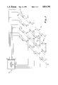
- FIG. 1 is an isometric view of a touch pad, partially broken away.
- FIG. 2 is an enlarged cross-sectional view (at 2--2 in FIG. 1) of the pad sandwich of the pad of FIG. 1, not to scale.
- FIG. 3 is an equivalent circuit diagram corresponding to a representative portion of the pad sandwich and related electronics.
- FIG. 4 is a block diagram of the control circuitry of FIG. 3.
- touch pad 10 has a large (e.g., 81/2" ⁇ 11") exposed resilient writing surface 12 for writing with a finger or stylus 15.
- surface 12 is part of a pad sandwich 14 which includes a flexible, resilient, transparent plastic upper layer 30 spaced apart (e.g., with a spacing of 5 microns) from and parallel to a flexible plastic lower layer 32 to define a cavity 34 between them.
- a conventional liquid crystal material is held within the cavity by sealing together the upper and lower layers 30, 32 along the peripheral edges of sandwich 14 (not shown).
- the flexibility and resilience of layer 30 are such that pressing at a point on the surface (e.g., 17) will deform layer 30 in a localized region at the point of pressure, with the deformed region returning to its original position after the pressing stops.
- Layers 30, 32 are kept spaced apart either by a matrix of resilient supporting pillars inserted between them or by selection of a liquid crystal material having appropriate physical characteristics.
- the bottom surface 36 of layer 30 is imprinted (by conventional thin-film technology) with a series of closely spaced (e.g., with a spacing of 0.005"), parallel, transparent, conductors 38 of a kind conventionally used in LCD displays.
- the top surface 40 of layer 32 is likewise imprinted with a series of closely spaced (e.g., with a spacing of 0.010"), parallel, transparent conductors 42. Only one conductor 42 appears on FIG. 2.
- Conductors 42 run along the length of pad 10 and conductors 38 along its width, thus forming a grid defining a matrix of pixels (display elements) on surface 12, each pixel being defined by the intersecting pair of conductors 38, 42 which underlie that pixel.
- pixel 44 is defined by a particular conductor 46 of the conductors 38, and a particular one of the conductors 42.
- conductors 42 can be viewed as forming rows and conductors 38 as forming columns in an equivalent circuit diagram.
- an imaginary discrete circuit element 50 which represents the electrical characteristic of a localized path between the particular row and column conductors 38, 42, associated with that pixel.
- the electrical characteristic of each such element 50 is indicated (by means of an arrow) as variable to reflect the fact that when surface 12 is depressed at a pixel location, the resulting local physical deformation of layer 30 with respect to layer 32 will produce a change in the electrical characteristic.
- the resulting localized reduction in distance between layers 30, 32 may increase the capacitance or decrease the resistance (or a combination of the two) between the associated top and bottom conductors 38, 42 depending on the materials and physical construction of pad 10.
- the electrical change in the local path between conductors 38, 42 may be called a change in conductance.
- each row conductor 42 is connected to a conventional source driver 52 (e.g., type HD44780 or HD44100 available from Hitachi) for feeding current to the conductor.
- the source drivers 52 are all connected to control circuitry 54 for selectively triggering appropriate ones of the drivers 52.
- Control circuitry 54 is also connected to a set of conventional sink display drivers 56 (e.g., type HD44100H or HD44780 available from Hitachi).
- Each sink display driver 56 is in turn connected to one of the column conductors 38 for sinking current from the corresponding conductor when triggered by control circuitry 54.
- control circuitry 54 is also connected to a set of input sensors 60 (e.g., type MC14049UB available from Motorola). Each input sensor 60 is in turn connected to one of the column conductors 38 for sensing an electrical value related to the conductance of various ones of the elements 50 connected to the conductor, such conductances being indicative of which elements 50 are being subjected to pressure.
- Each sensor 60 can be of the type having CMOS inverter gates which detect whether the sensed voltage appearing across an element 50 as a result of the pressure of stylus 15 is greater than a threshold voltage of the gate.
- Each sensor 60 also includes a voltage comparator circuit (e.g., type ⁇ A3302 available from Fairchild) for allowing the detection of differential voltage levels, for a purpose discussed below.
- control circuitry 54 includes a column selector which accepts bits from particular sensors 60 (indicating which elements 50 are being subjected to pressure) and delivers display bits to sink drivers 56 (corresponding to an image to be displayed) as dictated by trigger signals provided from an interlace controller 72. Any output bit from a selected sensor 60 is passed from column selector 70 back to controller 72.
- Control circuitry 54 also includes a row selector 74 which delivers display bits to source drivers 52 likewise based on trigger signals from controller 72. Controller 72 interleaves the displaying of pixels of an image specified by the data processor with the reading of entered information which is passed back to the data processor, all via line 22.
- the source drivers 52, sink display drivers 56, control circuitry 54, and sensors 60 are all included in electronic circuitry 18, mounted in housing 16. Conductors 38 and 42 are connected via leads 20 to circuitry 18.
- a cable 22 enables control circuitry 54 to send and receive information bits to and from the data processor, corresponding to pixels which are to be displayed or input information which is to be read.
- the pad is capable of simultaneously displaying output information from a data processor and receiving input information represented by pressure of stylus 15 at various points on surface 12 (e.g., the points along a line 62, FIG. 1).
- Displaying an image is accomplished in the conventional way for LCDs.
- Each of the pixels corresponding to the output information is darkened by establishing an electrical field across the liquid crystal material between the two conductors associated with that pixel.
- the field is established by triggering the corresponding source and sink drivers 52, 56.
- the field temporarily alters the molecular alignment of the liquid crystal material at the pixel, causing it to appear darker.
- An entire image is generated by rapidly triggering in succession (that is, scanning) the appropriate sink display drivers 56 while one of the source drivers 52 is triggered, then repeating the process while another one of the other source drivers is triggered, and so on. By repeating the scanning process (refreshing the image) at a high rate of repetition, the image is seen without interruption.
- controller 72 concurrently interlaces the displaying of pixels 44 with the reading of elements 50 in order to accomplish both in about the same time that would otherwise be required for displaying alone.
- the concurrent interlacing is accomplished as follows. First a given row conductor 42 is activated by triggering the corresponding driver 52. While that row conductor 42 is activated, each sensor 60 is triggered in turn to read the elements 50 along row conductor 42. If a pixel 44 is also to be displayed at the same intersection between the active row conductor 42, and the column conductor 38 associated with the triggered sensor 60, then the corresponding sink driver 56 is triggered at the same time; if that pixel is not to be displayed, that corresponding sink driver is not triggered. Sensor 60 is arranged to sense pressure at the element 50 corresponding to that pixel whether or not that pixel is simultaneously being displayed.
- the field used to cause the display may itself induce changes in the conductance of the corresponding element 50 similar to the changes produced by pressure on that element.
- the output of the source driver 52 is then used as an input to the voltage comparator circuit of sensor 60 to offset the effect of the drive voltage, thus permitting the sensor to detect that element 50 is being pressed.
- the displayed information can be the same as, or different from, the input information.
- the pad allows the user to see immediately on the pad what he has just written.
- the device is thin enough to sit conveniently on a desk top with the writing surface facing up. Information can be entered and displayed at the same time without flickering of the image.
- the interlacing can be accomplished by an offset technique in which the triggered sensor 60 is in the adjacent column to the column in which the sink driver 56 is potentially triggered.
- the sensors 60 will always be sensing elements 50 corresponding to undisplayed pixels.
- the total scanning time required for both image displaying and reading will be one column longer in duration for each row scanned because of the offsetting of the reading and displaying operations.
- the multiple sensors 60 could be replaced by a single sensor connected via a multiplexing switch (e.g., type MC14051B available from Motorola) to each of the columns to be sensed.
- the multiplexing switch would then be controlled by control circuitry 54.
Abstract
Description
Claims (9)
Priority Applications (1)
| Application Number | Priority Date | Filing Date | Title |
|---|---|---|---|
| US07/045,732 US4814760A (en) | 1984-12-28 | 1987-04-30 | Information display and entry device |
Applications Claiming Priority (2)
| Application Number | Priority Date | Filing Date | Title |
|---|---|---|---|
| US68707084A | 1984-12-28 | 1984-12-28 | |
| US07/045,732 US4814760A (en) | 1984-12-28 | 1987-04-30 | Information display and entry device |
Related Parent Applications (1)
| Application Number | Title | Priority Date | Filing Date |
|---|---|---|---|
| US68707084A Continuation | 1984-12-28 | 1984-12-28 |
Publications (1)
| Publication Number | Publication Date |
|---|---|
| US4814760A true US4814760A (en) | 1989-03-21 |
Family
ID=26723137
Family Applications (1)
| Application Number | Title | Priority Date | Filing Date |
|---|---|---|---|
| US07/045,732 Expired - Fee Related US4814760A (en) | 1984-12-28 | 1987-04-30 | Information display and entry device |
Country Status (1)
| Country | Link |
|---|---|
| US (1) | US4814760A (en) |
Cited By (79)
| Publication number | Priority date | Publication date | Assignee | Title |
|---|---|---|---|---|
| US4980646A (en) * | 1988-03-30 | 1990-12-25 | The Trustees Of The University Of Pennsylvania | Impedance tomographic tactile sensor |
| US5111316A (en) * | 1990-08-09 | 1992-05-05 | Western Publishing Company | Liquid crystal writing state |
| US5115330A (en) * | 1990-08-09 | 1992-05-19 | Western Publishing Company | Liquid crystal writing slate |
| US5117297A (en) * | 1990-08-09 | 1992-05-26 | Western Publishing Company | Liquid crystal writing slate with DC imaging system |
| US5136404A (en) * | 1990-08-09 | 1992-08-04 | Western Publishing Company | Liquid crystal writing slate with improved light-transmission retention |
| US5194852A (en) * | 1986-12-01 | 1993-03-16 | More Edward S | Electro-optic slate for direct entry and display and/or storage of hand-entered textual and graphic information |
| US5241308A (en) * | 1990-02-22 | 1993-08-31 | Paragon Systems, Inc. | Force sensitive touch panel |
| US5272470A (en) * | 1991-10-10 | 1993-12-21 | International Business Machines Corporation | Apparatus and method for reducing system overhead while inking strokes in a finger or stylus-based input device of a data processing system |
| US5369228A (en) * | 1991-11-30 | 1994-11-29 | Signagraphics Corporation | Data input device with a pressure-sensitive input surface |
| US5392058A (en) * | 1991-05-15 | 1995-02-21 | Sharp Kabushiki Kaisha | Display-integrated type tablet device |
| US5400054A (en) * | 1991-07-12 | 1995-03-21 | Dorst; Gary L. | Manually operable device for indicating position on a display screen |
| US5446480A (en) * | 1989-08-17 | 1995-08-29 | Sony Corporation | Input device for entering data for electronic equipments and so forth |
| WO1996005550A1 (en) * | 1994-08-12 | 1996-02-22 | Philips Electronics N.V. | Data processing system comprising a user interface |
| US5508720A (en) * | 1994-02-02 | 1996-04-16 | Copytele, Inc. | Portable telecommunication device with removable electrophoretic display |
| US5528266A (en) * | 1989-05-15 | 1996-06-18 | International Business Machines Corporation | Flat touch screen workpad for a data processing system |
| US5541372A (en) * | 1992-06-15 | 1996-07-30 | U.S. Philips Corporation | Force activated touch screen measuring deformation of the front panel |
| US5565892A (en) * | 1991-12-24 | 1996-10-15 | Ncr Corporation | Display and data entry device and method for manufacturing the same |
| US5610629A (en) * | 1991-12-06 | 1997-03-11 | Ncr Corporation | Pen input to liquid crystal display |
| US5631805A (en) * | 1995-09-27 | 1997-05-20 | Dynapro Systems, Inc. | Touch screen enclosure having an insertable graphic sheet |
| US5636101A (en) * | 1995-09-27 | 1997-06-03 | Dynapro Systems, Inc. | Touch screen enclosure system having touch screen pan and hinged rear enclosure section for ease of serviceability |
| US5640296A (en) * | 1995-09-27 | 1997-06-17 | Dynapro Systems, Inc. | Touch screen enclosure having a universal rear enclosure unit, a touch screen plate, and first and second seals |
| US5652412A (en) * | 1994-07-11 | 1997-07-29 | Sia Technology Corp. | Pen and paper information recording system |
| US5661506A (en) * | 1994-11-10 | 1997-08-26 | Sia Technology Corporation | Pen and paper information recording system using an imaging pen |
| US5751453A (en) * | 1991-12-06 | 1998-05-12 | Ncr Corporation | Liquid crystal display with pen-input capability |
| US5990865A (en) * | 1997-01-06 | 1999-11-23 | Gard; Matthew Davis | Computer interface device |
| US6014132A (en) * | 1990-11-20 | 2000-01-11 | Canon Kabushiki Kaisha | Electronic device |
| US6134392A (en) * | 1991-09-26 | 2000-10-17 | Texas Instruments Incorporated | Camera with user operable input device |
| US6173045B1 (en) * | 1991-06-27 | 2001-01-09 | Texas Instruments Incorporated | Electronic telephone book |
| US20020122123A1 (en) * | 2001-03-01 | 2002-09-05 | Semiconductor Energy Laboratory Co., Ltd. | Defective pixel specifying method, defective pixel specifying system, image correcting method, and image correcting system |
| US6539363B1 (en) * | 1990-08-30 | 2003-03-25 | Ncr Corporation | Write input credit transaction apparatus and method with paperless merchant credit card processing |
| US20030156087A1 (en) * | 2002-02-20 | 2003-08-21 | Boer Willem Den | Light sensitive display |
| US20030218116A1 (en) * | 2002-02-20 | 2003-11-27 | Boer Willem Den | Image sensor with photosensitive thin film transistors |
| WO2004001662A2 (en) * | 2002-06-25 | 2003-12-31 | 3M Innovative Properties Company | Touch sensor |
| WO2004013746A2 (en) * | 2002-08-01 | 2004-02-12 | Koninklijke Philips Electronics N.V. | Touch sensitive display device |
| US20040107369A1 (en) * | 2002-11-30 | 2004-06-03 | Barnes Cooper | Apparatus and method for multi-threaded processors performance control |
| WO2004066136A2 (en) * | 2003-01-20 | 2004-08-05 | Koninklijke Philips Electronics N.V. | Touch sensitive display device |
| US20040155991A1 (en) * | 2002-11-21 | 2004-08-12 | Lowles Robert J. | System and method of integrating a touchscreen within an LCD |
| US20050110780A1 (en) * | 1989-07-03 | 2005-05-26 | Ditzik Richard J. | Desktop computer conferencing system |
| US20050116020A1 (en) * | 2003-11-07 | 2005-06-02 | Smolucha Walter E. | Locating individuals and games in a gaming establishment |
| US20050122119A1 (en) * | 2003-12-05 | 2005-06-09 | Touchram Llc | Low noise proximity sensing system |
| US20050134751A1 (en) * | 2003-12-17 | 2005-06-23 | Adiel Abileah | Light sensitive display |
| US20050134749A1 (en) * | 2003-12-19 | 2005-06-23 | Adiel Abileah | Reflection resistant display |
| US20050184552A1 (en) * | 2004-02-19 | 2005-08-25 | Lear Corporation | Erasable message board for a vehicle |
| US20050231656A1 (en) * | 2004-04-16 | 2005-10-20 | Planar Systems, Inc. | Image sensor with photosensitive thin film transistors and dark current compensation |
| WO2005101178A2 (en) * | 2004-04-14 | 2005-10-27 | Koninklijke Philips Electronics N.V. | Touch sensitive display |
| US7053967B2 (en) | 2002-05-23 | 2006-05-30 | Planar Systems, Inc. | Light sensitive display |
| US20060187029A1 (en) * | 2005-02-24 | 2006-08-24 | Alfred Thomas | Security zones for casino gaming |
| US20060258442A1 (en) * | 2005-05-13 | 2006-11-16 | Ryan Chad A | Multi-purpose casino chips |
| US20060287078A1 (en) * | 2004-04-22 | 2006-12-21 | Smolucha Walter E | Identifying components of a casino game |
| US20070109239A1 (en) * | 2005-11-14 | 2007-05-17 | Den Boer Willem | Integrated light sensitive liquid crystal display |
| US20080048995A1 (en) * | 2003-02-20 | 2008-02-28 | Planar Systems, Inc. | Light sensitive display |
| US20080062156A1 (en) * | 2003-02-20 | 2008-03-13 | Planar Systems, Inc. | Light sensitive display |
| US20080316231A1 (en) * | 2007-06-19 | 2008-12-25 | Raman Research Institute | Method and System for Line By Line Addressing of RMS Responding Display Matrix with Wavelets |
| US20090167712A1 (en) * | 2002-03-01 | 2009-07-02 | Planar Systems, Inc. | Reflection resistant touch screens |
| US20100079400A1 (en) * | 2008-09-26 | 2010-04-01 | Sony Ericsson Mobile Communications Ab | Touch sensitive display with conductive liquid |
| US20100188345A1 (en) * | 2009-01-23 | 2010-07-29 | Mustafa Keskin | Conductive multi-touch touch panel |
| US20110109566A1 (en) * | 2009-11-12 | 2011-05-12 | Innocom Technology (Shenzhen) Co., Ltd. | Touch panel with pdlc film and touch-sensitive display device using same |
| US20120044190A1 (en) * | 2010-08-20 | 2012-02-23 | Qrg Limited | Electronic ink touch sensitive display |
| WO2012050445A1 (en) | 2010-10-13 | 2012-04-19 | Polymer Vision B.V. | Common driving of displays |
| WO2012078042A2 (en) | 2010-12-08 | 2012-06-14 | Polymer Vision B.V. | Consecutive driving of displays |
| WO2012099468A1 (en) | 2011-01-19 | 2012-07-26 | Polymer Vision B.V. | Super low voltage driving of displays |
| US8638320B2 (en) | 2011-06-22 | 2014-01-28 | Apple Inc. | Stylus orientation detection |
| US8928635B2 (en) | 2011-06-22 | 2015-01-06 | Apple Inc. | Active stylus |
| US9176604B2 (en) | 2012-07-27 | 2015-11-03 | Apple Inc. | Stylus device |
| US9244559B2 (en) | 2012-12-14 | 2016-01-26 | Atmel Corporation | Integrated pixel display and touch sensor |
| USD749566S1 (en) * | 2014-02-19 | 2016-02-16 | Fujifilm Corporation | Personal digital assistance |
| US9310923B2 (en) | 2010-12-03 | 2016-04-12 | Apple Inc. | Input device for touch sensitive devices |
| US9329703B2 (en) | 2011-06-22 | 2016-05-03 | Apple Inc. | Intelligent stylus |
| USD755785S1 (en) * | 2014-08-04 | 2016-05-10 | Smart Technologies Ulc | Interactive board |
| US9557845B2 (en) | 2012-07-27 | 2017-01-31 | Apple Inc. | Input device for and method of communication with capacitive devices through frequency variation |
| USD784452S1 (en) * | 2016-01-21 | 2017-04-18 | Handwriting Tree, LLC | Board |
| USD784451S1 (en) * | 2016-01-21 | 2017-04-18 | Handwriting Tree, LLC | Board |
| US9652090B2 (en) | 2012-07-27 | 2017-05-16 | Apple Inc. | Device for digital communication through capacitive coupling |
| US9939935B2 (en) | 2013-07-31 | 2018-04-10 | Apple Inc. | Scan engine for touch controller architecture |
| US10048775B2 (en) | 2013-03-14 | 2018-08-14 | Apple Inc. | Stylus detection and demodulation |
| US10061450B2 (en) | 2014-12-04 | 2018-08-28 | Apple Inc. | Coarse scan and targeted active mode scan for touch |
| USD827600S1 (en) * | 2017-01-17 | 2018-09-04 | Albert L. J. Lammens | Bathroom television |
| US10474277B2 (en) | 2016-05-31 | 2019-11-12 | Apple Inc. | Position-based stylus communication |
| USD918854S1 (en) * | 2019-04-25 | 2021-05-11 | Lg Electronics Inc. | Television with rollable display |
Citations (24)
| Publication number | Priority date | Publication date | Assignee | Title |
|---|---|---|---|---|
| US3816824A (en) * | 1972-02-18 | 1974-06-11 | Philips Corp | Method and arrangement for optically displaying characters constituted by raster light spots on a projection surface |
| US4017848A (en) * | 1975-05-19 | 1977-04-12 | Rockwell International Corporation | Transparent keyboard switch and array |
| US4078257A (en) * | 1976-08-23 | 1978-03-07 | Hewlett-Packard Company | Calculator apparatus with electronically alterable key symbols |
| JPS5372422A (en) * | 1976-12-08 | 1978-06-27 | Sharp Corp | Input unit |
| JPS54119899A (en) * | 1978-03-10 | 1979-09-18 | Hitachi Ltd | Liquid crystal display unit |
| US4177354A (en) * | 1978-04-17 | 1979-12-04 | Bell Telephone Laboratories, Incorporated | Graphic communications apparatus |
| GB2026745A (en) * | 1978-07-28 | 1980-02-06 | Burroughs Corp | Touch panel and operating system |
| JPS5583922A (en) * | 1978-12-21 | 1980-06-24 | Casio Comput Co Ltd | Key input device |
| US4224615A (en) * | 1978-09-14 | 1980-09-23 | Texas Instruments Incorporated | Method of using a liquid crystal display device as a data input device |
| US4290061A (en) * | 1979-08-23 | 1981-09-15 | General Electric Company | Electrically integrated touch input and output display system |
| US4303916A (en) * | 1978-08-31 | 1981-12-01 | Sharp Kabushiki Kaisha | Multi-item input/output device to input information to and retrieve other information from a terminal computer |
| US4334219A (en) * | 1979-02-28 | 1982-06-08 | Agfa-Gevaert Ag | Operation setting device having stationary touch-sensitive control elements |
| US4345248A (en) * | 1979-12-14 | 1982-08-17 | Citizen Watch Company Limited | Liquid crystal display device with write-in capability |
| US4367465A (en) * | 1980-04-04 | 1983-01-04 | Hewlett-Packard Company | Graphics light pen and method for raster scan CRT |
| US4371893A (en) * | 1979-09-11 | 1983-02-01 | Rabeisen Andre J | Video communication system allowing graphic additions to the images communicated |
| US4377810A (en) * | 1980-12-04 | 1983-03-22 | Data General Corporation | Light pen detection circuit and method |
| US4405921A (en) * | 1980-05-12 | 1983-09-20 | Kabushiki Kaisha Suwa Seikosha | Liquid crystal display device |
| JPS5935277A (en) * | 1982-08-23 | 1984-02-25 | Nippon Telegr & Teleph Corp <Ntt> | Controlling method by real-time recognition of handwritten character pattern |
| US4475239A (en) * | 1981-07-08 | 1984-10-02 | Olympia Werke Ag | Apparatus for text editing and processing |
| US4475161A (en) * | 1980-04-11 | 1984-10-02 | Ampex Corporation | YIQ Computer graphics system |
| US4520357A (en) * | 1982-07-23 | 1985-05-28 | General Electric Company | Electroscopic information display and entry system with writing stylus |
| US4567480A (en) * | 1982-12-13 | 1986-01-28 | John Fluke Mfg. Co., Inc. | Touch-sensitive overlay |
| US4630039A (en) * | 1981-09-21 | 1986-12-16 | Nippon Electric Co., Ltd. | Display processing apparatus |
| US4639720A (en) * | 1981-01-12 | 1987-01-27 | Harris Corporation | Electronic sketch pad |
-
1987
- 1987-04-30 US US07/045,732 patent/US4814760A/en not_active Expired - Fee Related
Patent Citations (24)
| Publication number | Priority date | Publication date | Assignee | Title |
|---|---|---|---|---|
| US3816824A (en) * | 1972-02-18 | 1974-06-11 | Philips Corp | Method and arrangement for optically displaying characters constituted by raster light spots on a projection surface |
| US4017848A (en) * | 1975-05-19 | 1977-04-12 | Rockwell International Corporation | Transparent keyboard switch and array |
| US4078257A (en) * | 1976-08-23 | 1978-03-07 | Hewlett-Packard Company | Calculator apparatus with electronically alterable key symbols |
| JPS5372422A (en) * | 1976-12-08 | 1978-06-27 | Sharp Corp | Input unit |
| JPS54119899A (en) * | 1978-03-10 | 1979-09-18 | Hitachi Ltd | Liquid crystal display unit |
| US4177354A (en) * | 1978-04-17 | 1979-12-04 | Bell Telephone Laboratories, Incorporated | Graphic communications apparatus |
| GB2026745A (en) * | 1978-07-28 | 1980-02-06 | Burroughs Corp | Touch panel and operating system |
| US4303916A (en) * | 1978-08-31 | 1981-12-01 | Sharp Kabushiki Kaisha | Multi-item input/output device to input information to and retrieve other information from a terminal computer |
| US4224615A (en) * | 1978-09-14 | 1980-09-23 | Texas Instruments Incorporated | Method of using a liquid crystal display device as a data input device |
| JPS5583922A (en) * | 1978-12-21 | 1980-06-24 | Casio Comput Co Ltd | Key input device |
| US4334219A (en) * | 1979-02-28 | 1982-06-08 | Agfa-Gevaert Ag | Operation setting device having stationary touch-sensitive control elements |
| US4290061A (en) * | 1979-08-23 | 1981-09-15 | General Electric Company | Electrically integrated touch input and output display system |
| US4371893A (en) * | 1979-09-11 | 1983-02-01 | Rabeisen Andre J | Video communication system allowing graphic additions to the images communicated |
| US4345248A (en) * | 1979-12-14 | 1982-08-17 | Citizen Watch Company Limited | Liquid crystal display device with write-in capability |
| US4367465A (en) * | 1980-04-04 | 1983-01-04 | Hewlett-Packard Company | Graphics light pen and method for raster scan CRT |
| US4475161A (en) * | 1980-04-11 | 1984-10-02 | Ampex Corporation | YIQ Computer graphics system |
| US4405921A (en) * | 1980-05-12 | 1983-09-20 | Kabushiki Kaisha Suwa Seikosha | Liquid crystal display device |
| US4377810A (en) * | 1980-12-04 | 1983-03-22 | Data General Corporation | Light pen detection circuit and method |
| US4639720A (en) * | 1981-01-12 | 1987-01-27 | Harris Corporation | Electronic sketch pad |
| US4475239A (en) * | 1981-07-08 | 1984-10-02 | Olympia Werke Ag | Apparatus for text editing and processing |
| US4630039A (en) * | 1981-09-21 | 1986-12-16 | Nippon Electric Co., Ltd. | Display processing apparatus |
| US4520357A (en) * | 1982-07-23 | 1985-05-28 | General Electric Company | Electroscopic information display and entry system with writing stylus |
| JPS5935277A (en) * | 1982-08-23 | 1984-02-25 | Nippon Telegr & Teleph Corp <Ntt> | Controlling method by real-time recognition of handwritten character pattern |
| US4567480A (en) * | 1982-12-13 | 1986-01-28 | John Fluke Mfg. Co., Inc. | Touch-sensitive overlay |
Cited By (169)
| Publication number | Priority date | Publication date | Assignee | Title |
|---|---|---|---|---|
| US5194852A (en) * | 1986-12-01 | 1993-03-16 | More Edward S | Electro-optic slate for direct entry and display and/or storage of hand-entered textual and graphic information |
| US4980646A (en) * | 1988-03-30 | 1990-12-25 | The Trustees Of The University Of Pennsylvania | Impedance tomographic tactile sensor |
| US5528266A (en) * | 1989-05-15 | 1996-06-18 | International Business Machines Corporation | Flat touch screen workpad for a data processing system |
| US20050110780A1 (en) * | 1989-07-03 | 2005-05-26 | Ditzik Richard J. | Desktop computer conferencing system |
| US20060097999A1 (en) * | 1989-07-03 | 2006-05-11 | Ditzik Richard J | Desktop computer conferencing system |
| US20060097998A1 (en) * | 1989-07-03 | 2006-05-11 | Ditzik Richard J | Desktop computer conferencing system |
| US5446480A (en) * | 1989-08-17 | 1995-08-29 | Sony Corporation | Input device for entering data for electronic equipments and so forth |
| US5241308A (en) * | 1990-02-22 | 1993-08-31 | Paragon Systems, Inc. | Force sensitive touch panel |
| US5111316A (en) * | 1990-08-09 | 1992-05-05 | Western Publishing Company | Liquid crystal writing state |
| US5115330A (en) * | 1990-08-09 | 1992-05-19 | Western Publishing Company | Liquid crystal writing slate |
| US5117297A (en) * | 1990-08-09 | 1992-05-26 | Western Publishing Company | Liquid crystal writing slate with DC imaging system |
| US5136404A (en) * | 1990-08-09 | 1992-08-04 | Western Publishing Company | Liquid crystal writing slate with improved light-transmission retention |
| US6539363B1 (en) * | 1990-08-30 | 2003-03-25 | Ncr Corporation | Write input credit transaction apparatus and method with paperless merchant credit card processing |
| US6014132A (en) * | 1990-11-20 | 2000-01-11 | Canon Kabushiki Kaisha | Electronic device |
| US5392058A (en) * | 1991-05-15 | 1995-02-21 | Sharp Kabushiki Kaisha | Display-integrated type tablet device |
| US6173045B1 (en) * | 1991-06-27 | 2001-01-09 | Texas Instruments Incorporated | Electronic telephone book |
| US5473345A (en) * | 1991-07-12 | 1995-12-05 | Dorst; Gary L. | Device incorporating a mouse, for indicating position on a display screen |
| US5400054A (en) * | 1991-07-12 | 1995-03-21 | Dorst; Gary L. | Manually operable device for indicating position on a display screen |
| US6134392A (en) * | 1991-09-26 | 2000-10-17 | Texas Instruments Incorporated | Camera with user operable input device |
| US5272470A (en) * | 1991-10-10 | 1993-12-21 | International Business Machines Corporation | Apparatus and method for reducing system overhead while inking strokes in a finger or stylus-based input device of a data processing system |
| US5369228A (en) * | 1991-11-30 | 1994-11-29 | Signagraphics Corporation | Data input device with a pressure-sensitive input surface |
| US5610629A (en) * | 1991-12-06 | 1997-03-11 | Ncr Corporation | Pen input to liquid crystal display |
| US5751453A (en) * | 1991-12-06 | 1998-05-12 | Ncr Corporation | Liquid crystal display with pen-input capability |
| US5565892A (en) * | 1991-12-24 | 1996-10-15 | Ncr Corporation | Display and data entry device and method for manufacturing the same |
| US5541372A (en) * | 1992-06-15 | 1996-07-30 | U.S. Philips Corporation | Force activated touch screen measuring deformation of the front panel |
| US5508720A (en) * | 1994-02-02 | 1996-04-16 | Copytele, Inc. | Portable telecommunication device with removable electrophoretic display |
| US5652412A (en) * | 1994-07-11 | 1997-07-29 | Sia Technology Corp. | Pen and paper information recording system |
| WO1996005550A1 (en) * | 1994-08-12 | 1996-02-22 | Philips Electronics N.V. | Data processing system comprising a user interface |
| US5661506A (en) * | 1994-11-10 | 1997-08-26 | Sia Technology Corporation | Pen and paper information recording system using an imaging pen |
| US5640296A (en) * | 1995-09-27 | 1997-06-17 | Dynapro Systems, Inc. | Touch screen enclosure having a universal rear enclosure unit, a touch screen plate, and first and second seals |
| US5631805A (en) * | 1995-09-27 | 1997-05-20 | Dynapro Systems, Inc. | Touch screen enclosure having an insertable graphic sheet |
| US5636101A (en) * | 1995-09-27 | 1997-06-03 | Dynapro Systems, Inc. | Touch screen enclosure system having touch screen pan and hinged rear enclosure section for ease of serviceability |
| US5990865A (en) * | 1997-01-06 | 1999-11-23 | Gard; Matthew Davis | Computer interface device |
| US7333089B1 (en) | 1997-01-06 | 2008-02-19 | Matthew Davis Gard | Computer interface device |
| US20080297628A1 (en) * | 2001-03-01 | 2008-12-04 | Semiconductor Energy Laboratory Co., Ltd. | Defective pixel specifying method, defective pixel specifying system, image correcting method, and image correcting system |
| US20100253813A1 (en) * | 2001-03-01 | 2010-10-07 | Semiconductor Energy Laboratory Co., Ltd. | Defective pixel specifying method, defective pixel specifying system, image correcting method, and image correcting system |
| US7683949B2 (en) * | 2001-03-01 | 2010-03-23 | Semiconductor Energy Laboratory Co., Ltd | Defective pixel specifying method, defective pixel specifying system, image correcting method, and image correcting system |
| US20060280377A1 (en) * | 2001-03-01 | 2006-12-14 | Semiconductor Energy Laboratory Co., Ltd. | Defective pixel specifying method, defective pixel specifying system, image correcting method, and image correcting system |
| US7102673B2 (en) * | 2001-03-01 | 2006-09-05 | Semiconductor Energy Laboratory Co., Ltd. | Defective pixel specifying method, defective pixel specifying system, image correcting method, and image correcting system |
| US20110058074A1 (en) * | 2001-03-01 | 2011-03-10 | Semiconductor Energy Laboratory Co., Ltd. | Defective pixel specifying method, defective pixel specifying system, image correcting method, and image correcting system |
| US7969489B2 (en) * | 2001-03-01 | 2011-06-28 | Semiconductor Energy Laboratory Co., Ltd. | Defective pixel specifying method, defective pixel specifying system, image correcting method, and image correcting system |
| US7417676B2 (en) * | 2001-03-01 | 2008-08-26 | Semiconductor Energy Laboratory Co., Ltd. | Defective pixel specifying method, defective pixel specifying system, image correcting method, and image correcting system |
| US8385682B2 (en) | 2001-03-01 | 2013-02-26 | Semiconductor Energy Laboratory Co., Ltd. | Defective pixel specifying method, defective pixel specifying system, image correcting method, and image correcting system |
| US8130291B2 (en) * | 2001-03-01 | 2012-03-06 | Semiconductor Energy Laboratory Co., Ltd. | Defective pixel specifying method, defective pixel specifying system, image correcting method, and image correcting system |
| US20020122123A1 (en) * | 2001-03-01 | 2002-09-05 | Semiconductor Energy Laboratory Co., Ltd. | Defective pixel specifying method, defective pixel specifying system, image correcting method, and image correcting system |
| US6947102B2 (en) | 2002-02-20 | 2005-09-20 | Plannar Systems, Inc. | Light sensitive display which senses decreases in light |
| US20030218116A1 (en) * | 2002-02-20 | 2003-11-27 | Boer Willem Den | Image sensor with photosensitive thin film transistors |
| US9411470B2 (en) | 2002-02-20 | 2016-08-09 | Apple Inc. | Light sensitive display with multiple data set object detection |
| US20100013794A1 (en) * | 2002-02-20 | 2010-01-21 | Apple Inc. | Light sensitive display with multiple data set object detection |
| US9134851B2 (en) | 2002-02-20 | 2015-09-15 | Apple Inc. | Light sensitive display |
| US20100013793A1 (en) * | 2002-02-20 | 2010-01-21 | Apple Inc. | Light sensitive display with pressure sensor |
| US20100013796A1 (en) * | 2002-02-20 | 2010-01-21 | Apple Inc. | Light sensitive display with object detection calibration |
| US8570449B2 (en) | 2002-02-20 | 2013-10-29 | Apple Inc. | Light sensitive display with pressure sensor |
| US8441422B2 (en) | 2002-02-20 | 2013-05-14 | Apple Inc. | Light sensitive display with object detection calibration |
| US11073926B2 (en) | 2002-02-20 | 2021-07-27 | Apple Inc. | Light sensitive display |
| US20050285985A1 (en) * | 2002-02-20 | 2005-12-29 | Planar Systems, Inc. | Light sensitive display |
| US6995743B2 (en) | 2002-02-20 | 2006-02-07 | Planar Systems, Inc. | Light sensitive display |
| US20100020044A1 (en) * | 2002-02-20 | 2010-01-28 | Apple Inc. | Light sensitive display with switchable detection modes |
| US7023503B2 (en) | 2002-02-20 | 2006-04-04 | Planar Systems, Inc. | Image sensor with photosensitive thin film transistors |
| US20100059296A9 (en) * | 2002-02-20 | 2010-03-11 | Planar Systems, Inc. | Light sensitive display |
| US20030156087A1 (en) * | 2002-02-20 | 2003-08-21 | Boer Willem Den | Light sensitive display |
| US20030179323A1 (en) * | 2002-02-20 | 2003-09-25 | Adiel Abileah | Light sensitive display |
| US7408598B2 (en) | 2002-02-20 | 2008-08-05 | Planar Systems, Inc. | Light sensitive display with selected interval of light sensitive elements |
| US20080129914A1 (en) * | 2002-02-20 | 2008-06-05 | Planar Systems, Inc. | Light sensitive display |
| US20080129909A1 (en) * | 2002-02-20 | 2008-06-05 | Planar Systems, Inc. | Light sensitive display |
| US20080129913A1 (en) * | 2002-02-20 | 2008-06-05 | Planar Systems, Inc. | Light sensitive display |
| US20080111780A1 (en) * | 2002-02-20 | 2008-05-15 | Planar Systems, Inc. | Light sensitive display |
| US9971456B2 (en) | 2002-02-20 | 2018-05-15 | Apple Inc. | Light sensitive display with switchable detection modes for detecting a fingerprint |
| US20080066972A1 (en) * | 2002-02-20 | 2008-03-20 | Planar Systems, Inc. | Light sensitive display |
| US20080062343A1 (en) * | 2002-02-20 | 2008-03-13 | Planar Systems, Inc. | Light sensitive display |
| US20080055507A1 (en) * | 2002-02-20 | 2008-03-06 | Planar Systems, Inc. | Light sensitive display |
| US7872641B2 (en) | 2002-02-20 | 2011-01-18 | Apple Inc. | Light sensitive display |
| US7280102B2 (en) | 2002-02-20 | 2007-10-09 | Planar Systems, Inc. | Light sensitive display |
| US20070279346A1 (en) * | 2002-02-20 | 2007-12-06 | Planar Systems, Inc. | Display with embedded image sensor |
| US20080055295A1 (en) * | 2002-02-20 | 2008-03-06 | Planar Systems, Inc. | Light sensitive display |
| US20040046900A1 (en) * | 2002-02-20 | 2004-03-11 | Boer Willem Den | Light sensitive display |
| US20090167712A1 (en) * | 2002-03-01 | 2009-07-02 | Planar Systems, Inc. | Reflection resistant touch screens |
| US20060187367A1 (en) * | 2002-05-23 | 2006-08-24 | Adiel Abileah | Light sensitive display |
| US20080165311A1 (en) * | 2002-05-23 | 2008-07-10 | Adiel Abileah | Light sensitive display |
| US20080049154A1 (en) * | 2002-05-23 | 2008-02-28 | Adiel Abileah | Light sensitive display |
| US7852417B2 (en) | 2002-05-23 | 2010-12-14 | Apple Inc. | Light sensitive display |
| US7830461B2 (en) | 2002-05-23 | 2010-11-09 | Apple Inc. | Light sensitive display |
| US7880733B2 (en) | 2002-05-23 | 2011-02-01 | Apple Inc. | Light sensitive display |
| US20080049153A1 (en) * | 2002-05-23 | 2008-02-28 | Adiel Abileah | Light sensitive display |
| US7880819B2 (en) | 2002-05-23 | 2011-02-01 | Apple Inc. | Light sensitive display |
| US9354735B2 (en) | 2002-05-23 | 2016-05-31 | Apple Inc. | Light sensitive display |
| US8044930B2 (en) | 2002-05-23 | 2011-10-25 | Apple Inc. | Light sensitive display |
| US7053967B2 (en) | 2002-05-23 | 2006-05-30 | Planar Systems, Inc. | Light sensitive display |
| WO2004001662A3 (en) * | 2002-06-25 | 2004-03-25 | 3M Innovative Properties Co | Touch sensor |
| WO2004001662A2 (en) * | 2002-06-25 | 2003-12-31 | 3M Innovative Properties Company | Touch sensor |
| WO2004013746A2 (en) * | 2002-08-01 | 2004-02-12 | Koninklijke Philips Electronics N.V. | Touch sensitive display device |
| WO2004013746A3 (en) * | 2002-08-01 | 2004-10-14 | Koninkl Philips Electronics Nv | Touch sensitive display device |
| US7205983B2 (en) * | 2002-08-01 | 2007-04-17 | Koninklijke Philips Electronics, N.V. | Touch sensitive display device |
| US20050231461A1 (en) * | 2002-08-01 | 2005-10-20 | Raap Adriaan Y | Touch sensitive display device |
| US20040155991A1 (en) * | 2002-11-21 | 2004-08-12 | Lowles Robert J. | System and method of integrating a touchscreen within an LCD |
| US7388571B2 (en) * | 2002-11-21 | 2008-06-17 | Research In Motion Limited | System and method of integrating a touchscreen within an LCD |
| WO2004046905A3 (en) * | 2002-11-21 | 2004-08-26 | Research In Motion Ltd | Device and method of integrating a touchscreen within an liquid crystal display |
| US20080030479A1 (en) * | 2002-11-21 | 2008-02-07 | Research In Motion Limited | System and method of integrating a touchscreen within an lcd |
| US20040107369A1 (en) * | 2002-11-30 | 2004-06-03 | Barnes Cooper | Apparatus and method for multi-threaded processors performance control |
| WO2004066136A2 (en) * | 2003-01-20 | 2004-08-05 | Koninklijke Philips Electronics N.V. | Touch sensitive display device |
| WO2004066136A3 (en) * | 2003-01-20 | 2004-12-16 | Koninkl Philips Electronics Nv | Touch sensitive display device |
| US20080062156A1 (en) * | 2003-02-20 | 2008-03-13 | Planar Systems, Inc. | Light sensitive display |
| US20080084374A1 (en) * | 2003-02-20 | 2008-04-10 | Planar Systems, Inc. | Light sensitive display |
| US8207946B2 (en) | 2003-02-20 | 2012-06-26 | Apple Inc. | Light sensitive display |
| US20080048995A1 (en) * | 2003-02-20 | 2008-02-28 | Planar Systems, Inc. | Light sensitive display |
| US20050116020A1 (en) * | 2003-11-07 | 2005-06-02 | Smolucha Walter E. | Locating individuals and games in a gaming establishment |
| US20050122119A1 (en) * | 2003-12-05 | 2005-06-09 | Touchram Llc | Low noise proximity sensing system |
| US20050134751A1 (en) * | 2003-12-17 | 2005-06-23 | Adiel Abileah | Light sensitive display |
| US7009663B2 (en) | 2003-12-17 | 2006-03-07 | Planar Systems, Inc. | Integrated optical light sensitive active matrix liquid crystal display |
| US20060125971A1 (en) * | 2003-12-17 | 2006-06-15 | Planar Systems, Inc. | Integrated optical light sensitive active matrix liquid crystal display |
| US20050134749A1 (en) * | 2003-12-19 | 2005-06-23 | Adiel Abileah | Reflection resistant display |
| US20050184552A1 (en) * | 2004-02-19 | 2005-08-25 | Lear Corporation | Erasable message board for a vehicle |
| US6971703B2 (en) * | 2004-02-19 | 2005-12-06 | Lear Corporation | Erasable message board for a vehicle |
| WO2005101178A2 (en) * | 2004-04-14 | 2005-10-27 | Koninklijke Philips Electronics N.V. | Touch sensitive display |
| WO2005101178A3 (en) * | 2004-04-14 | 2006-04-13 | Koninkl Philips Electronics Nv | Touch sensitive display |
| US20100302419A1 (en) * | 2004-04-16 | 2010-12-02 | Apple Inc. | Image sensor with photosensitive thin film transistors and dark current compensation |
| US20050231656A1 (en) * | 2004-04-16 | 2005-10-20 | Planar Systems, Inc. | Image sensor with photosensitive thin film transistors and dark current compensation |
| US7773139B2 (en) | 2004-04-16 | 2010-08-10 | Apple Inc. | Image sensor with photosensitive thin film transistors |
| US8289429B2 (en) | 2004-04-16 | 2012-10-16 | Apple Inc. | Image sensor with photosensitive thin film transistors and dark current compensation |
| US20060287078A1 (en) * | 2004-04-22 | 2006-12-21 | Smolucha Walter E | Identifying components of a casino game |
| US20060187029A1 (en) * | 2005-02-24 | 2006-08-24 | Alfred Thomas | Security zones for casino gaming |
| US7330108B2 (en) | 2005-02-24 | 2008-02-12 | Wms Gaming Inc. | Security zones for casino gaming |
| US20080096649A1 (en) * | 2005-02-24 | 2008-04-24 | Wms Gaming Inc. | Security zones for casino gaming |
| US7602298B2 (en) | 2005-02-24 | 2009-10-13 | Wms Gaming Inc. | Security zones for casino gaming |
| US20060258442A1 (en) * | 2005-05-13 | 2006-11-16 | Ryan Chad A | Multi-purpose casino chips |
| US20070109239A1 (en) * | 2005-11-14 | 2007-05-17 | Den Boer Willem | Integrated light sensitive liquid crystal display |
| US20080316231A1 (en) * | 2007-06-19 | 2008-12-25 | Raman Research Institute | Method and System for Line By Line Addressing of RMS Responding Display Matrix with Wavelets |
| US8115717B2 (en) * | 2007-06-19 | 2012-02-14 | Raman Research Institute | Method and system for line by line addressing of RMS responding display matrix with wavelets |
| US20100079400A1 (en) * | 2008-09-26 | 2010-04-01 | Sony Ericsson Mobile Communications Ab | Touch sensitive display with conductive liquid |
| US9342202B2 (en) * | 2009-01-23 | 2016-05-17 | Qualcomm Incorporated | Conductive multi-touch touch panel |
| US20100188345A1 (en) * | 2009-01-23 | 2010-07-29 | Mustafa Keskin | Conductive multi-touch touch panel |
| US20110109566A1 (en) * | 2009-11-12 | 2011-05-12 | Innocom Technology (Shenzhen) Co., Ltd. | Touch panel with pdlc film and touch-sensitive display device using same |
| US8581860B2 (en) * | 2009-11-12 | 2013-11-12 | Innocom Technology (Shenzhen) Co., Ltd. | Touch panel with PDLC film and touch-sensitive display device using same |
| US20120044190A1 (en) * | 2010-08-20 | 2012-02-23 | Qrg Limited | Electronic ink touch sensitive display |
| US10831317B2 (en) * | 2010-08-20 | 2020-11-10 | Neodrón Limited | Electronic ink touch sensitive display |
| US8514213B2 (en) | 2010-10-13 | 2013-08-20 | Creator Technology B.V. | Common driving of displays |
| WO2012050445A1 (en) | 2010-10-13 | 2012-04-19 | Polymer Vision B.V. | Common driving of displays |
| US9310923B2 (en) | 2010-12-03 | 2016-04-12 | Apple Inc. | Input device for touch sensitive devices |
| US8717280B2 (en) | 2010-12-08 | 2014-05-06 | Creator Technology B.V. | Consecutive driving of displays |
| WO2012078042A2 (en) | 2010-12-08 | 2012-06-14 | Polymer Vision B.V. | Consecutive driving of displays |
| WO2012099468A1 (en) | 2011-01-19 | 2012-07-26 | Polymer Vision B.V. | Super low voltage driving of displays |
| US9519361B2 (en) | 2011-06-22 | 2016-12-13 | Apple Inc. | Active stylus |
| US8928635B2 (en) | 2011-06-22 | 2015-01-06 | Apple Inc. | Active stylus |
| US8638320B2 (en) | 2011-06-22 | 2014-01-28 | Apple Inc. | Stylus orientation detection |
| US9329703B2 (en) | 2011-06-22 | 2016-05-03 | Apple Inc. | Intelligent stylus |
| US9921684B2 (en) | 2011-06-22 | 2018-03-20 | Apple Inc. | Intelligent stylus |
| US9176604B2 (en) | 2012-07-27 | 2015-11-03 | Apple Inc. | Stylus device |
| US9557845B2 (en) | 2012-07-27 | 2017-01-31 | Apple Inc. | Input device for and method of communication with capacitive devices through frequency variation |
| US9582105B2 (en) | 2012-07-27 | 2017-02-28 | Apple Inc. | Input device for touch sensitive devices |
| US9652090B2 (en) | 2012-07-27 | 2017-05-16 | Apple Inc. | Device for digital communication through capacitive coupling |
| US9244559B2 (en) | 2012-12-14 | 2016-01-26 | Atmel Corporation | Integrated pixel display and touch sensor |
| US10331255B2 (en) | 2012-12-14 | 2019-06-25 | Atmel Corporation | Integrated pixel display and touch sensor |
| US9874963B2 (en) | 2012-12-14 | 2018-01-23 | Atmel Corporation | Integrated pixel display and touch sensor |
| US10048775B2 (en) | 2013-03-14 | 2018-08-14 | Apple Inc. | Stylus detection and demodulation |
| US9939935B2 (en) | 2013-07-31 | 2018-04-10 | Apple Inc. | Scan engine for touch controller architecture |
| US10845901B2 (en) | 2013-07-31 | 2020-11-24 | Apple Inc. | Touch controller architecture |
| US10067580B2 (en) | 2013-07-31 | 2018-09-04 | Apple Inc. | Active stylus for use with touch controller architecture |
| US11687192B2 (en) | 2013-07-31 | 2023-06-27 | Apple Inc. | Touch controller architecture |
| USD749566S1 (en) * | 2014-02-19 | 2016-02-16 | Fujifilm Corporation | Personal digital assistance |
| USD755785S1 (en) * | 2014-08-04 | 2016-05-10 | Smart Technologies Ulc | Interactive board |
| US10061450B2 (en) | 2014-12-04 | 2018-08-28 | Apple Inc. | Coarse scan and targeted active mode scan for touch |
| US10061449B2 (en) | 2014-12-04 | 2018-08-28 | Apple Inc. | Coarse scan and targeted active mode scan for touch and stylus |
| US10067618B2 (en) | 2014-12-04 | 2018-09-04 | Apple Inc. | Coarse scan and targeted active mode scan for touch |
| US10664113B2 (en) | 2014-12-04 | 2020-05-26 | Apple Inc. | Coarse scan and targeted active mode scan for touch and stylus |
| USD784451S1 (en) * | 2016-01-21 | 2017-04-18 | Handwriting Tree, LLC | Board |
| USD784452S1 (en) * | 2016-01-21 | 2017-04-18 | Handwriting Tree, LLC | Board |
| US10474277B2 (en) | 2016-05-31 | 2019-11-12 | Apple Inc. | Position-based stylus communication |
| USD827600S1 (en) * | 2017-01-17 | 2018-09-04 | Albert L. J. Lammens | Bathroom television |
| USD918854S1 (en) * | 2019-04-25 | 2021-05-11 | Lg Electronics Inc. | Television with rollable display |
Similar Documents
| Publication | Publication Date | Title |
|---|---|---|
| US4814760A (en) | Information display and entry device | |
| US4639720A (en) | Electronic sketch pad | |
| US4893115A (en) | Touch sensitive visual display system | |
| US4224615A (en) | Method of using a liquid crystal display device as a data input device | |
| CA1254685A (en) | Information display and entry device | |
| EP0397244B1 (en) | Touch sensor array systems and display systems incorporating such | |
| ES2362268T3 (en) | PROXIMITY DETECTOR OF MULTIPLE ENTRIES AND TOUCH PANEL SYSTEM. | |
| US4566001A (en) | Touch strip input for display terminal | |
| KR101230303B1 (en) | Touch sensible display device | |
| CN100412768C (en) | Touch-input active matrix display device | |
| US7821502B2 (en) | Two-dimensional position sensor | |
| KR100525499B1 (en) | Input-output integrated type display device | |
| US4875036A (en) | Liquid crystal display device for both inputting and outputting information | |
| US20100066686A1 (en) | Multipoint touch sensor with active matrix | |
| US20050219222A1 (en) | Touch sensitive display device | |
| US9524655B1 (en) | Interactive Braille display apparatus | |
| US20080028309A1 (en) | Input device | |
| JP2001075074A (en) | Touch sensor type liquid crystal display device | |
| US20230335007A1 (en) | Display for Braille Tablet | |
| CN111651083B (en) | Control method and control device for touch display screen and display equipment | |
| JPH0447847B2 (en) | ||
| JPH0320817A (en) | Input/display unified type display device | |
| JPH03294918A (en) | Input display integral type display device | |
| JP3368810B2 (en) | I / O device | |
| KR100867747B1 (en) | Display apparatus with a touch screen |
Legal Events
| Date | Code | Title | Description |
|---|---|---|---|
| AS | Assignment |
Owner name: FIRST NATIONAL BANK OF BOSTON, MASSACHUSETTS Free format text: SECURITY INTEREST;ASSIGNOR:WANG LABORATORIES, INC.;REEL/FRAME:005296/0001 Effective date: 19890915 |
|
| FEPP | Fee payment procedure |
Free format text: PAYOR NUMBER ASSIGNED (ORIGINAL EVENT CODE: ASPN); ENTITY STATUS OF PATENT OWNER: LARGE ENTITY |
|
| FPAY | Fee payment |
Year of fee payment: 4 |
|
| AS | Assignment |
Owner name: WANG LABORATORIES, INC., MASSACHUSETTS Free format text: TERMINATION OF SECURITY INTEREST;ASSIGNOR:FIRST NATIONAL BANK OF BOSTON, AS TRUSTEE;REEL/FRAME:006932/0001 Effective date: 19930830 Owner name: CONGRESS FINANCIAL CORPORATION (NEW ENGLAND), MASS Free format text: SECURITY INTEREST;ASSIGNOR:WANG LABORATORIES, INC.;REEL/FRAME:006932/0047 Effective date: 19931220 |
|
| AS | Assignment |
Owner name: WANG LABORATORIES, INC., MASSACHUSETTS Free format text: RELEASE OF SECURITY INTEREST IN AND REASSIGNMENT OF U.S. PATENTS AND PATENT APPLICATIONS;ASSIGNOR:CONGRESS FINANCIAL CORPORATION (NEW ENGLAND);REEL/FRAME:007341/0041 Effective date: 19950130 |
|
| AS | Assignment |
Owner name: BT COMMERCIAL CORPORATION (AS AGENT), NEW YORK Free format text: SECURITY INTEREST;ASSIGNOR:WANG LABORATORIES, INC.;REEL/FRAME:007377/0072 Effective date: 19950130 |
|
| FPAY | Fee payment |
Year of fee payment: 8 |
|
| AS | Assignment |
Owner name: BT COMMERICAL CORPORATION, NEW YORK Free format text: SECURITY AGREEMENT;ASSIGNOR:WANG LABORATORIES, INC.;REEL/FRAME:008246/0001 Effective date: 19960828 |
|
| AS | Assignment |
Owner name: BANKERS TRUST COMPANY, NEW YORK Free format text: SECURITY AGREEMENT;ASSIGNOR:WANG LABORATORIES, INC.;REEL/FRAME:009586/0961 Effective date: 19980313 |
|
| REMI | Maintenance fee reminder mailed | ||
| LAPS | Lapse for failure to pay maintenance fees | ||
| FP | Lapsed due to failure to pay maintenance fee |
Effective date: 20010321 |
|
| AS | Assignment |
Owner name: 3M INNOVATIVE PROPERTIES COMPANY, MINNESOTA Free format text: ASSIGNMENT OF ASSIGNORS INTEREST;ASSIGNOR:GETRONICS WANG CO. LLC;REEL/FRAME:012676/0438 Effective date: 20010925 |
|
| STCH | Information on status: patent discontinuation |
Free format text: PATENT EXPIRED DUE TO NONPAYMENT OF MAINTENANCE FEES UNDER 37 CFR 1.362 |