US4831508A - Power supply system having improved input power factor - Google Patents
Power supply system having improved input power factor Download PDFInfo
- Publication number
- US4831508A US4831508A US07/111,409 US11140987A US4831508A US 4831508 A US4831508 A US 4831508A US 11140987 A US11140987 A US 11140987A US 4831508 A US4831508 A US 4831508A
- Authority
- US
- United States
- Prior art keywords
- alternating current
- current input
- waveform
- power supply
- input voltage
- Prior art date
- Legal status (The legal status is an assumption and is not a legal conclusion. Google has not performed a legal analysis and makes no representation as to the accuracy of the status listed.)
- Expired - Fee Related
Links
- 230000001360 synchronised effect Effects 0.000 claims description 8
- 238000012937 correction Methods 0.000 claims description 5
- 238000001914 filtration Methods 0.000 claims description 2
- 230000004913 activation Effects 0.000 claims 5
- 238000009499 grossing Methods 0.000 claims 3
- 239000003990 capacitor Substances 0.000 abstract description 10
- 238000000034 method Methods 0.000 abstract description 10
- 238000010586 diagram Methods 0.000 description 4
- 238000004804 winding Methods 0.000 description 3
- 230000002146 bilateral effect Effects 0.000 description 2
- 230000007423 decrease Effects 0.000 description 2
- 230000001939 inductive effect Effects 0.000 description 2
- 230000001052 transient effect Effects 0.000 description 2
- 238000010276 construction Methods 0.000 description 1
- 238000007796 conventional method Methods 0.000 description 1
- 230000000694 effects Effects 0.000 description 1
- 238000012986 modification Methods 0.000 description 1
- 230000004048 modification Effects 0.000 description 1
- 238000010079 rubber tapping Methods 0.000 description 1
Images


Classifications
-
- H—ELECTRICITY
- H02—GENERATION; CONVERSION OR DISTRIBUTION OF ELECTRIC POWER
- H02M—APPARATUS FOR CONVERSION BETWEEN AC AND AC, BETWEEN AC AND DC, OR BETWEEN DC AND DC, AND FOR USE WITH MAINS OR SIMILAR POWER SUPPLY SYSTEMS; CONVERSION OF DC OR AC INPUT POWER INTO SURGE OUTPUT POWER; CONTROL OR REGULATION THEREOF
- H02M1/00—Details of apparatus for conversion
- H02M1/42—Circuits or arrangements for compensating for or adjusting power factor in converters or inverters
- H02M1/4208—Arrangements for improving power factor of AC input
-
- H—ELECTRICITY
- H02—GENERATION; CONVERSION OR DISTRIBUTION OF ELECTRIC POWER
- H02M—APPARATUS FOR CONVERSION BETWEEN AC AND AC, BETWEEN AC AND DC, OR BETWEEN DC AND DC, AND FOR USE WITH MAINS OR SIMILAR POWER SUPPLY SYSTEMS; CONVERSION OF DC OR AC INPUT POWER INTO SURGE OUTPUT POWER; CONTROL OR REGULATION THEREOF
- H02M7/00—Conversion of ac power input into dc power output; Conversion of dc power input into ac power output
- H02M7/02—Conversion of ac power input into dc power output without possibility of reversal
- H02M7/04—Conversion of ac power input into dc power output without possibility of reversal by static converters
- H02M7/12—Conversion of ac power input into dc power output without possibility of reversal by static converters using discharge tubes with control electrode or semiconductor devices with control electrode
- H02M7/21—Conversion of ac power input into dc power output without possibility of reversal by static converters using discharge tubes with control electrode or semiconductor devices with control electrode using devices of a triode or transistor type requiring continuous application of a control signal
- H02M7/217—Conversion of ac power input into dc power output without possibility of reversal by static converters using discharge tubes with control electrode or semiconductor devices with control electrode using devices of a triode or transistor type requiring continuous application of a control signal using semiconductor devices only
-
- H—ELECTRICITY
- H02—GENERATION; CONVERSION OR DISTRIBUTION OF ELECTRIC POWER
- H02M—APPARATUS FOR CONVERSION BETWEEN AC AND AC, BETWEEN AC AND DC, OR BETWEEN DC AND DC, AND FOR USE WITH MAINS OR SIMILAR POWER SUPPLY SYSTEMS; CONVERSION OF DC OR AC INPUT POWER INTO SURGE OUTPUT POWER; CONTROL OR REGULATION THEREOF
- H02M1/00—Details of apparatus for conversion
- H02M1/42—Circuits or arrangements for compensating for or adjusting power factor in converters or inverters
- H02M1/4208—Arrangements for improving power factor of AC input
- H02M1/4225—Arrangements for improving power factor of AC input using a non-isolated boost converter
-
- Y—GENERAL TAGGING OF NEW TECHNOLOGICAL DEVELOPMENTS; GENERAL TAGGING OF CROSS-SECTIONAL TECHNOLOGIES SPANNING OVER SEVERAL SECTIONS OF THE IPC; TECHNICAL SUBJECTS COVERED BY FORMER USPC CROSS-REFERENCE ART COLLECTIONS [XRACs] AND DIGESTS
- Y02—TECHNOLOGIES OR APPLICATIONS FOR MITIGATION OR ADAPTATION AGAINST CLIMATE CHANGE
- Y02B—CLIMATE CHANGE MITIGATION TECHNOLOGIES RELATED TO BUILDINGS, e.g. HOUSING, HOUSE APPLIANCES OR RELATED END-USER APPLICATIONS
- Y02B70/00—Technologies for an efficient end-user side electric power management and consumption
- Y02B70/10—Technologies improving the efficiency by using switched-mode power supplies [SMPS], i.e. efficient power electronics conversion e.g. power factor correction or reduction of losses in power supplies or efficient standby modes
Definitions
- This invention relates to a method using a low frequency active switch for improving input power factor in power supplies utilizing a full wave rectifier and capacitor filter for supplying a filtered DC voltage from an AC power source. More specifically, it would be applied, but not limited to, high frequency power supplies which utilize direct off-line rectification and filtering of an AC source to generate a high voltage DC input to a high frequency DC to DC converter load circuit.
- Power factor is typically in the range 0.65 to 0.70.
- Power factor is defined here as input power (watts) divided by the product if AC input voltage (Volts RMS) and AC input current (Amperes RMS).
- this factor is unity (1.0) if the load seen by the AC source is purely resistive.
- the AC input current occurs in pulses, is highly distorted, and has a fundamental frequency component which is phase displaced with respect to the AC input voltage waveform.
- a conventional technique for improving power factor is to utilize tuned passive filters between the AC source and rectifier circuit. These are comprised of linear inductors and capacitors connected in various series and parallel circuits. These techniques are costly, large in size, frequency sensitive, provide significant loss in efficiency, and cannot provide significant improvement over wide AC input voltage, input frequency, and load ranges.
- a second widely used technique is to provide a high frequency switching circuit which switches and controls the AC input current to provide an approximately sinusoidal waveform.
- This invention relates to a new and improved circuit with an active switch and method for improving input power factor in power supplies, where the power factor equals the input power in watts divided by the product of the input voltage (Volts RMS) and input current (Amperes RMS).
- Such power supplies are normally high frequency power supplies utilizing off-line rectification of an AC source to generate a high voltage DC input to a high frequency DC to DC converter load circuit.
- the improved circuit includes a linear inductor connected in series with the alternating current (AC) source and rectifier circuit. The output of the rectifier circuit is connected to a capacitor filter circuit for providing a smoothed DC voltage for the load circuit. A switching device is connected across the AC terminals of the rectifier between the inductor and rectifier circuit.
- the method of operating the active switching device is to control the switch in synchronous relation to the AC input voltage waveform.
- the switch is switched on and off once in each half cycle of the AC input voltage waveform to provide the source current flow through the inductor, rectifier, filter and load circuit when the switch is nonconducting.
- the source current flows from AC source through the inductor and switch and back to the AC source when the switch is conducting.
- Source current is built up during a short time internal during the initial part of the AC input waveform when the active switch is conducting.
- By controlling the time internal when the active switch is conducting the input current waveform can be controlled to achieve a waveform that is relatively low in harmonic content and having a fundamental frequency component in phase with the AC source voltage waveform. These are necessary criteria for achieving high power factor.
- By properly scaling the value of the inductor add selecting optimum values of the active switch conduction time the power factor is increased to values typically above 0.95.
- the concept and circuits disclosed in this invention utilize a low frequency active switching circuit in combination with an inductive impedance.
- the active switch is switched to a conductive state once in each half cycle of the AC source voltage in synchronous relation.
- the power factor can be controlled and maintained at high values over wide input voltage, frequency, and load ranges. Typical values in the range 0.95 to 0.98 are easily achieved.
- Another object of the invention is to achieve a high power factor with minimum loss in efficiency.
- Another object of this invention is to provide a circuit which has effective power factor improvement over wide ranges of input AC voltage, input frequency, and load.
- Another object of this invention is to provide a circuit which can be easily changed in the field between different nominal AC input voltage ranges such 115 VAC and 230 VAC.
- a further object of this invention is to minimize effect on product cost, complexity, and package size.
- a further object is to provide significant reduction in the harmonic current content in the AC input circuit waveform.
- a further object is to provide a circuit which has low conducted noise (EMI) content to help in meeting EMI specifications.
- EMI conducted noise
- An additional object is to provide a circuit which is inherently protected for transient voltage disturbances in the AC source.
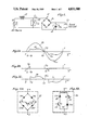
- FIG. 1 is a schematic of one embodiment of the power supply circuit including an inductor and a controlled switch that provides a high power factor.
- FIG. 2A is a graph of one cycle of the source voltage and source current as a function of time.
- FIG. 2B is a graph of the current through the active switch as a function of time.
- FIG. 2C is a graph of the current through the AC terminals of the rectifier as a function of time.
- FIG. 3A shows a circuit implementation of the active switch.
- FIG. 3B shows another implementation of the active switch.
- FIG. 4 is a typical graph of power factor vs. conduction time t 2 -t 1 for different values of inductance.
- FIG. 5 is a typical graph of power factor vs. conduction time t 2 -t 1 for different values of load power.
- FIG. 6 is a graph of the ratio e o /e in vs. switch conduction time t 2 -t 1 for different values of load power.
- FIG. 7A is a block diagram of the control circuit and the control parameters.
- FIG. 7B is a graph illustrating the control parameters and control circuit output signal.
- FIG. 8 is a block diagram of a control circuit with interconnecting elements.
- FIG. 9 is another embodiment of the power supply circuit.
- FIG. 10 is a further embodiment of the power supply circuit.
- FIG. 11 is an additional embodiment of the power supply circuit.
- FIG. 12 is a partial preferred embodiment of the power supply circuit.
- FIG. 13A is a second portion of the power supply circuit connected in FIG. 12.
- FIG. 13B is the last portion of the power supply circuit connected in FIG. 12 and interconnected to FIG. 13A at X.
- FIG. 1 a fundamental circuit diagram of a power supply circuit utilizing the power factor improvement circuit is shown in FIG. 1.
- a linear inductor 12 is connected in series with the alternating current (AC) source 14 and rectifier circuit 16 as shown.
- the output of rectifier 16 is connected to a capacitor 18 for providing a smoothed DC voltage for the load circuit 20.
- an active switching device 22 is connected across the AC terminals of the rectifier 16 between inductor 12 and rectifier 16.
- the switching device 22 is controlled to switch in synchronous relation to the AC input voltage waveform as shown in FIGS. 2A, 2B and 2C.
- the device is switched to a conducting state at time t 1 , and switched off to a non-conducting state at time t 2 .
- the switch 22 is switched on and off once in each half cycle of the AC input voltage waveform.
- the source current i in flows through inductor 12, rectifier 16, filter 18 and load circuit 20 when switch 22 is nonconducting.
- the source current i in flows from AC source through inductor 12 and switch 22 between t 1 and t 2 when switch 22 is conducting.
- the source current i in is shown in FIG. 2A as 24, switch current i s is shown in FIG. 2B as 26, and current i r is shown in FIG. 2C as 28.
- Source current is built up between t 1 and t 2 during the initial part of the AC input waveform when switch 22 is conducting.
- the input current waveform can be controlled to achieve a waveform that is relatively low in harmonic content and having a fundamental frequency component in phase with the AC source voltage waveform e in shown in FIG. 2A as 30. These are necessary criteria for achieving high power factor.
- the power factor is increased to values typically above 0.95.
- FIG. 3A and FIG. 3B show examples of practical implementations of the active switch.
- FIG. 3A shows switch 32 consisting of a bridge rectifier (CR1-CR4) with a transistor switch 34 connected across the DC terminals c and d.
- CR1-CR4 bridge rectifier
- FIG. 3B shows switch 36 consisting of a bridge rectifier (CR1-CR4) with a transistor switch 34 connected across the DC terminals c and d.
- An alernative method would be to fix time t 2 at a defined maximum value and control the turn-on time t 1 . It is essential that the conduction of the switch occurs during the leading or initial part of each half-cycle of the input voltage waveform. For a 60 Hz AC source t 2 -t 1 would be varied by control means over a typical range 0 to 2.5 ms.
- FIG. 4 shows typical curves of power factor vs conduction time t 2 -t 1 for different relative values of inductance L (L 1 , L 2 , L 3 and L 4 ).
- the maximum value of the power factor (PF) will change as shown in FIG. 5.
- the optimum value of inductance is chosen to achieve the highest power factor at rated power P 1 .
- Optimum power factor remains high over relatively wide load ranges as t 2 -t 1 is adjusted to achieve the optimum power factor (PF) for each load condition.
- the DC load voltage increases as conduction time increases for fixed input voltage and load power conditions. As load power is reduced the conduction time must be reduced to maintain a fixed DC voltage across the load. This reduction in conduction time is also necessary to maintain the optimum power factor for reduced load. By maintaining the ratio K at approximately 0.9 the power factor will remain relatively high and constant for changes in AC input voltage, input frequency, and load.
- t 2 -t 1 is controlled according to the relationship defined in FIG. 6.
- t 2 -t 1 is controlled to maintain the DC voltage across the load at the optimum value with respect to the AC input voltage. This is simply done by a control means which compares the DC voltage across the load to a DC voltage proportional to the peak value of the AC input voltage to adjust t 2 -t 1 to maintain the ratio K at a constant value.
- FIG. 7 shows a control block 46 which has two inputs, a low frequency synch signal e s proportional to the AC source and an analog control input signal e t to control t 2 -t 1 .
- the output signal e d drives the synchronous switch to force it into conduction during time t 2 -t 1 .
- Two methods of control are preferred. t 1 can be fixed and t 2 controlled or t 2 can be fixed and t 1 controlled.
- FIG. 8 showing a block diagram of the complete control circuit 49 utilizing filtered DC load voltage e o at 48, AC source voltage 14, a variable DC reference e ref 52 proportional to the AC input voltage 14, a voltage e f 50 proportional to the DC voltage 48 across the load, an error amplifier 54, and synchronized control circuit 46 as defined in FIG. 7.
- the voltage e f at 50 is compared with e ref at 52 by the error amplifier 54.
- the error signal is amplified to provide an analog input e t to the control circuit 46.
- the output signal e d at 56 is a switched output signal with t 2 -t 1 made proportional to the magnitude of the analog input e t .
- e ref will be constant providing a fixed reference input to the error amplifier. If the voltage across the load e o increases e f will increase. The error signal e f -e ref is amplified to provide a corrective input e t to the control circuit 46. t 2 -t 1 is therefore changed to correct e o and force e o to be constant. e o will remain constant for changes in load current and source frequency. Therefore, K will be held constant at its optimum value providing relatively high power factor.
- FIGS. 9, 10 and 11 Alternate construction for the power factor correction circuit are shown in FIGS. 9, 10 and 11. Although the preferred embodiment is as shown in FIG. 1 and FIG. 12, other configurations are possible placing the inductor and switch in the output or DC side of the rectifier 16 as shown in FIGS. 9, 10 and 11.
- FIG. 9 shows switch 22' connected across the output of rectifier 16.
- a rectifier must be inserted between the switch 22 and filter 18 to block current flow from the filter back into the switch 22' when 22' is conducting.
- This circuit adds another rectifier 23 in series with the load circuit reducing the circuit efficiency. Power factor improvement will be achieved as described as set forth above.
- FIG. 10 shows both the inductor 12" and switch 22" connected across the output of rectifier 16. This circuit will have similar performance to that of FIG. 9. This circuit configuration shown in FIG. 10 will provide similar performance to that of FIG. 9 only under the condition that the current in inductor 12" goes to zero prior to the end of each AC cycle as it does in the circuit of FIG. 1.
- FIG. 11 shows a configuration where the switch 22'" utilizes diodes 58 and 60 in combination with two diodes in rectifier 16 to provide performance similar to that described for FIG. 1. This circuit may be preferred over FIG. 1 where a full wave rectifier bridge and single capacitor filter is utilized as shown.
- FIGS. 12, 13A and 13B A preferred embodiment of the invention is shown in FIGS. 12, 13A and 13B.
- An AC input 114 is connected to inductor 112 which is connected between the AC source 114 and bridge rectifier 116. It is common to configure a power supply to operate from either 115 VAC or 230 VAC sources with provision in the power supply to change by appropriate taps as shown. This is done by a rectifier 116, filter 118, and switch arrangement as shown.
- 230 VAC operation the switch A is open and rectifier 116 operates as a conventional full wave bridge.
- For 115 VAC operation switch A is closed and rectifier 116 operates as a voltage doubler circuit.
- the nominal DC output voltage across the load is the same. This allows the use of a high frequency switching power supply load circuit which operates from the same nominal voltage independent of the nominal AC input. Typically the voltage across the load 120 will be approximately 290 VDC with the AC input voltage at 115 VAC or 230 VAC.
- the inductor 112 is tapped to provide an inductance at 230 VAC which is four (4) times the inductance at 115 VAC. This is easily done by providing two identical windings which are connected in parallel for 115 VAC operation and in series for 230 VAC operation. Utilizing this simple tapping arrangement, the power factor control is optimum for both AC input ranges.
- the source current is one half the magnitude at 115 VAC and the inductive impedance for optimum power factor control must be four (4) times that at 115 VAC operation and 37.6 mhy for 230 VAC operation for a power supply rated to supply approximately 1000 watts of load to load circuit 120.
- the active switch 122 is implemented with a simple bridge rectifier 124 and FET switch 126.
- the on-time t 2 -t 1 is controlled by the gate drive circuit and control circuit to be described further.
- a tapped control transformer 128 is used to provide the control power and signals necessary for power factor control.
- the input windings are tapped in a conventional manner to operate from either 115 VAC or 230 VAC source systems.
- the secondary winding voltage is rectified by bridge rectifier 130 to provide a filtered DC voltage E 1 , across capacitor C3 which is proportional to the source voltage. This voltage drives the control circuit and is used as the variable reference for power factor control.
- a zero crossing detector 132 is used to synchronize the switching of switch 122.
- the zero crossing detector senses when the AC voltage crosses zero by the rectifier 134 and resistor divider circuit and provides a reset voltage to a ramp generator circuit 136.
- Capacitor C4 in the ramp generator circuit charges in an approximate linear relationship with time by a fixed supply source of current.
- the reset voltage is provided by the emitter of 138.
- the output of the zero crossing detector goes to a low DC level pulling the base and emitter of 138 to a low DC level. This provides a low impedance discharge of 136 to reset the ramp generator. This occurs at each zero crossing of the AC source voltage.
- a level detector 143 senses the voltage across capacitor 136 and compares it to a variable DC signal derived from the output of the error amplifier 150.
- the output of the level detector is high and provides positive base drive to transistor 140.
- this provides a current in the LED circuit of the opto-coupler 146 providing positive drive to the base of 142 and then 148.
- the emitter of 148 goes positive and provides positive gate drive to 126.
- 126 is in a conducting state immediately at the zero crossing of the AC source and remains conducting until the voltage across 136 becomes more positive then the output of the error amplifier. At this point 140 becomes nonconducting and 126 turns off.
- current flowing in L transfers from the active switch 122 to the rectifier circuit 116.
- the conduction time t 2 -t 1 is a function of the voltage at the output of the error amplifier 150. t 2 -t 1 goes to zero when the error signal goes to zero. t 2 -t 1 increases in time when the error signal increases in a positive direction.
- the voltage e o across the load circuit 120 is compared with a reference DC voltage E 1 which is proportional to the AC source voltage and the difference voltage is amplified by the error amplifier 150 to provide the control input to the level detector. If a disturbance causes e o to increase in magnitude the error amplifier provides a lower DC output signal which reduces the time t 2 -t 1 . A reduction in t 2 -t 1 reduces the output voltage e o to correct for the change in e o .
- the output voltage e o will be held constant for fixed values of E 1 at fixed values for AC input voltage. If the source voltage increases, E 1 will increase, and the output voltage e o will increase proportionally.
- the voltage across the load will track or follow changes in AC input voltage, an important criteria for maintaining the power factor constant for variations in source voltage, frequency, and load.
- This invention can be typically used for the normal power system frequencies at 50 to 60 Hz and may be used at military frequencies at 400 Hz.
- a dynamic current limit circuit is provided to protect 126 under transient conditions.
- Current in 126 is sensed by resistor R 1 and when a threshold level is exceeded Q 2 turns on forcing Q 3 to conduct.
- Positive feedback through R 2 latches the circuit into a conductive state reducing the gate drive to turn the FET switch 126 off.
- the circuit is reset once each half cycle when the drive from 148 goes to zero.
- Transistor Q 4 provides a low impedance turn-off signal when the drive from 148 goes to zero.
Abstract
Description
PF=(P.sub.in /E.sub.RMS I.sub.RMS)
Claims (7)
Priority Applications (1)
| Application Number | Priority Date | Filing Date | Title |
|---|---|---|---|
| US07/111,409 US4831508A (en) | 1987-10-20 | 1987-10-20 | Power supply system having improved input power factor |
Applications Claiming Priority (1)
| Application Number | Priority Date | Filing Date | Title |
|---|---|---|---|
| US07/111,409 US4831508A (en) | 1987-10-20 | 1987-10-20 | Power supply system having improved input power factor |
Publications (1)
| Publication Number | Publication Date |
|---|---|
| US4831508A true US4831508A (en) | 1989-05-16 |
Family
ID=22338374
Family Applications (1)
| Application Number | Title | Priority Date | Filing Date |
|---|---|---|---|
| US07/111,409 Expired - Fee Related US4831508A (en) | 1987-10-20 | 1987-10-20 | Power supply system having improved input power factor |
Country Status (1)
| Country | Link |
|---|---|
| US (1) | US4831508A (en) |
Cited By (77)
| Publication number | Priority date | Publication date | Assignee | Title |
|---|---|---|---|---|
| US4980812A (en) * | 1989-11-09 | 1990-12-25 | Exide Electronics | Uninterrupted power supply system having improved power factor correction circuit |
| US4982148A (en) * | 1989-12-01 | 1991-01-01 | Engelmann Rudolph H | Power factor maintenance system |
| US5012161A (en) * | 1989-01-05 | 1991-04-30 | General Electric Company | Power factor correction circuit |
| US5047912A (en) * | 1990-03-09 | 1991-09-10 | International Rectifier Corporation | Four-terminal unity power factor electronic rectifier |
| US5119285A (en) * | 1991-04-03 | 1992-06-02 | Wayne State University | Solid-state power transformer circuit |
| US5155430A (en) * | 1989-12-01 | 1992-10-13 | Zdzislaw Gulczynski | Switching power supply with constant or sinusoidal input current and with fixed or variable output voltage |
| WO1994000908A1 (en) * | 1992-06-23 | 1994-01-06 | Delta Coventry Corporation | Power factor correction circuit for ac to dc power supply |
| EP0580237A1 (en) * | 1992-07-20 | 1994-01-26 | N.V. Nederlandsche Apparatenfabriek NEDAP | Power factor correction circuit |
| DE4232829A1 (en) * | 1992-09-30 | 1994-03-31 | Siemens Nixdorf Inf Syst | Circuit arrangement for generating a DC voltage |
| US5345164A (en) * | 1993-04-27 | 1994-09-06 | Metcal, Inc. | Power factor corrected DC power supply |
| US5383109A (en) * | 1993-12-10 | 1995-01-17 | University Of Colorado | High power factor boost rectifier apparatus |
| US5479336A (en) * | 1992-08-06 | 1995-12-26 | Mitsubishi Denki Kabushiki Kaisha | DC power-supply unit |
| US5502630A (en) * | 1994-07-19 | 1996-03-26 | Transistor Devices, Inc. | Power factor corrected rectification |
| EP0732797A1 (en) | 1995-03-16 | 1996-09-18 | FRANKLIN ELECTRIC Co., Inc. | Power factor correction |
| US5594632A (en) * | 1994-10-03 | 1997-01-14 | Delco Electronics Corporation | Power converter with harmonic neutralization |
| EP0692863A3 (en) * | 1994-07-13 | 1997-05-21 | Vlt Corp | AC to DC boost switching power conversion |
| JPH11164562A (en) * | 1997-09-24 | 1999-06-18 | Toshiba Corp | Power converter and air conditioner using the same |
| US5920473A (en) * | 1998-03-09 | 1999-07-06 | Magnetic Technology, Inc. | Dc-to-Dc power converter with integrated magnetic power transformer |
| DE19826895A1 (en) * | 1998-06-17 | 1999-12-23 | Eckhardt Gruensch | Voltage regulation method for regulated voltage supply for sensitive electrical load e.g. audio amplifier |
| US6057674A (en) * | 1993-11-22 | 2000-05-02 | Ultrawatt Integrated Systems, Inc. | Energy saving power control system |
| US6104172A (en) * | 1997-07-01 | 2000-08-15 | Power-One | Power factor corrector |
| US6172489B1 (en) | 1999-12-28 | 2001-01-09 | Ultrawatt.Com Inc. | Voltage control system and method |
| US6282109B1 (en) * | 2000-04-28 | 2001-08-28 | Simon Fraidlin | Controller for a non-isolated power factor corrector and method of regulating the power factor corrector |
| EP1022844A3 (en) * | 1999-01-19 | 2002-04-17 | Matsushita Electric Industrial Co., Ltd. | Power supply device and air conditioner using the same |
| US6377481B1 (en) | 1999-06-30 | 2002-04-23 | Peco Ii, Inc. | Power supply including diode recovery current suppression circuit |
| EP1229633A1 (en) * | 2001-02-02 | 2002-08-07 | ADI Corporation | Switching power factor correction apparatus and method thereof |
| US6608770B2 (en) * | 2001-08-31 | 2003-08-19 | Vlt Corporation | Passive control of harmonic current drawn from an AC input by rectification circuitry |
| US6611169B2 (en) | 2001-10-01 | 2003-08-26 | Gibson Guitar Corp. | Power supply regulation and protection circuit for audio power amplifier |
| US6653822B2 (en) * | 2001-02-22 | 2003-11-25 | Koninklijke Philips Electronics N.V. | Circuit for converting AC voltage into DC voltage |
| US6661678B2 (en) | 1993-03-29 | 2003-12-09 | Powerware Corporation | Power factor corrected UPS with improved connection of battery to neutral and methods of operation thereof |
| US6697265B2 (en) * | 2001-05-23 | 2004-02-24 | Advanced Energy Industries, Inc. | Wide range DC power supply utilizing voltage doubling output capacitors and inductive choke to extend full power load impedance range |
| US20040190313A1 (en) * | 2003-03-25 | 2004-09-30 | Switching Power, Inc. | Switched linear inductor circuit for switched power supply |
| DE19828584B4 (en) * | 1997-06-27 | 2005-07-28 | Kabushiki Kaisha Toshiba, Kawasaki | DC power supply system |
| US20050162129A1 (en) * | 2004-01-23 | 2005-07-28 | Srdan Mutabdzija | Method and apparatus for monitoring energy storage devices |
| US20050162836A1 (en) * | 2004-01-23 | 2005-07-28 | James Briggs | Modular UPS |
| US20050162019A1 (en) * | 2004-01-23 | 2005-07-28 | Masciarelli Francis J. | Methods and apparatus for providing uninterruptible power |
| WO2005107054A1 (en) * | 2004-04-29 | 2005-11-10 | Koninklijke Philips Electronics N.V. | Boost converter |
| US20060044846A1 (en) * | 2004-08-31 | 2006-03-02 | American Power Conversion Corporation | Method and apparatus for providing uninterruptible power |
| US20060043793A1 (en) * | 2004-08-31 | 2006-03-02 | American Power Conversion Corporation | Method and apparatus for providing uninterruptible power |
| US20060043797A1 (en) * | 2004-08-31 | 2006-03-02 | American Power Conversion Corporation | Method and apparatus for providing uninterruptible power |
| US20060238941A1 (en) * | 2005-04-21 | 2006-10-26 | American Power Conversion Corporation | Method and apparatus for providing uninterruptible power |
| US20080041076A1 (en) * | 2006-08-15 | 2008-02-21 | American Power Conversion Corporation | Method and apparatus for cooling |
| US20080061628A1 (en) * | 2006-09-08 | 2008-03-13 | American Power Conversion Corporation | Method and apparatus for providing uninterruptible power |
| WO2008044120A2 (en) * | 2006-10-11 | 2008-04-17 | O.C.E.M. S.P.A. | A device for supplying power to led diodes |
| US20080142068A1 (en) * | 2006-12-18 | 2008-06-19 | American Power Conversion Corporation | Direct Thermoelectric chiller assembly |
| EP1944856A1 (en) * | 2007-01-15 | 2008-07-16 | O.Y.L. Research & Development Centre Sdn Bhd | A power factor correction circuit |
| US20080180908A1 (en) * | 2007-01-23 | 2008-07-31 | Peter Wexler | In-row air containment and cooling system and method |
| US20080245083A1 (en) * | 2006-08-15 | 2008-10-09 | American Power Conversion Corporation | Method and apparatus for cooling |
| US7456518B2 (en) | 2004-08-31 | 2008-11-25 | American Power Conversion Corporation | Method and apparatus for providing uninterruptible power |
| US20090237963A1 (en) * | 2008-03-24 | 2009-09-24 | Pyboyina Prasad | Ups frequency converter and line conditioner |
| US20090257259A1 (en) * | 2008-04-15 | 2009-10-15 | Powermat Ltd. | Bridge synchronous rectifier |
| US20100057263A1 (en) * | 2006-08-15 | 2010-03-04 | Ozan Tutunoglu | Method and apparatus for cooling |
| US20100170663A1 (en) * | 2006-12-18 | 2010-07-08 | American Power Conversion Corporation | Modular ice storage for uninterruptible chilled water |
| US20100188066A1 (en) * | 2009-01-27 | 2010-07-29 | American Power Conversion Corporation | System and method for limiting losses in an uninterruptible power supply |
| US20100211669A1 (en) * | 2009-02-13 | 2010-08-19 | American Power Conversion Corporation | Data center control |
| US20100315849A1 (en) * | 2009-06-16 | 2010-12-16 | American Power Conversion Corporation | Power supply control |
| WO2012004927A1 (en) * | 2010-07-08 | 2012-01-12 | パナソニック株式会社 | Rectifier circuit device |
| US8116105B2 (en) | 2008-02-07 | 2012-02-14 | American Power Conversion Corporation | Systems and methods for uninterruptible power supply control |
| US8259475B2 (en) * | 2010-11-30 | 2012-09-04 | Samsung Electro-Mechanics Co. Ltd. | Power supply circuit having AC power discharging functions |
| WO2013088652A1 (en) * | 2011-12-14 | 2013-06-20 | パナソニック株式会社 | Dc power supply device |
| US8503201B2 (en) | 2009-12-03 | 2013-08-06 | Schneider Electric It Corporation | Transient clamping circuitry for voltage converter |
| US8552589B2 (en) | 2010-05-14 | 2013-10-08 | Schneider Electric It Corporation | Digital control method for operating the UPS systems in parallel |
| US8698354B2 (en) | 2010-11-05 | 2014-04-15 | Schneider Electric It Corporation | System and method for bidirectional DC-AC power conversion |
| US8803361B2 (en) | 2011-01-19 | 2014-08-12 | Schneider Electric It Corporation | Apparatus and method for providing uninterruptible power |
| US8878389B2 (en) | 2011-01-11 | 2014-11-04 | Schneider Electric It Corporation | Method and apparatus for providing uninterruptible power |
| US8884464B2 (en) | 2011-08-29 | 2014-11-11 | Schneider Electric It Corporation | Twin boost converter with integrated charger for UPS system |
| US20150326138A1 (en) * | 2014-05-09 | 2015-11-12 | Andreas Stihl Ag & Co. Kg | Capacitor power supply unit for small electrical loads with a high current requirement |
| US20170302150A1 (en) * | 2014-09-30 | 2017-10-19 | Mitsubishi Electric Corporation | Power converting apparatus |
| US9830410B2 (en) | 2011-12-22 | 2017-11-28 | Schneider Electric It Corporation | System and method for prediction of temperature values in an electronics system |
| US9952103B2 (en) | 2011-12-22 | 2018-04-24 | Schneider Electric It Corporation | Analysis of effect of transient events on temperature in a data center |
| WO2018124930A1 (en) * | 2016-12-30 | 2018-07-05 | Владимир Евгеньевич РЫЖАКОВ | Current stabilization device with active power factor corrector |
| JP2019080408A (en) * | 2017-10-23 | 2019-05-23 | 日立ジョンソンコントロールズ空調株式会社 | Dc power supply and air conditioner |
| WO2019125206A1 (en) * | 2017-12-22 | 2019-06-27 | Аркадий Анатольевич СТЕПАНОВ | Economical closed-loop inductive inverter |
| US10459464B2 (en) | 2012-09-03 | 2019-10-29 | Schneider Electric It Corporation | Method and apparatus for controlling distribution of power |
| US11076507B2 (en) | 2007-05-15 | 2021-07-27 | Schneider Electric It Corporation | Methods and systems for managing facility power and cooling |
| US11387688B2 (en) | 2008-07-02 | 2022-07-12 | Powermat Technologies, Ltd. | System and method for coded communication signals regulating inductive power transmissions |
| US11837399B2 (en) | 2008-03-17 | 2023-12-05 | Powermat Technologies, Ltd. | Transmission-guard system and method for an inductive power supply |
Citations (6)
| Publication number | Priority date | Publication date | Assignee | Title |
|---|---|---|---|---|
| US4074344A (en) * | 1975-09-22 | 1978-02-14 | Gte Sylvania Incorporated | High power factor ac to dc converter circuit |
| JPS5317931A (en) * | 1976-07-31 | 1978-02-18 | Hitachi Ltd | Electric current source circuit |
| US4222096A (en) * | 1978-12-05 | 1980-09-09 | Lutron Electronics Co., Inc. | D-C Power supply circuit with high power factor |
| US4340931A (en) * | 1979-11-30 | 1982-07-20 | Hitachi, Ltd. | Power supply system |
| US4369490A (en) * | 1979-12-14 | 1983-01-18 | Patent-Treuhand-Gesellschaft Fur Elektrische Gluhlampen | Low-ripple power rectifier system |
| US4683529A (en) * | 1986-11-12 | 1987-07-28 | Zytec Corporation | Switching power supply with automatic power factor correction |
-
1987
- 1987-10-20 US US07/111,409 patent/US4831508A/en not_active Expired - Fee Related
Patent Citations (6)
| Publication number | Priority date | Publication date | Assignee | Title |
|---|---|---|---|---|
| US4074344A (en) * | 1975-09-22 | 1978-02-14 | Gte Sylvania Incorporated | High power factor ac to dc converter circuit |
| JPS5317931A (en) * | 1976-07-31 | 1978-02-18 | Hitachi Ltd | Electric current source circuit |
| US4222096A (en) * | 1978-12-05 | 1980-09-09 | Lutron Electronics Co., Inc. | D-C Power supply circuit with high power factor |
| US4340931A (en) * | 1979-11-30 | 1982-07-20 | Hitachi, Ltd. | Power supply system |
| US4369490A (en) * | 1979-12-14 | 1983-01-18 | Patent-Treuhand-Gesellschaft Fur Elektrische Gluhlampen | Low-ripple power rectifier system |
| US4683529A (en) * | 1986-11-12 | 1987-07-28 | Zytec Corporation | Switching power supply with automatic power factor correction |
Cited By (135)
| Publication number | Priority date | Publication date | Assignee | Title |
|---|---|---|---|---|
| US5012161A (en) * | 1989-01-05 | 1991-04-30 | General Electric Company | Power factor correction circuit |
| WO1991007808A1 (en) * | 1989-11-09 | 1991-05-30 | Exide Electronics International Corporation | An uninterrupted power supply system having improved power factor correction circuit |
| US4980812A (en) * | 1989-11-09 | 1990-12-25 | Exide Electronics | Uninterrupted power supply system having improved power factor correction circuit |
| US4982148A (en) * | 1989-12-01 | 1991-01-01 | Engelmann Rudolph H | Power factor maintenance system |
| US5155430A (en) * | 1989-12-01 | 1992-10-13 | Zdzislaw Gulczynski | Switching power supply with constant or sinusoidal input current and with fixed or variable output voltage |
| US5047912A (en) * | 1990-03-09 | 1991-09-10 | International Rectifier Corporation | Four-terminal unity power factor electronic rectifier |
| US5119285A (en) * | 1991-04-03 | 1992-06-02 | Wayne State University | Solid-state power transformer circuit |
| US5416687A (en) * | 1992-06-23 | 1995-05-16 | Delta Coventry Corporation | Power factor correction circuit for AC to DC power supply |
| WO1994000908A1 (en) * | 1992-06-23 | 1994-01-06 | Delta Coventry Corporation | Power factor correction circuit for ac to dc power supply |
| EP0580237A1 (en) * | 1992-07-20 | 1994-01-26 | N.V. Nederlandsche Apparatenfabriek NEDAP | Power factor correction circuit |
| US5479336A (en) * | 1992-08-06 | 1995-12-26 | Mitsubishi Denki Kabushiki Kaisha | DC power-supply unit |
| DE4232829A1 (en) * | 1992-09-30 | 1994-03-31 | Siemens Nixdorf Inf Syst | Circuit arrangement for generating a DC voltage |
| US7082040B2 (en) | 1993-03-29 | 2006-07-25 | Eaton Power Quality Corporation | Power factor corrected UPS with improved connection of battery to neutral |
| US20040213022A1 (en) * | 1993-03-29 | 2004-10-28 | Raddi William J. | Power factor corrected UPS with improved connection of battery to neutral |
| US6944035B2 (en) | 1993-03-29 | 2005-09-13 | Eaton Power Quality Corporation | Power factor corrected UPS with improved connection of battery to neutral |
| US6661678B2 (en) | 1993-03-29 | 2003-12-09 | Powerware Corporation | Power factor corrected UPS with improved connection of battery to neutral and methods of operation thereof |
| US5345164A (en) * | 1993-04-27 | 1994-09-06 | Metcal, Inc. | Power factor corrected DC power supply |
| US6191563B1 (en) | 1993-11-22 | 2001-02-20 | Ultrawatt.Com | Energy saving power control system |
| US6057674A (en) * | 1993-11-22 | 2000-05-02 | Ultrawatt Integrated Systems, Inc. | Energy saving power control system |
| US5383109A (en) * | 1993-12-10 | 1995-01-17 | University Of Colorado | High power factor boost rectifier apparatus |
| EP0692863A3 (en) * | 1994-07-13 | 1997-05-21 | Vlt Corp | AC to DC boost switching power conversion |
| US5726872A (en) * | 1994-07-13 | 1998-03-10 | Vlt Corporation | AC to DC boost power converters |
| US5502630A (en) * | 1994-07-19 | 1996-03-26 | Transistor Devices, Inc. | Power factor corrected rectification |
| US5594632A (en) * | 1994-10-03 | 1997-01-14 | Delco Electronics Corporation | Power converter with harmonic neutralization |
| EP0732797A1 (en) | 1995-03-16 | 1996-09-18 | FRANKLIN ELECTRIC Co., Inc. | Power factor correction |
| DE19828584B4 (en) * | 1997-06-27 | 2005-07-28 | Kabushiki Kaisha Toshiba, Kawasaki | DC power supply system |
| US6104172A (en) * | 1997-07-01 | 2000-08-15 | Power-One | Power factor corrector |
| JPH11164562A (en) * | 1997-09-24 | 1999-06-18 | Toshiba Corp | Power converter and air conditioner using the same |
| US5920473A (en) * | 1998-03-09 | 1999-07-06 | Magnetic Technology, Inc. | Dc-to-Dc power converter with integrated magnetic power transformer |
| DE19826895A1 (en) * | 1998-06-17 | 1999-12-23 | Eckhardt Gruensch | Voltage regulation method for regulated voltage supply for sensitive electrical load e.g. audio amplifier |
| EP1022844A3 (en) * | 1999-01-19 | 2002-04-17 | Matsushita Electric Industrial Co., Ltd. | Power supply device and air conditioner using the same |
| USRE39060E1 (en) | 1999-01-19 | 2006-04-11 | Matsushita Electric Industrial Co., Ltd. | Power supply device and air conditioner using the same |
| US6377481B1 (en) | 1999-06-30 | 2002-04-23 | Peco Ii, Inc. | Power supply including diode recovery current suppression circuit |
| US6172489B1 (en) | 1999-12-28 | 2001-01-09 | Ultrawatt.Com Inc. | Voltage control system and method |
| US6282109B1 (en) * | 2000-04-28 | 2001-08-28 | Simon Fraidlin | Controller for a non-isolated power factor corrector and method of regulating the power factor corrector |
| EP1229633A1 (en) * | 2001-02-02 | 2002-08-07 | ADI Corporation | Switching power factor correction apparatus and method thereof |
| US6653822B2 (en) * | 2001-02-22 | 2003-11-25 | Koninklijke Philips Electronics N.V. | Circuit for converting AC voltage into DC voltage |
| US6697265B2 (en) * | 2001-05-23 | 2004-02-24 | Advanced Energy Industries, Inc. | Wide range DC power supply utilizing voltage doubling output capacitors and inductive choke to extend full power load impedance range |
| US6608770B2 (en) * | 2001-08-31 | 2003-08-19 | Vlt Corporation | Passive control of harmonic current drawn from an AC input by rectification circuitry |
| US6611169B2 (en) | 2001-10-01 | 2003-08-26 | Gibson Guitar Corp. | Power supply regulation and protection circuit for audio power amplifier |
| US6853564B2 (en) | 2003-03-25 | 2005-02-08 | Switching Power, Inc. | Switched linear inductor circuit for switched power supply |
| US20040190313A1 (en) * | 2003-03-25 | 2004-09-30 | Switching Power, Inc. | Switched linear inductor circuit for switched power supply |
| US7612472B2 (en) | 2004-01-23 | 2009-11-03 | American Power Conversion Corporation | Method and apparatus for monitoring energy storage devices |
| US8162417B2 (en) | 2004-01-23 | 2012-04-24 | American Power Conversion Corporation | Modular UPS |
| US20050162129A1 (en) * | 2004-01-23 | 2005-07-28 | Srdan Mutabdzija | Method and apparatus for monitoring energy storage devices |
| US7911088B2 (en) | 2004-01-23 | 2011-03-22 | American Power Conversion Corporation | Method and apparatus for monitoring energy storage devices |
| US20100201194A1 (en) * | 2004-01-23 | 2010-08-12 | American Power Conversion Corporation | Methods and apparatus for providing uninterruptible power |
| US20050162019A1 (en) * | 2004-01-23 | 2005-07-28 | Masciarelli Francis J. | Methods and apparatus for providing uninterruptible power |
| US20050162836A1 (en) * | 2004-01-23 | 2005-07-28 | James Briggs | Modular UPS |
| US8604640B2 (en) | 2004-01-23 | 2013-12-10 | Schneider Electric It Corporation | Methods and apparatus for providing uninterruptible power |
| US20080157601A1 (en) * | 2004-01-23 | 2008-07-03 | American Power Conversion Corporation | Methods and apparatus for providing uninterruptible power |
| US7446433B2 (en) | 2004-01-23 | 2008-11-04 | American Power Conversion Corporation | Methods and apparatus for providing uninterruptible power |
| US20100049457A1 (en) * | 2004-01-23 | 2010-02-25 | American Power Conversion Corporation | Method and apparatus for monitoring energy storage devices |
| US7615890B2 (en) | 2004-01-23 | 2009-11-10 | American Power Conversion Corporation | Methods and apparatus for providing uninterruptible power |
| US8854824B2 (en) | 2004-01-23 | 2014-10-07 | Schneider Electric It Corporation | Modular UPS |
| US7379305B2 (en) | 2004-01-23 | 2008-05-27 | American Power Conversion Corporation | Modular UPS |
| US20080278889A1 (en) * | 2004-01-23 | 2008-11-13 | American Power Conversion Corporation | Modular ups |
| US8148846B2 (en) | 2004-01-23 | 2012-04-03 | American Power Conversion Corporation | Methods and apparatus for providing uninterruptible power |
| WO2005107054A1 (en) * | 2004-04-29 | 2005-11-10 | Koninklijke Philips Electronics N.V. | Boost converter |
| US20070211498A1 (en) * | 2004-04-29 | 2007-09-13 | Koninklijke Philips Electronics, N.V. | Boost converter |
| US7939968B2 (en) | 2004-08-31 | 2011-05-10 | American Power Conversion Corporation | Method and apparatus for providing uninterruptible power |
| US20060044846A1 (en) * | 2004-08-31 | 2006-03-02 | American Power Conversion Corporation | Method and apparatus for providing uninterruptible power |
| US7855472B2 (en) | 2004-08-31 | 2010-12-21 | American Power Conversion Corporation | Method and apparatus for providing uninterruptible power |
| US7456518B2 (en) | 2004-08-31 | 2008-11-25 | American Power Conversion Corporation | Method and apparatus for providing uninterruptible power |
| US8053927B2 (en) | 2004-08-31 | 2011-11-08 | American Power Conversion Corporation | Method and apparatus for providing uninterruptible power |
| US20100225170A1 (en) * | 2004-08-31 | 2010-09-09 | American Power Conversion Corporation | Method and apparatus for providing uninterruptible power |
| US20060043793A1 (en) * | 2004-08-31 | 2006-03-02 | American Power Conversion Corporation | Method and apparatus for providing uninterruptible power |
| US20110227415A1 (en) * | 2004-08-31 | 2011-09-22 | American Power Conversion Corporation | Method and apparatus for providing uninterruptible power |
| US20060043797A1 (en) * | 2004-08-31 | 2006-03-02 | American Power Conversion Corporation | Method and apparatus for providing uninterruptible power |
| US7274112B2 (en) | 2004-08-31 | 2007-09-25 | American Power Conversion Corporation | Method and apparatus for providing uninterruptible power |
| US7737580B2 (en) | 2004-08-31 | 2010-06-15 | American Power Conversion Corporation | Method and apparatus for providing uninterruptible power |
| US7402921B2 (en) | 2005-04-21 | 2008-07-22 | American Power Conversion Corporation | Method and apparatus for providing uninterruptible power |
| US20060238941A1 (en) * | 2005-04-21 | 2006-10-26 | American Power Conversion Corporation | Method and apparatus for providing uninterruptible power |
| US9568206B2 (en) | 2006-08-15 | 2017-02-14 | Schneider Electric It Corporation | Method and apparatus for cooling |
| US20100057263A1 (en) * | 2006-08-15 | 2010-03-04 | Ozan Tutunoglu | Method and apparatus for cooling |
| US20080041076A1 (en) * | 2006-08-15 | 2008-02-21 | American Power Conversion Corporation | Method and apparatus for cooling |
| US9115916B2 (en) | 2006-08-15 | 2015-08-25 | Schneider Electric It Corporation | Method of operating a cooling system having one or more cooling units |
| US8322155B2 (en) | 2006-08-15 | 2012-12-04 | American Power Conversion Corporation | Method and apparatus for cooling |
| US8327656B2 (en) | 2006-08-15 | 2012-12-11 | American Power Conversion Corporation | Method and apparatus for cooling |
| US20080245083A1 (en) * | 2006-08-15 | 2008-10-09 | American Power Conversion Corporation | Method and apparatus for cooling |
| US7705489B2 (en) | 2006-09-08 | 2010-04-27 | American Power Conversion Corporation | Method and apparatus for providing uninterruptible power |
| US20080061628A1 (en) * | 2006-09-08 | 2008-03-13 | American Power Conversion Corporation | Method and apparatus for providing uninterruptible power |
| US8143744B2 (en) | 2006-09-08 | 2012-03-27 | American Power Conversion Corporation | Method and apparatus for providing uninterruptible power |
| US20100295374A1 (en) * | 2006-09-08 | 2010-11-25 | American Power Conversion Corporation | Method and apparatus for providing uninterruptible power |
| WO2008044120A3 (en) * | 2006-10-11 | 2008-06-12 | Ocem Spa | A device for supplying power to led diodes |
| US8072154B2 (en) | 2006-10-11 | 2011-12-06 | O.C.E.M. S.P.A. | Device for supplying power to LED diodes |
| US20100102737A1 (en) * | 2006-10-11 | 2010-04-29 | O.C.E.M. S.P.A. | Device For Supplying Power To LED Diodes |
| WO2008044120A2 (en) * | 2006-10-11 | 2008-04-17 | O.C.E.M. S.P.A. | A device for supplying power to led diodes |
| US9080802B2 (en) | 2006-12-18 | 2015-07-14 | Schneider Electric It Corporation | Modular ice storage for uninterruptible chilled water |
| US8424336B2 (en) | 2006-12-18 | 2013-04-23 | Schneider Electric It Corporation | Modular ice storage for uninterruptible chilled water |
| US20100170663A1 (en) * | 2006-12-18 | 2010-07-08 | American Power Conversion Corporation | Modular ice storage for uninterruptible chilled water |
| US20080142068A1 (en) * | 2006-12-18 | 2008-06-19 | American Power Conversion Corporation | Direct Thermoelectric chiller assembly |
| US20080285318A1 (en) * | 2007-01-15 | 2008-11-20 | Oyl Research And Development Centre Sdn. Bhd. | Power Factor Correction Circuit |
| US8164930B2 (en) | 2007-01-15 | 2012-04-24 | Oyl Research And Development Centre Sdn. Bhd. | Power factor correction circuit |
| EP1944856A1 (en) * | 2007-01-15 | 2008-07-16 | O.Y.L. Research & Development Centre Sdn Bhd | A power factor correction circuit |
| KR101455390B1 (en) * | 2007-01-15 | 2014-10-27 | 오와이엘 리서치 앤드 디벨럽먼트 센터 에스디엔 비에치디 | A power factor correction circuit |
| US20080180908A1 (en) * | 2007-01-23 | 2008-07-31 | Peter Wexler | In-row air containment and cooling system and method |
| US8425287B2 (en) | 2007-01-23 | 2013-04-23 | Schneider Electric It Corporation | In-row air containment and cooling system and method |
| US11076507B2 (en) | 2007-05-15 | 2021-07-27 | Schneider Electric It Corporation | Methods and systems for managing facility power and cooling |
| US11503744B2 (en) | 2007-05-15 | 2022-11-15 | Schneider Electric It Corporation | Methods and systems for managing facility power and cooling |
| US8116105B2 (en) | 2008-02-07 | 2012-02-14 | American Power Conversion Corporation | Systems and methods for uninterruptible power supply control |
| US11837399B2 (en) | 2008-03-17 | 2023-12-05 | Powermat Technologies, Ltd. | Transmission-guard system and method for an inductive power supply |
| US20090237963A1 (en) * | 2008-03-24 | 2009-09-24 | Pyboyina Prasad | Ups frequency converter and line conditioner |
| US7881079B2 (en) | 2008-03-24 | 2011-02-01 | American Power Conversion Corporation | UPS frequency converter and line conditioner |
| US8320143B2 (en) * | 2008-04-15 | 2012-11-27 | Powermat Technologies, Ltd. | Bridge synchronous rectifier |
| US20090257259A1 (en) * | 2008-04-15 | 2009-10-15 | Powermat Ltd. | Bridge synchronous rectifier |
| US11387688B2 (en) | 2008-07-02 | 2022-07-12 | Powermat Technologies, Ltd. | System and method for coded communication signals regulating inductive power transmissions |
| US8450876B2 (en) | 2009-01-27 | 2013-05-28 | Schneider Electric It Corporation | System and method for limiting losses in an uninterruptible power supply |
| US20100188066A1 (en) * | 2009-01-27 | 2010-07-29 | American Power Conversion Corporation | System and method for limiting losses in an uninterruptible power supply |
| US8212402B2 (en) | 2009-01-27 | 2012-07-03 | American Power Conversion Corporation | System and method for limiting losses in an uninterruptible power supply |
| US9519517B2 (en) | 2009-02-13 | 2016-12-13 | Schneider Electtic It Corporation | Data center control |
| US20100211669A1 (en) * | 2009-02-13 | 2010-08-19 | American Power Conversion Corporation | Data center control |
| US20100315849A1 (en) * | 2009-06-16 | 2010-12-16 | American Power Conversion Corporation | Power supply control |
| US8228046B2 (en) | 2009-06-16 | 2012-07-24 | American Power Conversion Corporation | Apparatus and method for operating an uninterruptible power supply |
| US8503201B2 (en) | 2009-12-03 | 2013-08-06 | Schneider Electric It Corporation | Transient clamping circuitry for voltage converter |
| US8552589B2 (en) | 2010-05-14 | 2013-10-08 | Schneider Electric It Corporation | Digital control method for operating the UPS systems in parallel |
| US9373979B2 (en) | 2010-05-14 | 2016-06-21 | Schneider Electric It Corporation | Digital control method for operating UPS systems in parallel |
| WO2012004927A1 (en) * | 2010-07-08 | 2012-01-12 | パナソニック株式会社 | Rectifier circuit device |
| US8698354B2 (en) | 2010-11-05 | 2014-04-15 | Schneider Electric It Corporation | System and method for bidirectional DC-AC power conversion |
| US8259475B2 (en) * | 2010-11-30 | 2012-09-04 | Samsung Electro-Mechanics Co. Ltd. | Power supply circuit having AC power discharging functions |
| US8878389B2 (en) | 2011-01-11 | 2014-11-04 | Schneider Electric It Corporation | Method and apparatus for providing uninterruptible power |
| US8803361B2 (en) | 2011-01-19 | 2014-08-12 | Schneider Electric It Corporation | Apparatus and method for providing uninterruptible power |
| US8884464B2 (en) | 2011-08-29 | 2014-11-11 | Schneider Electric It Corporation | Twin boost converter with integrated charger for UPS system |
| WO2013088652A1 (en) * | 2011-12-14 | 2013-06-20 | パナソニック株式会社 | Dc power supply device |
| US9952103B2 (en) | 2011-12-22 | 2018-04-24 | Schneider Electric It Corporation | Analysis of effect of transient events on temperature in a data center |
| US9830410B2 (en) | 2011-12-22 | 2017-11-28 | Schneider Electric It Corporation | System and method for prediction of temperature values in an electronics system |
| US10459464B2 (en) | 2012-09-03 | 2019-10-29 | Schneider Electric It Corporation | Method and apparatus for controlling distribution of power |
| US9525360B2 (en) * | 2014-05-09 | 2016-12-20 | Andreas Stihl Ag & Co. Kg | Capacitor power supply unit for small electrical loads with a high current requirement |
| US20150326138A1 (en) * | 2014-05-09 | 2015-11-12 | Andreas Stihl Ag & Co. Kg | Capacitor power supply unit for small electrical loads with a high current requirement |
| FR3020904A1 (en) * | 2014-05-09 | 2015-11-13 | Stihl Ag & Co Kg Andreas | CAPACITOR POWER SUPPLY BLOCK FOR SMALL ELECTRIC CONSUMERS NEEDED IN HIGH CURRENT |
| US9941780B2 (en) * | 2014-09-30 | 2018-04-10 | Mitsubishi Electric Corporation | Power conversion device with correction of reactor inductance based on detected current |
| US20170302150A1 (en) * | 2014-09-30 | 2017-10-19 | Mitsubishi Electric Corporation | Power converting apparatus |
| WO2018124930A1 (en) * | 2016-12-30 | 2018-07-05 | Владимир Евгеньевич РЫЖАКОВ | Current stabilization device with active power factor corrector |
| JP2019080408A (en) * | 2017-10-23 | 2019-05-23 | 日立ジョンソンコントロールズ空調株式会社 | Dc power supply and air conditioner |
| WO2019125206A1 (en) * | 2017-12-22 | 2019-06-27 | Аркадий Анатольевич СТЕПАНОВ | Economical closed-loop inductive inverter |
Similar Documents
| Publication | Publication Date | Title |
|---|---|---|
| US4831508A (en) | Power supply system having improved input power factor | |
| US3913002A (en) | Power circuits for obtaining a high power factor electronically | |
| US6069798A (en) | Asymmetrical power converter and method of operation thereof | |
| EP0678972B1 (en) | A control circuit for an inductive load | |
| US5510974A (en) | High frequency push-pull converter with input power factor correction | |
| US5434767A (en) | Power converter possessing zero-voltage switching and output isolation | |
| US5508904A (en) | Switching regulator having superimposing chopping-wave voltage forming circuit | |
| US5216585A (en) | Switching power source device | |
| US6441590B1 (en) | Two stage architecture for a monitor power supply | |
| EP1776752A2 (en) | Low switching frequency power factor correction circuit | |
| EP0503862A2 (en) | Class E fixed frequency converter | |
| JPH04331460A (en) | Power converter | |
| US5835368A (en) | Power-factor improvement converter | |
| JPS5989576A (en) | High frequency series resonance dc/dc converter | |
| US5155430A (en) | Switching power supply with constant or sinusoidal input current and with fixed or variable output voltage | |
| US4791545A (en) | Zero-crossover SCR power supply regulator | |
| US7317624B2 (en) | Power factor correction method and apparatus and power supply using the same | |
| US5712780A (en) | Unity power factor converter for high quality power supply with magnetically coupled compensation | |
| Bourgeois | Circuits for power factor correction with regards to mains filtering | |
| US4523266A (en) | AC to DC conversion system with current spreading circuit | |
| KR100867452B1 (en) | Low switching frequency power factor correction circuit | |
| JP2512040B2 (en) | Power supply | |
| JP2677738B2 (en) | Switching regulator | |
| JP3027284B2 (en) | Switching power supply | |
| JPS63228967A (en) | Resonance type switching power source |
Legal Events
| Date | Code | Title | Description |
|---|---|---|---|
| AS | Assignment |
Owner name: COMPUTER PRODUCTS, INC., 2900 GATEWAY DRIVE, POMPA Free format text: ASSIGNMENT OF ASSIGNORS INTEREST.;ASSIGNOR:HUNTER, PATRICK L.;REEL/FRAME:004780/0237 Effective date: 19871029 Owner name: COMPUTER PRODUCTS, INC.,FLORIDA Free format text: ASSIGNMENT OF ASSIGNORS INTEREST;ASSIGNOR:HUNTER, PATRICK L.;REEL/FRAME:004780/0237 Effective date: 19871029 |
|
| FPAY | Fee payment |
Year of fee payment: 4 |
|
| SULP | Surcharge for late payment | ||
| FPAY | Fee payment |
Year of fee payment: 8 |
|
| REMI | Maintenance fee reminder mailed | ||
| LAPS | Lapse for failure to pay maintenance fees | ||
| FP | Lapsed due to failure to pay maintenance fee |
Effective date: 20010516 |
|
| AS | Assignment |
Owner name: BANK OF AMERICA, N.A., CALIFORNIA Free format text: SECURITY AGREEMENT;ASSIGNORS:ARTESYN TECHNOLOGIES, INC., ARTESYN NORTH AMERICA, INC.;ARTESYN CAYMAN LP, ARTESYN DELAWARE LLC;ARTESYN TECHNOLOGIES COMMUNICATION PRODUCTS, INC.;AND OTHERS;REEL/FRAME:012551/0310 Effective date: 20020115 |
|
| AS | Assignment |
Owner name: ARTESYN TECHNOLOGIES, INC., FLORIDA Free format text: CHANGE OF NAME;ASSIGNOR:COMPUTER PRODUCTS, INC.;REEL/FRAME:013879/0484 Effective date: 19980506 |
|
| AS | Assignment |
Owner name: ARTESYN CAYMAN LP, FLORIDA Free format text: RELEASE OF SECURITY INTEREST;ASSIGNOR:BANK OF AMERICA, N.A., AS AGENT;REEL/FRAME:013933/0579 Effective date: 20030326 Owner name: ARTESYN COMMUNICATION PRODUCTS, INC., WISCONSIN Free format text: RELEASE OF SECURITY INTEREST;ASSIGNOR:BANK OF AMERICA, N.A., AS AGENT;REEL/FRAME:013933/0579 Effective date: 20030326 Owner name: ARTESYN DELAWARE LLC, FLORIDA Free format text: RELEASE OF SECURITY INTEREST;ASSIGNOR:BANK OF AMERICA, N.A., AS AGENT;REEL/FRAME:013933/0579 Effective date: 20030326 Owner name: ARTESYN NORTH AMERICA, INC., MINNESOTA Free format text: RELEASE OF SECURITY INTEREST;ASSIGNOR:BANK OF AMERICA, N.A., AS AGENT;REEL/FRAME:013933/0579 Effective date: 20030326 Owner name: ARTESYN TECHNOLOGIES, INC., FLORIDA Free format text: RELEASE OF SECURITY INTEREST;ASSIGNOR:BANK OF AMERICA, N.A., AS AGENT;REEL/FRAME:013933/0579 Effective date: 20030326 Owner name: FLEET CAPITAL CORP., GEORGIA Free format text: SECURITY INTEREST;ASSIGNOR:ARTESYN TECHNOLOGIES, INC.;REEL/FRAME:013964/0698 Effective date: 20030328 |
|
| AS | Assignment |
Owner name: ARTESYN TECHNOLOGIES, INC., FLORIDA Free format text: ASSIGNMENT OF ASSIGNORS INTEREST;ASSIGNOR:BANK OF AMERICA, N.A.;REEL/FRAME:017706/0454 Effective date: 20060428 |
|
| STCH | Information on status: patent discontinuation |
Free format text: PATENT EXPIRED DUE TO NONPAYMENT OF MAINTENANCE FEES UNDER 37 CFR 1.362 |