US4837622A - High density probe card - Google Patents
High density probe card Download PDFInfo
- Publication number
- US4837622A US4837622A US07/209,915 US20991588A US4837622A US 4837622 A US4837622 A US 4837622A US 20991588 A US20991588 A US 20991588A US 4837622 A US4837622 A US 4837622A
- Authority
- US
- United States
- Prior art keywords
- probes
- traces
- probe
- probe card
- printed circuit
- Prior art date
- Legal status (The legal status is an assumption and is not a legal conclusion. Google has not performed a legal analysis and makes no representation as to the accuracy of the status listed.)
- Expired - Lifetime
Links
Images


Classifications
-
- G—PHYSICS
- G01—MEASURING; TESTING
- G01R—MEASURING ELECTRIC VARIABLES; MEASURING MAGNETIC VARIABLES
- G01R1/00—Details of instruments or arrangements of the types included in groups G01R5/00 - G01R13/00 and G01R31/00
- G01R1/02—General constructional details
- G01R1/06—Measuring leads; Measuring probes
- G01R1/067—Measuring probes
- G01R1/073—Multiple probes
- G01R1/07307—Multiple probes with individual probe elements, e.g. needles, cantilever beams or bump contacts, fixed in relation to each other, e.g. bed of nails fixture or probe card
- G01R1/07342—Multiple probes with individual probe elements, e.g. needles, cantilever beams or bump contacts, fixed in relation to each other, e.g. bed of nails fixture or probe card the body of the probe being at an angle other than perpendicular to test object, e.g. probe card
-
- G—PHYSICS
- G01—MEASURING; TESTING
- G01R—MEASURING ELECTRIC VARIABLES; MEASURING MAGNETIC VARIABLES
- G01R1/00—Details of instruments or arrangements of the types included in groups G01R5/00 - G01R13/00 and G01R31/00
- G01R1/02—General constructional details
- G01R1/06—Measuring leads; Measuring probes
- G01R1/067—Measuring probes
- G01R1/073—Multiple probes
- G01R1/07307—Multiple probes with individual probe elements, e.g. needles, cantilever beams or bump contacts, fixed in relation to each other, e.g. bed of nails fixture or probe card
- G01R1/07364—Multiple probes with individual probe elements, e.g. needles, cantilever beams or bump contacts, fixed in relation to each other, e.g. bed of nails fixture or probe card with provisions for altering position, number or connection of probe tips; Adapting to differences in pitch
- G01R1/07378—Multiple probes with individual probe elements, e.g. needles, cantilever beams or bump contacts, fixed in relation to each other, e.g. bed of nails fixture or probe card with provisions for altering position, number or connection of probe tips; Adapting to differences in pitch using an intermediate adapter, e.g. space transformers
-
- Y—GENERAL TAGGING OF NEW TECHNOLOGICAL DEVELOPMENTS; GENERAL TAGGING OF CROSS-SECTIONAL TECHNOLOGIES SPANNING OVER SEVERAL SECTIONS OF THE IPC; TECHNICAL SUBJECTS COVERED BY FORMER USPC CROSS-REFERENCE ART COLLECTIONS [XRACs] AND DIGESTS
- Y10—TECHNICAL SUBJECTS COVERED BY FORMER USPC
- Y10T—TECHNICAL SUBJECTS COVERED BY FORMER US CLASSIFICATION
- Y10T29/00—Metal working
- Y10T29/49—Method of mechanical manufacture
- Y10T29/49002—Electrical device making
- Y10T29/49117—Conductor or circuit manufacturing
- Y10T29/49204—Contact or terminal manufacturing
- Y10T29/49208—Contact or terminal manufacturing by assembling plural parts
- Y10T29/49222—Contact or terminal manufacturing by assembling plural parts forming array of contacts or terminals
Definitions
- the present invention relates to probe cards for testing unsevered integrated circuits formed on a semiconductor wafer. More particularly, the present invention relates to high density probe cards for testing very large scale integrated circuits having a multiplicity of connection pads with which connection may be made to conduct the testing.
- Integrated circuits are typically formed on a semiconductor substrate by a series of processes involving the formation or deposition of a three dimensional pattern of metallic, insulating or semiconductor material on a major surface thereof. Connections to the integrated circuitry of the pattern are typically made at metallic connection pads formed at the periphery of the pattern. In the completed product, fine wires are used to connect these pads to pins of a carrier, such as a dual in-line package. Mounting of the integrated circuit die in a carrier and attachment of the fine wires is a time-consuming, labor intensive, expensive step in the process of manufacturing useable integrated circuits.
- integrated circuits are formed as an array of substantially identical, replicated circuits on thin wafers of crystalline material, such as crystalline silicon. These wafers are typically four to eight inches in diameter. Before the individual circuit dies are severed from the wafer, each die is tested to be sure that it meets the specifications of the integrated circuit it embodies. This essential testing is carried out by apparatus employing probe cards.
- the wafer is mounted on a moveable wafer stage, and a probe card, having an array of minute, spaced apart electrical probe needles, or probes, is brought into planar registration with the connection pads of each integrated circuit pattern formed on the wafer. Electrical conditions are then applied through the probes to the pads of the integrated circuit and the response of the circuit to appropriate electrical test conditions is then measured, also through the probes. If the circuit meets its specification, it is passed. If the circuit is defective, it is marked with a small drop of ink or paint, and ultimately it is discarded. By testing each circuit before it is severed from the die, only those circuits which are operational and meet the specification will continue in the manufacturing process.
- VLSI very large scale integration
- the alignment of a probe card is the degree of accuracy with which a probe contacts the specified target area of the integrated circuit's connection pad. This area is typically the center of the pad.
- Probe force is the amount of force exerted on the metallic (aluminum) connection pad by the probe. Probe force is a function of the taper length, probe diameter, probe angle, and probe length to the location of securement at the support ring.
- Overdrive is the amount of travel in the Z (height) direction of the probe card assembly after the first probe of the probe array has contacted the circuit pattern.
- Contact force is the amount of force per square mil of area of the contact surface of the probe tip per mil of overdrive. Contact force is measured in grams per square mil per mil of overdrive.
- Balanced Contact Force It is important that the contact force with which each probe of the probe card array contacts each respective pad of the integrated circuit is substantially the same throughout the probe array. If the contact force from probe to probe is not substantially the same, the contact ohmic resistance from probe to probe will be different. If the contact ohmic resistance from probe to probe is different, the signal integrity throughout the probe array will not be uniform. Balanced contact force is especially important in testing sensitive integrated circuits which are designed to function at high speeds.
- Scrub is the distance the probe tip moves in the "Y" direction after its first contact with the connection pad to the designated overdrive. Scrub actually scrapes the connection pad and cuts through any thin coating of aluminum oxide or glass residue from the fabrication process.
- Contact resistance is the resistance which occurs between the probe tip and the connection pad of the integrated circuit.
- the amount of contact resistance, measured in ohms, is a function of the composition of the probe, the composition of the metal pad being probed, the area of the contact surface of the probe tip and the probe force.
- Planarization of a probe card is the height positioning of the probe tips with respect to each other.
- a probe card is considered in planarization when all probes make electrical contact within a specified amount of overdrive travel between the first and last probes to make contact. Theoretically, a probe card is in perfect planarization if all probes make electrical contact at precisely the same time. Typically, a probe card is considered to be in planarization if there exists no more than 1.0 mil of overdrive travel between the first and last probes to make contact.
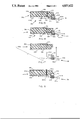
- One prior concept is to form an epoxy ring printed circuit probe card 30 with a set 32 of probes which are connected e.g. by solder 34 to conductive traces 36 formed on the bottom 38 of the card 30, as shown in FIGS. 1 and 2.
- An annular anodized aluminum ring 40 carries a cured shoulder formation 42 of epoxy resin which embeds and thereby aligns and secures the probes 32 in proper orientation and position.
- the probes 32 have a beam region or length 32a as measured from the inner wall 45 of the epoxy formation 42 to the probe taper or point 32b which is disposed at a predetermined angle relative to the horizontal, typically about seven degrees (7°).
- probe array comprising the aluminum ring 40, shoulder 42 and probe set 32 is preformed on a precise alignment fixture it is installed in an annular central opening 44 of the printed circuit card 30 and secured in place by a suitably curable epoxy resin 46.
- the prior art probe card 30 is generally in accordance with the disclosure of U.S. Pat. No. 3,905,098, for example.
- FIG. 3 A second prior concept, illustrated in FIG. 3, attempted to achieve higher density by combining the FIG. 1-2 approach with a second set 48 of probes connected to traces 50 formed on the top 52 of the card 30a by solder connections 54. After the first set 32 of probes is installed on the card 30, the second set 48 of probes is then installed by a second epoxy region 56 to the card 30a above the conventional probe ring 40.
- the second approach as illustrated in FIG. 3 has a number of drawbacks: it is difficult to construct. It will not easily meet the criteria for acceptable probe cards discussed above. For example, the probe tips 48b of the second set 48 attack the pads of the VLSI circuit at a much sharper angle than do the probes of the first set 32. The sharper angle of the beam region 48a of the second set 48 greatly increases the contact force applied to the pad, and reduces the amount of scrub.
- the contact force of the probes 48a will be different than the contact force of the probes 32a; hence, balanced contact force throughout the entire probe array is difficult to achieve. Planarization and alignment are also very difficult to achieve with the FIG. 3 approach, absent a highly complex fabrication fixture.
- FIG. 4 Another prior concept, illustrated by FIG. 4, calls for two sets of probes on the card, with a conventional probe array set 32 on the bottom 38 and with an array of probe-holding blades 58 connecting from printed circuit traces 50a on the upper surfaces to probes 60 held by the blades 58 near the VLSI chip, as diagrammed in the FIG. 4 sectional view.
- the probe needle holding blades 58 may be of the type described in U.S. Pat. No. 3,849,728, and may be soldered to the traces 50a along metalized lower edges as shown in FIG. 4.
- the blades 58 are made of metal, significant problems arise with the increase in capacitive coupling between probes such blade structures present. If the blades 58 are made of ceramic, they are very brittle and difficult to handle. Moreover, ceramic has proven unreliable because of the alignment and planarization problems introduced by the differences in coefficients of expansion between the ceramic or metal blade 58 and the tungsten probe wire 60, solder 62 and printed circuit trace materials 50a. It will be appreciated that the solder bead 62 required to secure the blade 58 to its corresponding trace 50a is vastly more elongated and extensive than the solder beads 36 used to connect each lower probe wire 32 to its corresponding lower trace 34.
- FIG. 5 Yet another prior concept, illustrated diagrammatically in FIG. 5, requires the use of two printed circuit boards, a so-called mother board 30c, and a so-called daughter board 30d.
- the mother board 30c carries the outer set of probes 63 in conventional fashion, and the daughter board 30d carries the inner set of probes 64.
- the daughter board 30d fits into an annular recess 68 formed in the mother board 30c, and a series of flexible conductive traces, held in place by a foam compression gasket 70 (metal on erastma) interconnect traces 72 on the top of the daughter board 30d to corresponding conductive traces 74 on the top of the mother board 30c.
- a foam compression gasket 70 metal on erastma
- An annular frog ring 73 supports the mother board 30c and is itself connected mechanically to an upper test card 30e.
- Pogo pins 76 provide electrical connections between traces on the lower surface of the test card 30e and the traces 74 of the mother board 30c.
- An inner annular housing 78 holds the daughter board 30d and the foamed connector 70 in place against the mother board 30c.
- An inner flange 80 of the frog ring 73 retains the inner housing 78 in place.
- One drawback of the multiple printed circuit board solution is its complexity. Another drawback is that the compression connection 70 may not prove to be reliable. A further drawback is that of impedance matching both sets of probes to a nominal impedance, such as 50 ohms or 93 ohms, the two standard impedances followed in the probe card industry.
- One other significant drawback is that the inner housing 78 makes it impossible to add certain needed circuit elements, preferably to the top of the daughter board 30d. These elements are typically small bypass capacitors, which are added to the probe arrays in the vicinity of the inner annular opening 44.
- the FIG. 5 arrangement additionally suffers from the significant drawback that the probe force applied by each of the probes 64 of the inner set is difficult to balance with the force applied by each of the probes 63 of the outer set.
- probe card 30f is illustrated in the FIG. 6A-6B drawing pair.
- This prior concept follows the concept outlined in connection with FIGS. 1 and 2, except that a higher density is achieved by staggering the probes of the probe array.
- the probes 32 are arranged into a lower row 32c and an upper row 32d which is offset radially and interleaved with the lower row 32c.
- the probe wires 32e extend radially outwardly to traces 34a on the lower surface 38 of the probe card 30f.
- the drawback and ultimate density limitation for the probe card 30f is that the traces 34a are formed on the same lower surface 38 and must be located at the same radial distance.
- the single set of traces carry all of the connections for all of the probes 32.
- they In order for there to be sufficient spacing for 256 to 320 radial traces 34a, they must be radially spaced from the central opening a sufficient distance to allow for minimum trace width and for insulative spacing between the traces.
- This means that the traces 34a are set back so far that the probe wires 32e extend a considreable distance in very close proximity. This close proximity leads directly to shorts and to undesirable coupling and electrical cross-talk between the probes.
- the probing equipment, the test head and its interface hardware dictate the size of the probe card to be used for testing the integrated circuit. More specifically, the test head and the test head interface hardware dictate the outer radial distances to which the probe traces can extend. These outer radial distances in turn limit the number of probes traces and the amount of space between those traces on a give circumference. With the limited size of the probe card and the limited radial distances of the probe traces from center, and with the resultant closeness of adjacent traces, it is extremely difficult to construct a high density probe card of the type illustrated in FIGS. 6A and 6B, due to the liklihood that adjacent probe wires, especially those at the corners of the integrated circuit, will contact one another and become shorted. This is especially true with a rectangular integrated circuit layout, or a square layout for an integrated circuit whose connection pads are not necessarily uniformly distributed along the sides.
- a general object of the present invention is to provide a probe card which overcomes the limitations and drawbacks of the prior art.
- One specific object of the present invention is to provide an improved epoxy ring probe card which effectively provides a higher number and density of individual test probes than heretofore achieved.
- a further object of the present invention is to provide an improved probe card assembly which provides radial circuit traces on two surfaces of the card in an interstitial spacing arrangement in order to facilitate fabrication and achieve higher numbers and densities of probes than heretofore.
- Another object of the present invention is to provide a high density probe card of two sets of probes, wherein each probe is matched in performance characteristics to the other probes, irrespective of which set the probe may be within.
- One more object of the present invention is to provide a high density probe card of two sets of probes wherein conductive traces on both surfaces of the card connect to both sets of probes in an arrangement providing matched impedances of e.g. 50 ohms, and low capacitive coupling, thereby enabling clocking speeds to reach 100 MHz and higher.
- a further object of the present invention is to provide a high density probe card of two sets of probes wherein the contact force of one set is balanced with the contact force of the other set, and the scrub of both sets is essentially the same distance.
- Yet another object of the present invention is to provide a high density probe card construction which facilitates access to all probe connections thereby enabling connection of additional electrical components, such as capacitors, resistors, and the like.
- One further object of the present invention is to provide an optimized high density probe card having more precisely controllable electrical impedance characteristics by virtue of the latitude provided by greater trace width for each trace, while at the same time providing sufficient working room for mechanical/electrical attachment of all of the probe wires to their respective traces.
- One more object of the present invention is to provide a high density probe card which is vastly simplified, less expensive, more reliable, more readily manufacturable and more readily reparable than prior high density probe cards.
- the probe card includes a unitary printed circuit board having a central opening adapted to receive a preformed array of probes.
- the board has a multiplicity of conductive traces, there being a first set of traces formed on a lower major surface thereof and a second set of traces formed on an upper major surface thereof, there being in total number at least as many traces as there are probes of said probe card.
- Feed through connectors are provided for feeding a connection for each upper trace through the printed circuit board to an inner annular region on the lower major surface of the printed circuit board adjacent said opening.
- the preformed probe array includes an annular frame, and two sets of spaced apart probes bonded to the annular frame e.g. by curable resin material.
- the probes are bonded in alignment position relative to respective connection pads formed on each of the identical dies of the wafer.
- the adjacent probes of both sets are substantially parallel with each other, one set of probes being adjacently spaced apart from the other set thereof.
- One set of probes is adapted for electrical connection to the first set of traces on the lower surface, and the other set of probes is adapted for electrical connection to the second set of traces on the upper surface of the printed circuit probe card, in all cases via the lower surface thereof.
- the second set of traces on the upper surface are interstitially arranged relative to the first set of traces on the lower surface
- the probe array includes a third set of conductive traces formed on the lower surface of the printed circuit board in the inner annular region.
- the feed through connectors include conductive bridges passing through the printed circuit board whereby each of the third set of traces becomes electrically connected to a corresponding trace of the second set of traces. Each of the other set of probes is then bonded to a corresponding one of the third set of traces.
- each of the first set of printed circuit traces includes a raised bonding region extending away from the lower major surface of the printed circuit probe card in order to facilitate spacing of the one set of probes away from the other set of probes in the region adjacently outside of the annular probe frame.
- the printed circuit probe card is formed with three layers of conductive traces: a first layer on the lower major surface on which the first set of traces is formed, a second layer on the upper surface on which the second set of traces is formed, and an intermediate third layer interconnected with the second layer via conductive bridges passing through the printed circuit board in the inner annular region.
- a third set of traces is formed in this intermediate third layer, and the inner annular region is removed in order to expose the third set of traces to which the other set of probes is connected.
- an array of openings is provided through the printed circuit probe card to provide for the feed through connectors extending from the lower inner annular region to the upper surface and for connecting with the second set of traces formed thereon.
- the feed through connectors comprise a series of pins secured to the other set of probes in alignment with openings formed through the printed circuit probe card, wherein the pins are adapted to be bonded to the second set of traces to establish electrical connection therewith.
- the feed through connectors comprise a vertically bent portion of each of the other set of probes.
- Each bent portion is prealigned with an opening formed through the printed circuit probe card.
- An upper terminous of each bent portion may then be bonded to the second set of traces in order to establish and maintain electrical connection therewith.
- FIG. 1 is a diagrammatic view in side elevation and section of a conventional low to medium density epoxy ring probe card as taught by the prior art, for example, U.S. Pat. No. 3,905,098, and as already discussed above.
- FIG. 2 is an enlarged diagrammatic view in side elevation and section of the prior art probe card shown in FIG. 1, along line 2--2.
- FIG. 3 is an enlarged diagrammatic view in side elevation and section of a portion of a second prior art high density probe card concept, already discussed above.
- FIG. 4 is an enlarged diagrammatic view in side elevation and section of a portion of a third prior art high density probe card concept, already discussed above.
- FIG. 5 is an enlarged diagrammatic view in side elevation and section of a portion of a fourth prior art high density probe card concept employing a mother board carrying a first set of probes and an inner annular daughter board carrying a second set of probes and which is nested with and retained by the mother board and other related support structure, as discussed above in greater detail.
- FIGS. 6A and 6B provide side section and bottom plan views of a fifth prior art higher density probe card in which all of the connection traces are formed on the lower surface of the probe card at the same radial length which is a substantial distance away from the probe array itself, as discussed above in greater detail.
- FIG. 7 is an enlarged bottom plan view of a relevant representative portion of a high density probe card incorporating the principles of the present invention, with some of the probes and traces not shown completely (the e.g. square locos of probe tip is shown) in order to save drawing room and thereby promote understanding of the present invention.
- FIG. 8 is a view in section and elevation of a portion of the probe card set forth in FIG. 7 taken along the line 8--8 in FIG. 7 and showing the interstitial relation between the first set of traces on the bottom side and the second set of traces on the top side of the probe printed circuit card.
- FIG. 9 is a diagrammatic view in side elevation and section of the high density probe card depicted in FIG. 7, with an integrated circuit wafer shown mounted on a wafer chuck, and with electrical connections to the probe card being made by pogo pin connectors, also shown diagramatically for illustration.
- FIG. 10 is a sectional view in side elevation of the high density probe card taken along the line 10--10 in FIG. 9.
- FIG. 11 is an enlarged bottom plan view of a rectangular probe array variant for inclusion in a high density probe card similar to the one depicted in FIGS. 7-10 in which the inner plan configuration of the annodized ring and epoxy is square rather than circular.
- FIG. 12 is a greatly enlarged view in perspective of the probe array depicted in FIG. 11 showing the alignment of two sets of staggered probes with corresponding staggered pads of an unsevered VLSI circuit formed on a wafer undergoing electrical testing via probe card contact.
- FIG. 13 is an enlarged diagrammatic view in side elevation and section of a portion of the probe array depicted in FIG. 12, taken along the line 13--13 in FIG. 12.
- FIG. 14 is an enlarged somewhat more diagramatic view in side elevation of a variant of the probe array depicted in FIGS. 11-13, wherein the contact pads of the unsevered VLSI circuit are in-line and wherein the two sets of probes are also in-line to match the pads.
- FIG. 15 is an enlarged diagrammatic view in side elevation and section of a portion of a variant of the the probe card depicted in FIGS. 7 through 10.
- FIG. 16 is an enlarged diagrammatic view in side elevation and section of a portion of another embodiment of a high density probe card incorporating the principles of the present invention.
- FIG. 17 is an enlarged and exploded diagrammatic view in side elevation and section of a portion of a further embodiment of a high density probe card incorporating the principles of the present invention.
- FIG. 18 is an enlarged diagrammatic view in side elevation and section of one more embodiment of a high density probe card incorporating the principles of the present invention.
- a high density epoxy ring probe card 130 is formed of a planar printed circuit board 131 and includes an array of a multiplicity of electrical contact providing probes 132 for engaging connection pads 133 of a very large scale integrated circuit 134 (shown by broken lines in FIG. 12) formed as one of many such circuits upon a major surface of a semiconductor wafer 136.
- the wafer 136 is supported upon a precision X-Y support stage 137.
- the wafer 136 is held to the stage 137 by the application of a vacuum through orifices formed through the stage 137 (not shown).
- the wafer 136 By conforming to the highly planarized support surface of the stage 137, the wafer 136 itself becomes highly planar and suitable for being contacted by the probes 132 of the card 130.
- the stage 137 is moved in the X and Y directions so that each VLSI circuit 134 may be properly registered in test position directly under the probes 132. After each circuit 134 is tested, it is passed or rejected, depending upon whether it meets the predetermined electrical performance specifications for the particular circuit being manufactured.
- the probe card 130 includes a preformed probe array 138 including an anodized aluminum ring 140, and an epoxy shoulder 142 in which the probes 132 are embedded and secured in predetermined proper alignment with the pads 133.
- the array ring 140 and the epoxy shoulder 142 carrying the probes 132 are secured in a grooved central annular opening 144 formed for the purpose of holding the array 138 by cured epoxy resin 146.
- the probe array 138 is of a high probe density, meaning that with the present invention, as many as 264 to 320 probes may be provided within the array 138.
- This high density means that there are at least 0.7 probes per degree of rotation about an imaginary axis extending through the center of the circuit 134 and normal to the surface thereof being probed by the probe card 130.
- the probe card 130 includes a bottom major surface 150 and a top major surface 152.
- the bottom major surface 150 is divided into three generally annular regions: an inner region 154 adjacent the probes 132 and central opening 144, a middle separation region 156 and an outer region 158.
- a series of radial connection pads or traces 160 is formed in the inner annular region 154.
- An annular ground shield 162 is disposed in the middle separation region 156, and a series of radial connection traces 164 is formed in the outer annular region 158.
- the separation region 156 physically separates the connection traces 160 of the inner annular region or zone 154 from the connection traces 164 of the outer annular region or zone 158, in addition to providing room for the ground shield trace 162.
- the probe array 138 or probes 132 is formed so that there are two rows of probes, a lower row 132a and an upper row 132b.
- the upper row 132b is horizontally offset relative to the lower row 132a so that each probe wire 132b of the upper row is spaced equally between the probe wires 132a of the lower row, and vice versa, as shown in FIG. 10.
- the radial connection traces 160 of the inner region 154 are equally spaced between the radial centers of the radial connection paths or traces 164 of the outer annular region 158.
- the probe wires of the upper row 132b are first attached to respective ones of the traces 160 of the inner annular region by solder connections 161, and the probe wires of the lower row 132a are subsequently attached to respective ones of the traces 164 of the outer annular region 158, also by solder connections 165.
- a series of radial connection paths or traces 166 is formed on the top major surface 152 of the probe card 130. Each of these traces is electrically connected to a radially aligned, corresponding pads or trace 160 of the inner annular region 154 of the lower surface by plated-through areas 168 bridging both surfaces 150 and 152 of the card 130.
- the traces 166 of the top surace 152 are spatially equally offset from the traces 164 of the bottom surface 150, as shown in FIG. 8. In this manner, the traces on both surfaces are provided with maximum isolation from each other and are subject to minimum inductive and/or capacitive cross-coupling and resultant cross-talk.
- the printed circuit board 131 forming the probe card 130 may be formed with an internal planar layer of metal such as copper for providing a continuous shield and ground plane 170.
- the ground plane 170 further isolates and shields the traces 166 of the top surface 152 from the traces 164 of the bottom surface.
- the annular shield 162 in the middle region 156 of the lower surface is electrically connected to the ground plane 170 by bridging regions 172 periodically spaced about the shield 162.
- the annular probe card 130 includes an array of connection locations 174 disposed in symmetrically aligned and spaced apart radial rows along the outer periphery of the upper surface 152. These connection locations enable the probe card 130 to be connected electrically with host equipment, preferably by "pogo pins" 176 as shown in FIG. 9. Some of the connection locations 174a are integral end portions of the connection traces 166 of the top surface 152. Others 174b of the connection locations are island regions which are connected to the connection traces 164 of the bottom surface 150 by plated through bridging areas 178. Still other locations 174c make direct electrical connection with the ground plane 170 and enable ground contacts to be interspersed with signal contacts at the other locations 174a and 174b.
- connection length for the probes 132b of the upper row of the array 138 to respective connection locations 174a is the same overall length as for the probes 132a of the lower row of the array to respective connection locations 174b. This result is perhaps best illustrated by the diagrammatic sectional view of FIG. 9. Equal length connections tend to equalize electrical characteristics, particularly transit times, which are so important for proper testing of very high speed VLSI circuitry with clocking cycles as high as 40 MHz to 100 MHz.
- a mylar mask is constructed which precisely follows the layout of the pads of the VLSI circuit 134 to be tested.
- a minute hole is formed in the mylar mask at the location of the center of each VLSI circuit connection pad 133.
- the mask is supported by an assembly drum which orients the probe wires and preliminarily holds them in place.
- a probe wire 132 typically of tungsten is formed with a tapered needle end depending downwardly to a contact point. The needle ends of the lower row 132a of probes are then placed through the outer holes of the mylar mask until all of the lower row 132a are in place and in proper alignment.
- an annulus of thin spacing material such as card stock, may be placed over the lower row 132a radially just beyond the vicinity of the supporting member.
- the upper row 132b of probes is installed with the needle ends thereof being precisely aligned by the mylar mask.
- curable epoxy resin of the same type is placed on the lower annular surface of the ring 140, and the epoxy coated supporting ring 140 is brought into contact to support the assembled probe array.
- the epoxy coating on the ring 140 flows into and unifies with the epoxy already emplaced in the array itself.
- the drum holding the assembled array is placed in an oven and cured at a curing temperature for an appropriate time period. Any excess epoxy is removed from the inner and outer annular surfaces, and assembly is then removed from the jig. The assembly is now ready to be connected to the probe card 130.
- the ring 140 is precisely oriented in the three relevant dimensions relative to the probe card 130 and is then glued to the probe card 130 in the central annular region 144, also preferably with a suitable thermosetting epoxy resin 146, as previously mentioned. After the resin 142 is cured, the individual probe wires 132 may then be soldered to their respective connection traces on the lower surface 150 of the probe card 130. In the embodiment of FIGS. 7-10 the upper row 132b of probes are soldered to their respective conductive traces 160 in the inner annular region 154 first, (with the lower row 132a probe wires bent slightly away from the bottom surface 150 to provide access to the wires of the upper row 132b).
- probe card 130 is then tested to check for alignment and planarity of the probes 132 and to be sure that there are no shorted probes or open or shorted circuits on the probe card itself. At this point construction of the probe card 130 is complete.
- the probes 132 vary somewhat in length, the shortest being those lying along a path which is the shortest distance from the edge of the VLSI circuit 134 being tested to the edge of the epoxy shoulder 142.
- a rectangular shoulder may prove to be advantageous, and such a shoulder 142a, supported by a modified ring 140a, is illustrated in FIGS. 11 and 12.
- the probe tip arrangement 138b is rectangular and the distances between the ring and shoulder and the probe tips are made to be virtually the same length for all probes of the array 138a.
- a cross section of this arrangement 138a, FIG. 13, shows that the probes 132b of the upper row extend beyond the probes 132a of the lower row.
- the length of the lower probes 132a from ring to probe tip is approximately 7 mils, while the length of the upper probes 132b from the ring to each tip is approxiamtely 17 mils.
- Both rows are disposed at a preferred angle of declination, e.g. seven degrees (7°). This arrangement accomodates the "checkerboard" pattern of connection pads 133 as seen in FIG. 12.
- connection pads of the VLSI circuit 134a are not staggered as in FIG. 12, but are in line.
- This arrangement 138b is illustrated in FIGS. 11 and 14.
- FIG. 15 provides a probe card 130a in which the traces 164a in the outer annular region 158 of the bottom surface 150 are formed to be thicker than the annular ground shield 162 and inner region traces 160. This height separation of the rearmost traces facilitates connection of the two rows 132a and 132b of the array 138, at some increased expense in the fabrication of the printed circuit 131a.
- the inner annular region 154a is countersunk, so that the inner traces 160a are separated in elevation from the outer traces 164.
- the inner trace 160 and fixed connection bridge 168 (as present in the FIG. 15 embodiment) has been replaced by a pin 200 which passes through a suitable opening through the printed circuit board 131c so that it may be soldered directly to the corresponding upper trace 166.
- the advantage of the pin arrangement is that the pins may be soldered to the upper row 132b of probe wires before the array 138 is glued to the probe card 130c with the use of a suitable jig enabling precise positioning of the pins 200.
- a probe 132b has to be replaced, it may be unsoldered from its pin, and removed from the epoxy shoulder 142. A replacement probe may then be inserted through the shoulder 142 and soldered to the radially elongated head 202 of the pin 200.
- the alternative probe card 130d illustrated in FIG. 18, is quite similar to the card 130c shown in FIG. 17, except that instead of the pin 200, the upper probe wires 132b are bent at precisely the correct distance away from the ring 140, and the bent portions 132c are then passed through suitable openings through the printed circuit board 131d and soldered directly to the upper traces 166.
Abstract
Description
Claims (2)
Priority Applications (1)
| Application Number | Priority Date | Filing Date | Title |
|---|---|---|---|
| US07/209,915 US4837622A (en) | 1985-05-10 | 1988-06-22 | High density probe card |
Applications Claiming Priority (2)
| Application Number | Priority Date | Filing Date | Title |
|---|---|---|---|
| US73350185A | 1985-05-10 | 1985-05-10 | |
| US07/209,915 US4837622A (en) | 1985-05-10 | 1988-06-22 | High density probe card |
Related Parent Applications (1)
| Application Number | Title | Priority Date | Filing Date |
|---|---|---|---|
| US07/045,605 Continuation US4757256A (en) | 1985-05-10 | 1987-05-01 | High density probe card |
Publications (1)
| Publication Number | Publication Date |
|---|---|
| US4837622A true US4837622A (en) | 1989-06-06 |
Family
ID=26904638
Family Applications (1)
| Application Number | Title | Priority Date | Filing Date |
|---|---|---|---|
| US07/209,915 Expired - Lifetime US4837622A (en) | 1985-05-10 | 1988-06-22 | High density probe card |
Country Status (1)
| Country | Link |
|---|---|
| US (1) | US4837622A (en) |
Cited By (70)
| Publication number | Priority date | Publication date | Assignee | Title |
|---|---|---|---|---|
| US5266059A (en) * | 1992-09-08 | 1993-11-30 | Hewlett-Packard Company | Generic rotatable connector assembly for testing integrated circuit packages |
| US5338223A (en) * | 1991-09-03 | 1994-08-16 | At&T Bell Laboratories | Hybrid wafer probe |
| US5382898A (en) * | 1992-09-21 | 1995-01-17 | Cerprobe Corporation | High density probe card for testing electrical circuits |
| US5444386A (en) * | 1992-01-17 | 1995-08-22 | Tokyo Seimitsu Co., Ltd. | Probing apparatus having an automatic probe card install mechanism and a semiconductor wafer testing system including the same |
| US5764072A (en) * | 1996-12-20 | 1998-06-09 | Probe Technology | Dual contact probe assembly for testing integrated circuits |
| US5820014A (en) | 1993-11-16 | 1998-10-13 | Form Factor, Inc. | Solder preforms |
| WO1998047010A1 (en) * | 1997-04-17 | 1998-10-22 | Cerprobe Corporation | Probe assembly and method for switchable multi-dut testing of integrated circuit wafers |
| US5917330A (en) * | 1996-01-17 | 1999-06-29 | Miley; David M. | Probe ring having electrical components affixed thereto and related apparatus and processes |
| US5949244A (en) * | 1996-01-03 | 1999-09-07 | Miley; David M. | Low tolerance probe card and probe ring systems |
| US5982187A (en) * | 1993-07-01 | 1999-11-09 | Alphatest Corporation | Resilient connector having a tubular spring |
| US5994152A (en) | 1996-02-21 | 1999-11-30 | Formfactor, Inc. | Fabricating interconnects and tips using sacrificial substrates |
| WO2000050905A1 (en) * | 1999-02-25 | 2000-08-31 | Formfactor, Inc. | High bandwidth passive integrated circuit tester probe card assembly |
| US6274823B1 (en) | 1993-11-16 | 2001-08-14 | Formfactor, Inc. | Interconnection substrates with resilient contact structures on both sides |
| US20010015652A1 (en) * | 1993-11-16 | 2001-08-23 | Formfactor, Inc. | Probe card assembly and kit, and methods of making same |
| US20010020747A1 (en) * | 1998-12-31 | 2001-09-13 | Formfactor, Inc. | Special contact points for accessing internal circuitry of an integrated circuit |
| US20010054905A1 (en) * | 1993-11-16 | 2001-12-27 | Igor Y. Khandros | Probe card assembly and kit |
| US6362642B1 (en) * | 1997-10-09 | 2002-03-26 | Micron Technology, Inc. | Method of chip testing of chip leads constrained in dielectric media |
| EP1202337A2 (en) * | 2000-10-24 | 2002-05-02 | Nec Corporation | Probe pin for a probe card |
| US6448865B1 (en) | 1999-02-25 | 2002-09-10 | Formfactor, Inc. | Integrated circuit interconnect system |
| US20020132501A1 (en) * | 2001-03-16 | 2002-09-19 | Eldridge Benjamin N. | Wafer level interposer |
| US6459343B1 (en) | 1999-02-25 | 2002-10-01 | Formfactor, Inc. | Integrated circuit interconnect system forming a multi-pole filter |
| US20020197895A1 (en) * | 1999-08-17 | 2002-12-26 | Formfactor, Inc. | Electrical contractor, especially wafer level contactor, using fluid pressure |
| US6499216B1 (en) | 1994-07-07 | 2002-12-31 | Tessera, Inc. | Methods and structures for electronic probing arrays |
| US20030010976A1 (en) * | 2001-07-11 | 2003-01-16 | Formfactor, Inc. | Method of manufacturing a probe card |
| US6515358B1 (en) * | 1997-09-30 | 2003-02-04 | Intel Corporation | Integrated passivation process, probe geometry and probing process |
| US6525555B1 (en) | 1993-11-16 | 2003-02-25 | Formfactor, Inc. | Wafer-level burn-in and test |
| US6586955B2 (en) | 2000-03-13 | 2003-07-01 | Tessera, Inc. | Methods and structures for electronic probing arrays |
| US6606014B2 (en) | 1999-02-25 | 2003-08-12 | Formfactor, Inc. | Filter structures for integrated circuit interfaces |
| US6618787B2 (en) * | 2000-12-14 | 2003-09-09 | Hewlett-Packard Development Company, L.P. | Computer printed circuit system board with LVD SCSI device direct connector |
| US6640415B2 (en) | 1999-06-07 | 2003-11-04 | Formfactor, Inc. | Segmented contactor |
| US20040022042A1 (en) * | 1999-07-28 | 2004-02-05 | Sammy Mok | Construction structures and manufacturing processes for integrated circuit wafer probe card assemblies |
| US6690185B1 (en) | 1997-01-15 | 2004-02-10 | Formfactor, Inc. | Large contactor with multiple, aligned contactor units |
| US6690186B2 (en) | 1994-07-07 | 2004-02-10 | Tessera, Inc. | Methods and structures for electronic probing arrays |
| US6720501B1 (en) | 1998-04-14 | 2004-04-13 | Formfactor, Inc. | PC board having clustered blind vias |
| US20040075455A1 (en) * | 2002-07-15 | 2004-04-22 | Sammy Mok | Mosaic decal probe |
| US6741085B1 (en) | 1993-11-16 | 2004-05-25 | Formfactor, Inc. | Contact carriers (tiles) for populating larger substrates with spring contacts |
| US6856150B2 (en) | 2001-04-10 | 2005-02-15 | Formfactor, Inc. | Probe card with coplanar daughter card |
| US20050051353A1 (en) * | 1999-05-27 | 2005-03-10 | Chong Fu Chiung | Massively parallel interface for electronic circuit |
| US20050068054A1 (en) * | 2000-05-23 | 2005-03-31 | Sammy Mok | Standardized layout patterns and routing structures for integrated circuit wafer probe card assemblies |
| US20050146339A1 (en) * | 2001-07-11 | 2005-07-07 | Formfactor, Inc. | Method of manufacturing a probe card |
| WO2006014635A1 (en) * | 2004-07-21 | 2006-02-09 | K & S Interconnect, Inc. | Reinforced probes for testing semiconductor devices |
| US20060033516A1 (en) * | 2000-08-24 | 2006-02-16 | Rincon Reynaldo M | Multiple-chip probe and universal tester contact assemblage |
| US20060043984A1 (en) * | 2004-08-25 | 2006-03-02 | Deborah Miller | Bottom side stiffener probe card |
| US20060145713A1 (en) * | 2005-01-03 | 2006-07-06 | Henson Roy J | Probe head arrays |
| US20080048688A1 (en) * | 2000-03-17 | 2008-02-28 | Formfactor, Inc. | Methods for planarizing a semiconductor contactor |
| US7349223B2 (en) | 2000-05-23 | 2008-03-25 | Nanonexus, Inc. | Enhanced compliant probe card systems having improved planarity |
| US20080122469A1 (en) * | 2006-11-28 | 2008-05-29 | Visera Technologies, Company Ltd. | Probe card for testing image-sensing chips |
| US7382142B2 (en) | 2000-05-23 | 2008-06-03 | Nanonexus, Inc. | High density interconnect system having rapid fabrication cycle |
| US20080136429A1 (en) * | 2006-12-12 | 2008-06-12 | Samsung Electronics Co., Ltd. | Probe card of semiconductor test apparatus and method of fabricating the same |
| US20080136432A1 (en) * | 2006-12-06 | 2008-06-12 | Formfactor, Inc. | Sharing resources in a system for testing semiconductor devices |
| US20090079448A1 (en) * | 2007-09-25 | 2009-03-26 | Formfactor, Inc. | Method And Apparatus For Testing Devices Using Serially Controlled Resources |
| US20090085590A1 (en) * | 2007-09-27 | 2009-04-02 | Formfactor, Inc. | Method And Apparatus For Testing Devices Using Serially Controlled Intelligent Switches |
| US20090146675A1 (en) * | 2007-12-10 | 2009-06-11 | Touchdown Technologies, Inc. | Planarizing probe card |
| US20090164931A1 (en) * | 2007-12-19 | 2009-06-25 | Formfactor, Inc. | Method and Apparatus for Managing Test Result Data Generated by a Semiconductor Test System |
| US20090174423A1 (en) * | 2004-07-21 | 2009-07-09 | Klaerner Peter J | Bond Reinforcement Layer for Probe Test Cards |
| US7579848B2 (en) | 2000-05-23 | 2009-08-25 | Nanonexus, Inc. | High density interconnect system for IC packages and interconnect assemblies |
| US20090224793A1 (en) * | 2008-03-07 | 2009-09-10 | Formfactor, Inc. | Method And Apparatus For Designing A Custom Test System |
| US20090235131A1 (en) * | 2008-03-11 | 2009-09-17 | Formfactor, Inc. | Method and apparatus for processing failures during semiconductor device testing |
| US7621761B2 (en) | 2000-06-20 | 2009-11-24 | Nanonexus, Inc. | Systems for testing and packaging integrated circuits |
| US7649366B2 (en) | 2006-09-01 | 2010-01-19 | Formfactor, Inc. | Method and apparatus for switching tester resources |
| US20100050029A1 (en) * | 2008-08-19 | 2010-02-25 | Formfactor, Inc. | Method And Apparatus For Testing Semiconductor Devices With Autonomous Expected Value Generation |
| US7786744B2 (en) | 2008-11-04 | 2010-08-31 | King Yuan Electronics Co., Ltd. | Probe card assembly and test probes therein |
| US20110057018A1 (en) * | 1995-05-26 | 2011-03-10 | Formfactor, Inc. | Method of wirebonding that utilizes a gas flow within a capillary from which a wire is played out |
| US7944225B2 (en) | 2008-09-26 | 2011-05-17 | Formfactor, Inc. | Method and apparatus for providing a tester integrated circuit for testing a semiconductor device under test |
| US7952373B2 (en) | 2000-05-23 | 2011-05-31 | Verigy (Singapore) Pte. Ltd. | Construction structures and manufacturing processes for integrated circuit wafer probe card assemblies |
| US8033838B2 (en) | 1996-02-21 | 2011-10-11 | Formfactor, Inc. | Microelectronic contact structure |
| US8373428B2 (en) | 1993-11-16 | 2013-02-12 | Formfactor, Inc. | Probe card assembly and kit, and methods of making same |
| ITMI20120453A1 (en) * | 2012-03-22 | 2013-09-23 | Technoprobe Spa | HYBRID TYPE CONNECTION STRUCTURE |
| US20140103948A1 (en) * | 2010-03-11 | 2014-04-17 | Mpi Corporation | Probe card having configurable structure for exchanging or swapping electronic components for impedance matching |
| US11379004B2 (en) * | 2018-08-08 | 2022-07-05 | Hewlett-Packard Development Company, L.P. | Adjustment control mechanisms of pogo pins |
Citations (5)
| Publication number | Priority date | Publication date | Assignee | Title |
|---|---|---|---|---|
| US3835387A (en) * | 1972-11-15 | 1974-09-10 | Columbia Pictures Ind Inc | Control circuitry for information transmission system |
| JPS5523437A (en) * | 1978-08-09 | 1980-02-19 | Nippon Denshi Zairyo Kk | Manufacture of prove unit for semiconductor wafer test |
| JPS5872060A (en) * | 1981-10-26 | 1983-04-28 | Nippon Denshi Zairyo Kk | Probe card |
| US4480223A (en) * | 1981-11-25 | 1984-10-30 | Seiichiro Aigo | Unitary probe assembly |
| US4523144A (en) * | 1980-05-27 | 1985-06-11 | Japan Electronic Materials Corp. | Complex probe card for testing a semiconductor wafer |
-
1988
- 1988-06-22 US US07/209,915 patent/US4837622A/en not_active Expired - Lifetime
Patent Citations (5)
| Publication number | Priority date | Publication date | Assignee | Title |
|---|---|---|---|---|
| US3835387A (en) * | 1972-11-15 | 1974-09-10 | Columbia Pictures Ind Inc | Control circuitry for information transmission system |
| JPS5523437A (en) * | 1978-08-09 | 1980-02-19 | Nippon Denshi Zairyo Kk | Manufacture of prove unit for semiconductor wafer test |
| US4523144A (en) * | 1980-05-27 | 1985-06-11 | Japan Electronic Materials Corp. | Complex probe card for testing a semiconductor wafer |
| JPS5872060A (en) * | 1981-10-26 | 1983-04-28 | Nippon Denshi Zairyo Kk | Probe card |
| US4480223A (en) * | 1981-11-25 | 1984-10-30 | Seiichiro Aigo | Unitary probe assembly |
Cited By (157)
| Publication number | Priority date | Publication date | Assignee | Title |
|---|---|---|---|---|
| US5338223A (en) * | 1991-09-03 | 1994-08-16 | At&T Bell Laboratories | Hybrid wafer probe |
| US5444386A (en) * | 1992-01-17 | 1995-08-22 | Tokyo Seimitsu Co., Ltd. | Probing apparatus having an automatic probe card install mechanism and a semiconductor wafer testing system including the same |
| DE4315082A1 (en) * | 1992-09-08 | 1994-03-10 | Hewlett Packard Co | Versatile rotatable connector assembly for testing integrated circuit components |
| US5266059A (en) * | 1992-09-08 | 1993-11-30 | Hewlett-Packard Company | Generic rotatable connector assembly for testing integrated circuit packages |
| US5382898A (en) * | 1992-09-21 | 1995-01-17 | Cerprobe Corporation | High density probe card for testing electrical circuits |
| US5982187A (en) * | 1993-07-01 | 1999-11-09 | Alphatest Corporation | Resilient connector having a tubular spring |
| US20070075715A1 (en) * | 1993-11-16 | 2007-04-05 | Formfactor, Inc. | Contact Carriers (Tiles) For Populating Larger Substrates With Spring Contacts |
| US6788094B2 (en) | 1993-11-16 | 2004-09-07 | Formfactor, Inc. | Wafer-level burn-in and test |
| US20080180121A1 (en) * | 1993-11-16 | 2008-07-31 | Formfactor, Inc. | Probe card assembly and kit |
| US20080231305A1 (en) * | 1993-11-16 | 2008-09-25 | Formfactor, Inc. | Contact carriers (tiles) for populating larger substrates with spring contacts |
| US5820014A (en) | 1993-11-16 | 1998-10-13 | Form Factor, Inc. | Solder preforms |
| US20040163252A1 (en) * | 1993-11-16 | 2004-08-26 | Formfactor, Inc. | Contact carriers (tiles) for populating larger substrates with spring contacts |
| US7064566B2 (en) | 1993-11-16 | 2006-06-20 | Formfactor, Inc. | Probe card assembly and kit |
| US7078926B2 (en) | 1993-11-16 | 2006-07-18 | Formfactor, Inc. | Wafer-level burn-in and test |
| US6274823B1 (en) | 1993-11-16 | 2001-08-14 | Formfactor, Inc. | Interconnection substrates with resilient contact structures on both sides |
| US20010015652A1 (en) * | 1993-11-16 | 2001-08-23 | Formfactor, Inc. | Probe card assembly and kit, and methods of making same |
| US7086149B2 (en) | 1993-11-16 | 2006-08-08 | Formfactor, Inc. | Method of making a contact structure with a distinctly formed tip structure |
| US20010054905A1 (en) * | 1993-11-16 | 2001-12-27 | Igor Y. Khandros | Probe card assembly and kit |
| US7061257B2 (en) | 1993-11-16 | 2006-06-13 | Formfactor, Inc. | Probe card assembly |
| US7616016B2 (en) | 1993-11-16 | 2009-11-10 | Formfactor, Inc. | Probe card assembly and kit |
| US7140883B2 (en) | 1993-11-16 | 2006-11-28 | Formfactor, Inc. | Contact carriers (tiles) for populating larger substrates with spring contacts |
| US20070013401A1 (en) * | 1993-11-16 | 2007-01-18 | Formfactor, Inc. | Wafer-level burn-in and test |
| US8373428B2 (en) | 1993-11-16 | 2013-02-12 | Formfactor, Inc. | Probe card assembly and kit, and methods of making same |
| US7688090B2 (en) | 1993-11-16 | 2010-03-30 | Formfactor, Inc. | Wafer-level burn-in and test |
| US6741085B1 (en) | 1993-11-16 | 2004-05-25 | Formfactor, Inc. | Contact carriers (tiles) for populating larger substrates with spring contacts |
| US7345493B2 (en) | 1993-11-16 | 2008-03-18 | Formfactor, Inc. | Wafer-level burn-in and test |
| US20050035347A1 (en) * | 1993-11-16 | 2005-02-17 | Khandros Igor Y. | Probe card assembly |
| US20030222667A1 (en) * | 1993-11-16 | 2003-12-04 | Formfactor, Inc. | Probe card assembly |
| US7347702B2 (en) | 1993-11-16 | 2008-03-25 | Formfactor, Inc. | Contact carriers (tiles) for populating larger substrates with spring contacts |
| US7714598B2 (en) | 1993-11-16 | 2010-05-11 | Formfactor, Inc. | Contact carriers (tiles) for populating larger substrates with spring contacts |
| US20080157808A1 (en) * | 1993-11-16 | 2008-07-03 | Formfactor, Inc. | Wafer-level burn-in and test |
| US20050017750A1 (en) * | 1993-11-16 | 2005-01-27 | Formfactor, Inc. | Wafer-level burn-in and test |
| US6525555B1 (en) | 1993-11-16 | 2003-02-25 | Formfactor, Inc. | Wafer-level burn-in and test |
| US20030107394A1 (en) * | 1993-11-16 | 2003-06-12 | Formfactor, Inc. | Wafer-level burn-in and test |
| US6838893B2 (en) | 1993-11-16 | 2005-01-04 | Formfactor, Inc. | Probe card assembly |
| US7352196B2 (en) | 1993-11-16 | 2008-04-01 | Formfactor, Inc. | Probe card assembly and kit |
| US6499216B1 (en) | 1994-07-07 | 2002-12-31 | Tessera, Inc. | Methods and structures for electronic probing arrays |
| US6690186B2 (en) | 1994-07-07 | 2004-02-10 | Tessera, Inc. | Methods and structures for electronic probing arrays |
| US20110057018A1 (en) * | 1995-05-26 | 2011-03-10 | Formfactor, Inc. | Method of wirebonding that utilizes a gas flow within a capillary from which a wire is played out |
| US8485418B2 (en) | 1995-05-26 | 2013-07-16 | Formfactor, Inc. | Method of wirebonding that utilizes a gas flow within a capillary from which a wire is played out |
| US5949244A (en) * | 1996-01-03 | 1999-09-07 | Miley; David M. | Low tolerance probe card and probe ring systems |
| US5917330A (en) * | 1996-01-17 | 1999-06-29 | Miley; David M. | Probe ring having electrical components affixed thereto and related apparatus and processes |
| US8033838B2 (en) | 1996-02-21 | 2011-10-11 | Formfactor, Inc. | Microelectronic contact structure |
| US5994152A (en) | 1996-02-21 | 1999-11-30 | Formfactor, Inc. | Fabricating interconnects and tips using sacrificial substrates |
| US5764072A (en) * | 1996-12-20 | 1998-06-09 | Probe Technology | Dual contact probe assembly for testing integrated circuits |
| US6690185B1 (en) | 1997-01-15 | 2004-02-10 | Formfactor, Inc. | Large contactor with multiple, aligned contactor units |
| WO1998047010A1 (en) * | 1997-04-17 | 1998-10-22 | Cerprobe Corporation | Probe assembly and method for switchable multi-dut testing of integrated circuit wafers |
| US6515358B1 (en) * | 1997-09-30 | 2003-02-04 | Intel Corporation | Integrated passivation process, probe geometry and probing process |
| US6362642B1 (en) * | 1997-10-09 | 2002-03-26 | Micron Technology, Inc. | Method of chip testing of chip leads constrained in dielectric media |
| US6384426B1 (en) | 1997-10-09 | 2002-05-07 | Micron Technology, Inc. | System for testing semiconductor chip leads constrained in dielectric media |
| US6720501B1 (en) | 1998-04-14 | 2004-04-13 | Formfactor, Inc. | PC board having clustered blind vias |
| US6839964B2 (en) | 1998-04-14 | 2005-01-11 | Formfactor, Inc. | Method for manufacturing a multi-layer printed circuit board |
| US20010020747A1 (en) * | 1998-12-31 | 2001-09-13 | Formfactor, Inc. | Special contact points for accessing internal circuitry of an integrated circuit |
| US6603324B2 (en) | 1998-12-31 | 2003-08-05 | Formfactor, Inc. | Special contact points for accessing internal circuitry of an integrated circuit |
| US6597187B2 (en) | 1998-12-31 | 2003-07-22 | Formfactor, Inc. | Special contact points for accessing internal circuitry of an integrated circuit |
| US6940093B2 (en) | 1998-12-31 | 2005-09-06 | Formfactor, Inc. | Special contact points for accessing internal circuitry of an integrated circuit |
| US6456099B1 (en) * | 1998-12-31 | 2002-09-24 | Formfactor, Inc. | Special contact points for accessing internal circuitry of an integrated circuit |
| US6459343B1 (en) | 1999-02-25 | 2002-10-01 | Formfactor, Inc. | Integrated circuit interconnect system forming a multi-pole filter |
| US20110115512A1 (en) * | 1999-02-25 | 2011-05-19 | Formfactor, Inc. | Integrated circuit tester with high bandwidth probe assembly |
| US6501343B2 (en) * | 1999-02-25 | 2002-12-31 | Formfactor, Inc. | Integrated circuit tester with high bandwidth probe assembly |
| KR100793501B1 (en) | 1999-02-25 | 2008-01-14 | 폼팩터, 인크. | High bandwidth passive integrated circuit tester probe card assembly |
| US6448865B1 (en) | 1999-02-25 | 2002-09-10 | Formfactor, Inc. | Integrated circuit interconnect system |
| US6606014B2 (en) | 1999-02-25 | 2003-08-12 | Formfactor, Inc. | Filter structures for integrated circuit interfaces |
| US6218910B1 (en) * | 1999-02-25 | 2001-04-17 | Formfactor, Inc. | High bandwidth passive integrated circuit tester probe card assembly |
| WO2000050905A1 (en) * | 1999-02-25 | 2000-08-31 | Formfactor, Inc. | High bandwidth passive integrated circuit tester probe card assembly |
| US20050051353A1 (en) * | 1999-05-27 | 2005-03-10 | Chong Fu Chiung | Massively parallel interface for electronic circuit |
| US7884634B2 (en) | 1999-05-27 | 2011-02-08 | Verigy (Singapore) Pte, Ltd | High density interconnect system having rapid fabrication cycle |
| US7772860B2 (en) | 1999-05-27 | 2010-08-10 | Nanonexus, Inc. | Massively parallel interface for electronic circuit |
| US7403029B2 (en) | 1999-05-27 | 2008-07-22 | Nanonexus Corporation | Massively parallel interface for electronic circuit |
| US7009412B2 (en) | 1999-05-27 | 2006-03-07 | Nanonexus, Inc. | Massively parallel interface for electronic circuit |
| US6640415B2 (en) | 1999-06-07 | 2003-11-04 | Formfactor, Inc. | Segmented contactor |
| US8011089B2 (en) | 1999-06-07 | 2011-09-06 | Formfactor, Inc. | Method of repairing segmented contactor |
| US20040058487A1 (en) * | 1999-06-07 | 2004-03-25 | Formfactor, Inc. | Segmented contactor |
| US7065870B2 (en) | 1999-06-07 | 2006-06-27 | Formfactor, Inc. | Segmented contactor |
| US7578057B2 (en) | 1999-06-07 | 2009-08-25 | Formfactor, Inc. | Method of fabricating segmented contactor |
| US7215131B1 (en) | 1999-06-07 | 2007-05-08 | Formfactor, Inc. | Segmented contactor |
| US20100043226A1 (en) * | 1999-06-07 | 2010-02-25 | Formfactor, Inc. | Segmented contactor |
| US6815961B2 (en) | 1999-07-28 | 2004-11-09 | Nanonexus, Inc. | Construction structures and manufacturing processes for integrated circuit wafer probe card assemblies |
| US20040022042A1 (en) * | 1999-07-28 | 2004-02-05 | Sammy Mok | Construction structures and manufacturing processes for integrated circuit wafer probe card assemblies |
| US7722371B2 (en) | 1999-08-17 | 2010-05-25 | Formfactor, Inc. | Electrical contactor, especially wafer level contactor, using fluid pressure |
| US7967621B2 (en) | 1999-08-17 | 2011-06-28 | Formfactor, Inc. | Electrical contactor, especially wafer level contactor, using fluid pressure |
| US7195503B2 (en) | 1999-08-17 | 2007-03-27 | Formfactor, Inc. | Electrical contactor, especially wafer level contactor, using fluid pressure |
| US20070287304A1 (en) * | 1999-08-17 | 2007-12-13 | Formfactor, Inc. | Electrical Contactor, Espcecially Wafer Level Contactor, Using Fluid Pressure |
| US7455540B2 (en) | 1999-08-17 | 2008-11-25 | Formfactor, Inc. | Electrical contactor, especially wafer level contactor, using fluid pressure |
| US20100297863A1 (en) * | 1999-08-17 | 2010-11-25 | Formfactor, Inc. | Electrical contactor, especially wafer level contactor, using fluid pressure |
| US20020197895A1 (en) * | 1999-08-17 | 2002-12-26 | Formfactor, Inc. | Electrical contractor, especially wafer level contactor, using fluid pressure |
| US20090072848A1 (en) * | 1999-08-17 | 2009-03-19 | Formfactor, Inc. | Electrical Contactor, Especially Wafer Level Contactor, Using Fluid Pressure |
| US6586955B2 (en) | 2000-03-13 | 2003-07-01 | Tessera, Inc. | Methods and structures for electronic probing arrays |
| US20080048688A1 (en) * | 2000-03-17 | 2008-02-28 | Formfactor, Inc. | Methods for planarizing a semiconductor contactor |
| US20100263432A1 (en) * | 2000-03-17 | 2010-10-21 | Formfactor, Inc. | Methods for planarizing a semiconductor contactor |
| US8427183B2 (en) | 2000-03-17 | 2013-04-23 | Formfactor, Inc. | Probe card assembly having an actuator for bending the probe substrate |
| US7737709B2 (en) | 2000-03-17 | 2010-06-15 | Formfactor, Inc. | Methods for planarizing a semiconductor contactor |
| US20110193583A1 (en) * | 2000-03-17 | 2011-08-11 | Formfactor, Inc. | Methods for planarizing a semiconductor contactor |
| US7349223B2 (en) | 2000-05-23 | 2008-03-25 | Nanonexus, Inc. | Enhanced compliant probe card systems having improved planarity |
| US7579848B2 (en) | 2000-05-23 | 2009-08-25 | Nanonexus, Inc. | High density interconnect system for IC packages and interconnect assemblies |
| US7382142B2 (en) | 2000-05-23 | 2008-06-03 | Nanonexus, Inc. | High density interconnect system having rapid fabrication cycle |
| US7952373B2 (en) | 2000-05-23 | 2011-05-31 | Verigy (Singapore) Pte. Ltd. | Construction structures and manufacturing processes for integrated circuit wafer probe card assemblies |
| US7872482B2 (en) | 2000-05-23 | 2011-01-18 | Verigy (Singapore) Pte. Ltd | High density interconnect system having rapid fabrication cycle |
| US20050068054A1 (en) * | 2000-05-23 | 2005-03-31 | Sammy Mok | Standardized layout patterns and routing structures for integrated circuit wafer probe card assemblies |
| US7621761B2 (en) | 2000-06-20 | 2009-11-24 | Nanonexus, Inc. | Systems for testing and packaging integrated circuits |
| US20060033516A1 (en) * | 2000-08-24 | 2006-02-16 | Rincon Reynaldo M | Multiple-chip probe and universal tester contact assemblage |
| US7026833B2 (en) * | 2000-08-24 | 2006-04-11 | Texas Instruments Incorporated | Multiple-chip probe and universal tester contact assemblage |
| EP1202337A2 (en) * | 2000-10-24 | 2002-05-02 | Nec Corporation | Probe pin for a probe card |
| US6812723B2 (en) | 2000-10-24 | 2004-11-02 | Nec Electronics Corporation | Probe pin for a probe card |
| EP1202337A3 (en) * | 2000-10-24 | 2002-09-18 | Nec Corporation | Probe pin for a probe card |
| US6618787B2 (en) * | 2000-12-14 | 2003-09-09 | Hewlett-Packard Development Company, L.P. | Computer printed circuit system board with LVD SCSI device direct connector |
| US20020132501A1 (en) * | 2001-03-16 | 2002-09-19 | Eldridge Benjamin N. | Wafer level interposer |
| US7649368B2 (en) | 2001-03-16 | 2010-01-19 | Formfactor, Inc. | Wafer level interposer |
| US7396236B2 (en) | 2001-03-16 | 2008-07-08 | Formfactor, Inc. | Wafer level interposer |
| US7116119B2 (en) | 2001-04-10 | 2006-10-03 | Formfactor, Inc. | Probe card with coplanar daughter card |
| US6856150B2 (en) | 2001-04-10 | 2005-02-15 | Formfactor, Inc. | Probe card with coplanar daughter card |
| US20050140381A1 (en) * | 2001-04-10 | 2005-06-30 | Formfactor, Inc. | Probe card with coplanar daughter card |
| US20030025172A1 (en) * | 2001-07-11 | 2003-02-06 | Formfactor, Inc. | Method of manufacturing a probe card |
| US20030010976A1 (en) * | 2001-07-11 | 2003-01-16 | Formfactor, Inc. | Method of manufacturing a probe card |
| US20050146339A1 (en) * | 2001-07-11 | 2005-07-07 | Formfactor, Inc. | Method of manufacturing a probe card |
| US7168162B2 (en) | 2001-07-11 | 2007-01-30 | Formfactor, Inc. | Method of manufacturing a probe card |
| US7196531B2 (en) * | 2001-07-11 | 2007-03-27 | Formfactor, Inc. | Method of manufacturing a probe card |
| US7948252B2 (en) | 2001-07-11 | 2011-05-24 | Formfactor, Inc. | Multilayered probe card |
| US20070126443A1 (en) * | 2001-07-11 | 2007-06-07 | Formfactor, Inc. | Method of Manufacturing A Probe Card |
| US7400157B2 (en) | 2001-07-11 | 2008-07-15 | Formfactor, Inc. | Composite wiring structure having a wiring block and an insulating layer with electrical connections to probes |
| US20070247176A1 (en) * | 2001-07-11 | 2007-10-25 | Formfactor, Inc. | Method of Manufacturing a Probe Card |
| US20080272794A1 (en) * | 2001-07-11 | 2008-11-06 | Formfactor, Inc.. | Method of manufacturing a probe card |
| US6864105B2 (en) | 2001-07-11 | 2005-03-08 | Formfactor, Inc. | Method of manufacturing a probe card |
| US20040194299A1 (en) * | 2001-07-11 | 2004-10-07 | Formfactor, Inc. | Method of manufacturing a probe card |
| US6729019B2 (en) | 2001-07-11 | 2004-05-04 | Formfactor, Inc. | Method of manufacturing a probe card |
| US20040075455A1 (en) * | 2002-07-15 | 2004-04-22 | Sammy Mok | Mosaic decal probe |
| WO2006014635A1 (en) * | 2004-07-21 | 2006-02-09 | K & S Interconnect, Inc. | Reinforced probes for testing semiconductor devices |
| US20060028220A1 (en) * | 2004-07-21 | 2006-02-09 | K&S Interconnect, Inc. | Reinforced probes for testing semiconductor devices |
| US20090174423A1 (en) * | 2004-07-21 | 2009-07-09 | Klaerner Peter J | Bond Reinforcement Layer for Probe Test Cards |
| US20060043984A1 (en) * | 2004-08-25 | 2006-03-02 | Deborah Miller | Bottom side stiffener probe card |
| US7218130B2 (en) * | 2004-08-25 | 2007-05-15 | Micron Technology, Inc. | Bottom side stiffener probe card |
| US7282933B2 (en) | 2005-01-03 | 2007-10-16 | Formfactor, Inc. | Probe head arrays |
| US20060145713A1 (en) * | 2005-01-03 | 2006-07-06 | Henson Roy J | Probe head arrays |
| US7649366B2 (en) | 2006-09-01 | 2010-01-19 | Formfactor, Inc. | Method and apparatus for switching tester resources |
| US20080122469A1 (en) * | 2006-11-28 | 2008-05-29 | Visera Technologies, Company Ltd. | Probe card for testing image-sensing chips |
| US7852094B2 (en) | 2006-12-06 | 2010-12-14 | Formfactor, Inc. | Sharing resources in a system for testing semiconductor devices |
| US20080136432A1 (en) * | 2006-12-06 | 2008-06-12 | Formfactor, Inc. | Sharing resources in a system for testing semiconductor devices |
| US20080136429A1 (en) * | 2006-12-12 | 2008-06-12 | Samsung Electronics Co., Ltd. | Probe card of semiconductor test apparatus and method of fabricating the same |
| US7888955B2 (en) | 2007-09-25 | 2011-02-15 | Formfactor, Inc. | Method and apparatus for testing devices using serially controlled resources |
| US20090079448A1 (en) * | 2007-09-25 | 2009-03-26 | Formfactor, Inc. | Method And Apparatus For Testing Devices Using Serially Controlled Resources |
| US7977959B2 (en) | 2007-09-27 | 2011-07-12 | Formfactor, Inc. | Method and apparatus for testing devices using serially controlled intelligent switches |
| US8872534B2 (en) | 2007-09-27 | 2014-10-28 | Formfactor, Inc. | Method and apparatus for testing devices using serially controlled intelligent switches |
| US20090085590A1 (en) * | 2007-09-27 | 2009-04-02 | Formfactor, Inc. | Method And Apparatus For Testing Devices Using Serially Controlled Intelligent Switches |
| US20090146675A1 (en) * | 2007-12-10 | 2009-06-11 | Touchdown Technologies, Inc. | Planarizing probe card |
| US7791361B2 (en) | 2007-12-10 | 2010-09-07 | Touchdown Technologies, Inc. | Planarizing probe card |
| US20090164931A1 (en) * | 2007-12-19 | 2009-06-25 | Formfactor, Inc. | Method and Apparatus for Managing Test Result Data Generated by a Semiconductor Test System |
| US20090224793A1 (en) * | 2008-03-07 | 2009-09-10 | Formfactor, Inc. | Method And Apparatus For Designing A Custom Test System |
| US8122309B2 (en) | 2008-03-11 | 2012-02-21 | Formfactor, Inc. | Method and apparatus for processing failures during semiconductor device testing |
| US20090235131A1 (en) * | 2008-03-11 | 2009-09-17 | Formfactor, Inc. | Method and apparatus for processing failures during semiconductor device testing |
| US20100050029A1 (en) * | 2008-08-19 | 2010-02-25 | Formfactor, Inc. | Method And Apparatus For Testing Semiconductor Devices With Autonomous Expected Value Generation |
| US8095841B2 (en) | 2008-08-19 | 2012-01-10 | Formfactor, Inc. | Method and apparatus for testing semiconductor devices with autonomous expected value generation |
| US7944225B2 (en) | 2008-09-26 | 2011-05-17 | Formfactor, Inc. | Method and apparatus for providing a tester integrated circuit for testing a semiconductor device under test |
| US7786744B2 (en) | 2008-11-04 | 2010-08-31 | King Yuan Electronics Co., Ltd. | Probe card assembly and test probes therein |
| US20140103948A1 (en) * | 2010-03-11 | 2014-04-17 | Mpi Corporation | Probe card having configurable structure for exchanging or swapping electronic components for impedance matching |
| US9927487B2 (en) * | 2010-03-11 | 2018-03-27 | Mpi Corporation | Probe card having configurable structure for exchanging or swapping electronic components for impedance matching |
| ITMI20120453A1 (en) * | 2012-03-22 | 2013-09-23 | Technoprobe Spa | HYBRID TYPE CONNECTION STRUCTURE |
| US11379004B2 (en) * | 2018-08-08 | 2022-07-05 | Hewlett-Packard Development Company, L.P. | Adjustment control mechanisms of pogo pins |
Similar Documents
| Publication | Publication Date | Title |
|---|---|---|
| US4837622A (en) | High density probe card | |
| US4757256A (en) | High density probe card | |
| US4523144A (en) | Complex probe card for testing a semiconductor wafer | |
| US5382898A (en) | High density probe card for testing electrical circuits | |
| KR100703135B1 (en) | High density printed circuit board | |
| US7180315B2 (en) | Substrate with patterned conductive layer | |
| US4426773A (en) | Array of electronic packaging substrates | |
| KR101062256B1 (en) | Probe Head, and Probe Card Assembly Method | |
| US4763409A (en) | Method of manufacturing semiconductor device | |
| TWI522622B (en) | Probe head for a microelectronic contactor assembly, and the method of forming the same | |
| JPS6138191Y2 (en) | ||
| US4764723A (en) | Wafer probe | |
| CN100514751C (en) | Device probing using a matching device | |
| US6114240A (en) | Method for fabricating semiconductor components using focused laser beam | |
| US20130299221A1 (en) | Space transformer for probe card and method of manufacturing the same | |
| US7217139B2 (en) | Interconnect assembly for a probe card | |
| JPS6369247A (en) | Prober | |
| JP2001056345A (en) | Probing card and its manufacture | |
| US6388456B1 (en) | Probe card and manufactoring method therefor | |
| US6297653B1 (en) | Interconnect and carrier with resistivity measuring contacts for testing semiconductor components | |
| US8058887B2 (en) | Probe card assembly with interposer probes | |
| KR100280952B1 (en) | Probe card directly with dummy components equivalent to parasitic components coupled to packaged bare chips | |
| US6980015B2 (en) | Back side probing method and assembly | |
| JP2720146B2 (en) | Connection ring for wafer prober | |
| US20030234660A1 (en) | Direct landing technology for wafer probe |
Legal Events
| Date | Code | Title | Description |
|---|---|---|---|
| STCF | Information on status: patent grant |
Free format text: PATENTED CASE |
|
| FEPP | Fee payment procedure |
Free format text: PAT HOLDER CLAIMS SMALL ENTITY STATUS - SMALL BUSINESS (ORIGINAL EVENT CODE: SM02); ENTITY STATUS OF PATENT OWNER: SMALL ENTITY |
|
| FEPP | Fee payment procedure |
Free format text: PAYER NUMBER DE-ASSIGNED (ORIGINAL EVENT CODE: RMPN); ENTITY STATUS OF PATENT OWNER: SMALL ENTITY Free format text: PAYOR NUMBER ASSIGNED (ORIGINAL EVENT CODE: ASPN); ENTITY STATUS OF PATENT OWNER: SMALL ENTITY |
|
| FPAY | Fee payment |
Year of fee payment: 4 |
|
| FPAY | Fee payment |
Year of fee payment: 8 |
|
| FEPP | Fee payment procedure |
Free format text: PAYOR NUMBER ASSIGNED (ORIGINAL EVENT CODE: ASPN); ENTITY STATUS OF PATENT OWNER: SMALL ENTITY Free format text: PAYER NUMBER DE-ASSIGNED (ORIGINAL EVENT CODE: RMPN); ENTITY STATUS OF PATENT OWNER: SMALL ENTITY |
|
| FPAY | Fee payment |
Year of fee payment: 12 |
|
| AS | Assignment |
Owner name: HSBC BANK USA, NATIONAL ASSOCIATION, CALIFORNIA Free format text: SECURITY INTEREST IN UNITED STATES PATENTS AND TRADEMARKS;ASSIGNORS:FORMFACTOR, INC.;ASTRIA SEMICONDUCTOR HOLDINGS, INC.;CASCADE MICROTECH, INC.;AND OTHERS;REEL/FRAME:039184/0280 Effective date: 20160624 |