US4855796A - Beam lead mixer diode - Google Patents
Beam lead mixer diode Download PDFInfo
- Publication number
- US4855796A US4855796A US06/871,236 US87123686A US4855796A US 4855796 A US4855796 A US 4855796A US 87123686 A US87123686 A US 87123686A US 4855796 A US4855796 A US 4855796A
- Authority
- US
- United States
- Prior art keywords
- diode
- region
- layer
- conversion
- semi
- Prior art date
- Legal status (The legal status is an assumption and is not a legal conclusion. Google has not performed a legal analysis and makes no representation as to the accuracy of the status listed.)
- Expired - Lifetime
Links
- 238000006243 chemical reaction Methods 0.000 claims abstract description 43
- 239000000758 substrate Substances 0.000 claims abstract description 17
- 238000001465 metallisation Methods 0.000 claims description 31
- 230000003071 parasitic effect Effects 0.000 claims description 11
- VYPSYNLAJGMNEJ-UHFFFAOYSA-N Silicium dioxide Chemical compound O=[Si]=O VYPSYNLAJGMNEJ-UHFFFAOYSA-N 0.000 claims description 10
- 239000012535 impurity Substances 0.000 claims description 6
- 239000000463 material Substances 0.000 claims description 6
- 235000012239 silicon dioxide Nutrition 0.000 claims description 5
- 239000000377 silicon dioxide Substances 0.000 claims description 5
- 238000000926 separation method Methods 0.000 claims description 3
- 238000000034 method Methods 0.000 abstract description 11
- 230000008569 process Effects 0.000 abstract description 6
- 238000004519 manufacturing process Methods 0.000 abstract description 4
- JBRZTFJDHDCESZ-UHFFFAOYSA-N AsGa Chemical compound [As]#[Ga] JBRZTFJDHDCESZ-UHFFFAOYSA-N 0.000 description 7
- 229910001218 Gallium arsenide Inorganic materials 0.000 description 6
- 229920002120 photoresistant polymer Polymers 0.000 description 4
- PCHJSUWPFVWCPO-UHFFFAOYSA-N gold Chemical compound [Au] PCHJSUWPFVWCPO-UHFFFAOYSA-N 0.000 description 3
- 239000010931 gold Substances 0.000 description 3
- 229910052737 gold Inorganic materials 0.000 description 3
- 230000004888 barrier function Effects 0.000 description 2
- 230000001419 dependent effect Effects 0.000 description 2
- 150000002500 ions Chemical class 0.000 description 2
- 229910000990 Ni alloy Inorganic materials 0.000 description 1
- 230000001133 acceleration Effects 0.000 description 1
- 230000015556 catabolic process Effects 0.000 description 1
- 238000012512 characterization method Methods 0.000 description 1
- 230000001351 cycling effect Effects 0.000 description 1
- 238000006731 degradation reaction Methods 0.000 description 1
- 238000000151 deposition Methods 0.000 description 1
- 230000008021 deposition Effects 0.000 description 1
- 238000005516 engineering process Methods 0.000 description 1
- 239000011521 glass Substances 0.000 description 1
- 230000006872 improvement Effects 0.000 description 1
- 238000002955 isolation Methods 0.000 description 1
- 230000000873 masking effect Effects 0.000 description 1
- 230000009467 reduction Effects 0.000 description 1
- 230000035945 sensitivity Effects 0.000 description 1
- 238000004544 sputter deposition Methods 0.000 description 1
Images

Classifications
-
- H—ELECTRICITY
- H01—ELECTRIC ELEMENTS
- H01L—SEMICONDUCTOR DEVICES NOT COVERED BY CLASS H10
- H01L21/00—Processes or apparatus adapted for the manufacture or treatment of semiconductor or solid state devices or of parts thereof
- H01L21/02—Manufacture or treatment of semiconductor devices or of parts thereof
- H01L21/04—Manufacture or treatment of semiconductor devices or of parts thereof the devices having at least one potential-jump barrier or surface barrier, e.g. PN junction, depletion layer or carrier concentration layer
- H01L21/18—Manufacture or treatment of semiconductor devices or of parts thereof the devices having at least one potential-jump barrier or surface barrier, e.g. PN junction, depletion layer or carrier concentration layer the devices having semiconductor bodies comprising elements of Group IV of the Periodic System or AIIIBV compounds with or without impurities, e.g. doping materials
- H01L21/26—Bombardment with radiation
- H01L21/263—Bombardment with radiation with high-energy radiation
-
- H—ELECTRICITY
- H01—ELECTRIC ELEMENTS
- H01L—SEMICONDUCTOR DEVICES NOT COVERED BY CLASS H10
- H01L23/00—Details of semiconductor or other solid state devices
- H01L23/48—Arrangements for conducting electric current to or from the solid state body in operation, e.g. leads, terminal arrangements ; Selection of materials therefor
- H01L23/482—Arrangements for conducting electric current to or from the solid state body in operation, e.g. leads, terminal arrangements ; Selection of materials therefor consisting of lead-in layers inseparably applied to the semiconductor body
- H01L23/4822—Beam leads
-
- H—ELECTRICITY
- H01—ELECTRIC ELEMENTS
- H01L—SEMICONDUCTOR DEVICES NOT COVERED BY CLASS H10
- H01L24/00—Arrangements for connecting or disconnecting semiconductor or solid-state bodies; Methods or apparatus related thereto
- H01L24/01—Means for bonding being attached to, or being formed on, the surface to be connected, e.g. chip-to-package, die-attach, "first-level" interconnects; Manufacturing methods related thereto
-
- H—ELECTRICITY
- H01—ELECTRIC ELEMENTS
- H01L—SEMICONDUCTOR DEVICES NOT COVERED BY CLASS H10
- H01L29/00—Semiconductor devices adapted for rectifying, amplifying, oscillating or switching, or capacitors or resistors with at least one potential-jump barrier or surface barrier, e.g. PN junction depletion layer or carrier concentration layer; Details of semiconductor bodies or of electrodes thereof ; Multistep manufacturing processes therefor
- H01L29/40—Electrodes ; Multistep manufacturing processes therefor
- H01L29/41—Electrodes ; Multistep manufacturing processes therefor characterised by their shape, relative sizes or dispositions
-
- H—ELECTRICITY
- H01—ELECTRIC ELEMENTS
- H01L—SEMICONDUCTOR DEVICES NOT COVERED BY CLASS H10
- H01L29/00—Semiconductor devices adapted for rectifying, amplifying, oscillating or switching, or capacitors or resistors with at least one potential-jump barrier or surface barrier, e.g. PN junction depletion layer or carrier concentration layer; Details of semiconductor bodies or of electrodes thereof ; Multistep manufacturing processes therefor
- H01L29/66—Types of semiconductor device ; Multistep manufacturing processes therefor
- H01L29/66007—Multistep manufacturing processes
- H01L29/66075—Multistep manufacturing processes of devices having semiconductor bodies comprising group 14 or group 13/15 materials
- H01L29/66083—Multistep manufacturing processes of devices having semiconductor bodies comprising group 14 or group 13/15 materials the devices being controllable only by variation of the electric current supplied or the electric potential applied, to one or more of the electrodes carrying the current to be rectified, amplified, oscillated or switched, e.g. two-terminal devices
- H01L29/66196—Multistep manufacturing processes of devices having semiconductor bodies comprising group 14 or group 13/15 materials the devices being controllable only by variation of the electric current supplied or the electric potential applied, to one or more of the electrodes carrying the current to be rectified, amplified, oscillated or switched, e.g. two-terminal devices with an active layer made of a group 13/15 material
- H01L29/66204—Diodes
- H01L29/66212—Schottky diodes
-
- H—ELECTRICITY
- H01—ELECTRIC ELEMENTS
- H01L—SEMICONDUCTOR DEVICES NOT COVERED BY CLASS H10
- H01L29/00—Semiconductor devices adapted for rectifying, amplifying, oscillating or switching, or capacitors or resistors with at least one potential-jump barrier or surface barrier, e.g. PN junction depletion layer or carrier concentration layer; Details of semiconductor bodies or of electrodes thereof ; Multistep manufacturing processes therefor
- H01L29/66—Types of semiconductor device ; Multistep manufacturing processes therefor
- H01L29/86—Types of semiconductor device ; Multistep manufacturing processes therefor controllable only by variation of the electric current supplied, or only the electric potential applied, to one or more of the electrodes carrying the current to be rectified, amplified, oscillated or switched
- H01L29/861—Diodes
- H01L29/872—Schottky diodes
-
- H—ELECTRICITY
- H01—ELECTRIC ELEMENTS
- H01L—SEMICONDUCTOR DEVICES NOT COVERED BY CLASS H10
- H01L2924/00—Indexing scheme for arrangements or methods for connecting or disconnecting semiconductor or solid-state bodies as covered by H01L24/00
- H01L2924/10—Details of semiconductor or other solid state devices to be connected
- H01L2924/11—Device type
- H01L2924/12—Passive devices, e.g. 2 terminal devices
- H01L2924/1203—Rectifying Diode
- H01L2924/12032—Schottky diode
-
- H—ELECTRICITY
- H01—ELECTRIC ELEMENTS
- H01L—SEMICONDUCTOR DEVICES NOT COVERED BY CLASS H10
- H01L2924/00—Indexing scheme for arrangements or methods for connecting or disconnecting semiconductor or solid-state bodies as covered by H01L24/00
- H01L2924/30—Technical effects
- H01L2924/301—Electrical effects
- H01L2924/3011—Impedance
Definitions
- the invention relates to Schottky diode structures, and more particularly to Schottky diode structures characterized by high cutoff frequencies, wide bandwidth and low parasitic reactance.
- the Schottky barrier mixer diode is widely used in ultra-broad bandwidth (on the order of 10 GHz or greater) millimeter-wave receivers beyond 100 GHz.
- Such mixer-down converters offer the combination of low cost, wide band-width, large dynamic range, good sensitivity and room temperature operation virtually unparalleled by alternative technology.
- the RF performance of the mixer circuit depends heavily on the electrical characteristics of the Schottky barrier diodes employed.
- a mixer diode In a millimeter-wave balanced mixer, the diodes are preselected in matched pairs to minimize undesirable noise conversion from the local oscillator to the IF output.
- a mixer diode can be regarded as the combination of a nonlinear, voltage dependent series resistance and capacitance in parallel with a stray capacitance.
- the commonly used figure of merit of a Schottky mixer diode f co (cut-off frequency) is defined as
- R s is the series resistance of the Schottky diodes
- C o is the total capacitance across the diode at zero volt applied bias, representing the sum of C jo and C stray
- C jo is the depletion capacitance of the unbiased Schottky junction
- C stray is the parasitic capacitance between the electrodes of the diodes.
- an external shunt inductance L is employed in a mixer circuit so that the capacitance and the inductance are in resonance at the midband frequency where the mixer exhibits minimum conversion loss.
- the RF performance of the mixer starts to deteriorate due to increasing impedance mismatch. It may be concluded from impedance matching considerations that the operating bandwidth of a mixer is inversely proportional to the product of the parasitic capacitance and the midband frequency.
- One conventional configuration is the mesa-type beam lead GaAs Schottky mixer diode, wherein a low permittivity dielectric (dielectric constant lower than 12) beam lead support serves to minimize the stray capacitance between the beam lead and the mesa, resulting in high device cut-off frequency and low parasitic capacitance.
- this type of device is extremely fragile (the typical beam lead pull strength is less than 5 grams). Device characterization and mounting are found to be very difficult to accomplish even for skilled workers.
- Another conventional configuration is the modified mesa-type beam lead diode, which employ a dielectric bridge to insulate the Schottky electrode from the N + doped mesa.
- This diode has the same advantages of the regular mesa-type diode in its high device cut-off frequency and low parasitic capacitance.
- the beam leads which are anchored on the substrate are far more rugged than those attached to the dielectric (glass) support.
- the thickness uniformity of the dielectric layer at the vertical walls of the mesa is not subject to tight processing control, resulting in wide variations of stray capacitance from one diode to another. Such device parameter non-uniformity is not acceptable for balanced mixer configurations.
- the etched mesa which is typically 3 microns in thickness, poses severe compatibility problems with the fine line photolithographic technique employed to define the typical 1 micron ⁇ 10 micron Schottky junction. Consequently, the processing yield of this type of diode is far from satisfactory.
- This device is also fragile, having a typical beam lead pull strength of less than 5 grams.
- a truly planar mixer diode fabricated using a proton bombardment technique to provide isolation between the electrodes of Gallium Arsenide (GaAs) mixer diode devices is presently being marketed by the assignee of the present application.
- This configuration eliminates the dielectric beam lead support entirely, relying on a carefully controlled proton bombardment to destroy the crystalline structure over selected regions of the N + surface region to convert these selected areas into non-conductive regions.
- This device configuration offers excellent performance uniformity, manufacturing yield, and mechanical integrity.
- the bombarded N + regions are of relatively high permittivity, resulting in an increased parasitic capacitance.
- a beam lead mixer diode characterized by high cutoff frequency, low parasitic reactance, mechanical stability and electrical performance uniformity.
- the diode comprises a semi-insulating substrate layer, with an N + layer heavily doped with N impurities to achieve a conductive layer on top of the substrate.
- a very thin active N layer is formed on the N + layer.
- First and second conversion regions are formed in the N + and N layers by selective proton bombardment of these layers, thereby damaging the crystalline structure of these regions and converting the regions to insulating regions.
- An ohmic metallization layer is formed in contact with the substrate and the N + and N layers adjacent one conversion region.
- a first beam lead is formed over the ohmic metallization layer.
- a dielectric separator of low permittivity material is formed over a portion of the second conversion region.
- a Schottky contact is formed by a second metallization layer covering a portion of the N layer, the adjacent dielectric separator and the exposed portion of the conversion region to form a Schottky diode.
- a second beam lead is formed over a portion of the second metallization layer. The dielectric separator substantially reduces the parasitic stray capacitance between the second metallization layer and the conductive N + layer, providing a beam lead diode with increased cut-off frequency, mechanical stability and uniform electrical characteristics.
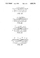
- FIG. 1 is a cross-sectional view of a beam lead mixer diode structure embodying the invention.
- FIG. 2A-2F are cross-sectional depictions of the structures resulting from steps of an exemplary process for fabricating a beam lead mixer diode embodying the invention.
- FIG. 1 A cross-sectional view of a planar beam lead mixer diode 10 employing a dielectric separator 28 in accordance with the invention is shown in FIG. 1.
- the diode comprises a substrate 12, comprising a semiinsulating Cr-doped Gallium Arsenide layer.
- a thin, heavily doped N + epitaxial layer 14 having a thickness of about 3 microns is grown on the top surface of the substrate 12.
- Conversion regions 16a and 16b whose lateral extents are defined by appropriate photolithographic masking techniques, are produced in the two layers 14 and 26 by a carefully controlled high energy proton bombardment of the structure. This bombardment damages the crystalline atomic structure of the N + and N layer regions, thereby converting the bombarded regions of the conductive N + layer region 14 and the N-doped layer 26 into nonconductive regions 16a and 16b, thereby defining the active diode region whose lateral extent is indicated by reference numeral 33.
- the depth of the N + layer 14 and the N layer 26 and the proton bombardment parameters are cooperatively selected to ensure that the protons penetrate to the bottom of the layer 14. Otherwise, a thin conductive layer would remain, creating a significant stray capacitance which would limit the frequency cut-off and bandwidth of the resulting diode.
- An ohmic contact 18 is formed in contact with region 14a of the N + layer 14 and the N layer 26.
- a thin dielectric separator 28 is fabricated on top of a portion of the conversion region 16b adjacent the active region 33, and preferably overlapping onto the active region 33 by one to two microns.
- the dielectric separator 28 is preferably of a thickness in the range of 0.2 to 2.0 microns.
- the Schottky contact comprises metallization layer 20 which is in turn formed on N layer 26.
- the metallization layer 20 is fabricated so as to extend over the separator 28 and over the portion of the conversion region 16b not covered by the dielectric separator 28.
- a gold beam lead 24 is plated to the top of the metallization layer 20.
- Another metallization layer 27 is formed over the ohmic contact 18 and the conversion region 16a.
- Another gold beam lead 22 is plated over the metallization layer 27. Electrical contact to the diode is made via the beam leads 22 and 24.
- the dielectric separator 28 is fabricated from a low permittivity material preferably having a permittivity less than six, such as silicon dioxide, and the thickness of the separator 28 serves to separate the metallization layer 20 from the conductive N + region 14.
- the separation distance coupled with the low permittivity of the separator 28 and the overlapping of the separator 28 over the active region substantially reduces the stray capitance between the highly conductive N + region 14 and the metallization layer 20. This capacitance is indicated by capacitance 30 in FIG. 1.
- the reduction in the stray capacitance achieved by the diode configuration of FIG. 1 results in a typical increase by a factor of 50 to 100 percent of the frequency bandwidth of the diode over conventional planar beam lead diodes fabricated with proton bombardment.
- This substantial improvement in the electrical performance is achieved without significant degradation of the mechanical stability of the diode, since the gold-plated beam lead 24 connected to the Schottky diode is still substantially supported by the proton bombarded conversion region 16b.
- the invention provides a diode having the electrical performance characteristics of the conventional mesa-type beam lead diode with dielectric beam supports, yet with the performance uniformity and mechanical stability of the conventional planar Schottky device.
- diodes embodying the invention may be fabricated by relatively low-cost, high-yield processes.
- FIGS. 2A-2F sequentially illustrate the structures (in cross-section) resulting from steps of an exemplary process for fabricating one beam lead mixer diode embodying the invention.
- FIG. 2A illustrates the basic epitaxial device structure.
- layer 12 is Cr-doped GaAs to form the semi-insulating substrate, typically about 250 microns in thickness.
- N + contact layer 14 is an epitaxial layer of GaAs with a concentration of 2 ⁇ 10 18 impurity ions per cubic centimeter, and a typical thickness of 2 to 3 microns.
- N layer 26 formed on layer 14 is an epitaxial layer of GaAs doped with a concentration of 10 17 impurity ions per cubic centimeter, and a thickness of 0.1 to 0.2 microns.
- FIGS. 2A-2F are not drawn to scale, and that the structure shown in these figures may be replicated throughout a GaAs wafer to form many diodes on the wafer in one sequence of processing steps. The diode structures may then be separted to form individual diodes.
- FIG. 2B illustrates the disposition of alloyed ohmic contact 18, which penetrates the N layer 26 to contact the conductive N + layer 14.
- the contact 18 may comprise an Au-Ge-Ni alloy, having a thickness of about 1.5 microns.
- FIG. 2C illustrates the conversion regions 16a and 16b formed in the layers 14 and 26 by proton bombardment.
- a suitable photoresist mask (not shown) protects the diode region generally indicated by reference numeral 33 against the bombardment, which employs protons with an energy level of about 400 KeV.
- the parameters of the bombardment are selected in cooperation with the thickness of layers 26 and 14 so that protons penetrate the entire thickness of layers 26 and 14.
- the conversion regions 16a and 16b border the diode active region whose lateral extent is indicated by reference numeral 33 in FIG. 2C.
- a dielectric separator 28 is formed on the surface of the conversion layer 16b.
- the dielectric separator preferably comprises silicon dioxide formed to a thickness of 2.0 microns.
- the lateral extent 29 of the separator 28 is defined in the conventional manner by an opening in a layer of photoresist (not shown) which has been selectively etched in the photoresist.
- a typical lateral dimension for the separator is 5 to 10 microns.
- the silicon dioxide separator 28 is formed by planar enhanced deposition or sputtering techniques. The resulting structure is shown in FIG. 2D.
- a Schottky metallization layer is applied to the structure to form layers 27 and 20.
- a gap 35 is formed between the metallization layers, and is typically about 15 microns in width.
- the gap is covered by a photoresist layer (not shown) during the metallization processing, and then removed to define the gap.
- the layer 27 is in electrical contact with the ohmic contact 18.
- the layer 20 forms a Schottky contact with the N layer 26, and is formed over the dielectric separator 28.
- Layers 27 and 20 have a typical thickness in the range of 4500 to 5000 Angstroms.
- gold beam leads 22 and 24 are plated over portions of the layers 27 and 20 with a typical thickness of 10 microns.
- the structure then undergoes a wafer thinning procedure, typically a back etch process, to reduce the thickness of the substrate 12 to about 1.5 mils and to reduce the lateral extent of the substrate 12 and conversion regions 16a and 16b.
- the various diode structures which have been replicated on the wafer may then be separated to form individual diode devices.
Abstract
Description
f.sub.co =(1/2 R.sub.s C.sub.o) (1)
Claims (12)
Priority Applications (1)
| Application Number | Priority Date | Filing Date | Title |
|---|---|---|---|
| US06/871,236 US4855796A (en) | 1986-06-06 | 1986-06-06 | Beam lead mixer diode |
Applications Claiming Priority (1)
| Application Number | Priority Date | Filing Date | Title |
|---|---|---|---|
| US06/871,236 US4855796A (en) | 1986-06-06 | 1986-06-06 | Beam lead mixer diode |
Publications (1)
| Publication Number | Publication Date |
|---|---|
| US4855796A true US4855796A (en) | 1989-08-08 |
Family
ID=25356996
Family Applications (1)
| Application Number | Title | Priority Date | Filing Date |
|---|---|---|---|
| US06/871,236 Expired - Lifetime US4855796A (en) | 1986-06-06 | 1986-06-06 | Beam lead mixer diode |
Country Status (1)
| Country | Link |
|---|---|
| US (1) | US4855796A (en) |
Cited By (9)
| Publication number | Priority date | Publication date | Assignee | Title |
|---|---|---|---|---|
| WO1990005997A1 (en) * | 1988-11-21 | 1990-05-31 | M-Pulse Microwave | An improved beam leads for schottky-barrier diodes in a ring quand |
| US5280194A (en) * | 1988-11-21 | 1994-01-18 | Micro Technology Partners | Electrical apparatus with a metallic layer coupled to a lower region of a substrate and metallic layer coupled to a lower region of a semiconductor device |
| US5403729A (en) * | 1992-05-27 | 1995-04-04 | Micro Technology Partners | Fabricating a semiconductor with an insulative coating |
| US5521420A (en) * | 1992-05-27 | 1996-05-28 | Micro Technology Partners | Fabricating a semiconductor with an insulative coating |
| US5557149A (en) * | 1994-05-11 | 1996-09-17 | Chipscale, Inc. | Semiconductor fabrication with contact processing for wrap-around flange interface |
| US5569886A (en) * | 1993-04-27 | 1996-10-29 | Matsushita Electric Industrial Co., Ltd. | Flexible printed circuit board |
| US5665999A (en) * | 1994-04-14 | 1997-09-09 | Daimler Benz Ag | Metal-semiconductor diode and process for preparing metal-semiconductor diodes |
| US6121119A (en) * | 1994-06-09 | 2000-09-19 | Chipscale, Inc. | Resistor fabrication |
| US20110089541A1 (en) * | 2009-10-19 | 2011-04-21 | Jeng-Jye Shau | Area reduction for electrical diode chips |
Citations (4)
| Publication number | Priority date | Publication date | Assignee | Title |
|---|---|---|---|---|
| US3836988A (en) * | 1972-11-24 | 1974-09-17 | Philips Corp | Semiconductor devices |
| US4301233A (en) * | 1980-05-29 | 1981-11-17 | Eaton Corporation | Beam lead Schottky barrier diode for operation at millimeter and submillimeter wave frequencies |
| US4499656A (en) * | 1983-08-15 | 1985-02-19 | Sperry Corporation | Deep mesa process for fabricating monolithic integrated Schottky barrier diode for millimeter wave mixers |
| US4577213A (en) * | 1984-03-05 | 1986-03-18 | Honeywell Inc. | Internally matched Schottky barrier beam lead diode |
-
1986
- 1986-06-06 US US06/871,236 patent/US4855796A/en not_active Expired - Lifetime
Patent Citations (4)
| Publication number | Priority date | Publication date | Assignee | Title |
|---|---|---|---|---|
| US3836988A (en) * | 1972-11-24 | 1974-09-17 | Philips Corp | Semiconductor devices |
| US4301233A (en) * | 1980-05-29 | 1981-11-17 | Eaton Corporation | Beam lead Schottky barrier diode for operation at millimeter and submillimeter wave frequencies |
| US4499656A (en) * | 1983-08-15 | 1985-02-19 | Sperry Corporation | Deep mesa process for fabricating monolithic integrated Schottky barrier diode for millimeter wave mixers |
| US4577213A (en) * | 1984-03-05 | 1986-03-18 | Honeywell Inc. | Internally matched Schottky barrier beam lead diode |
Non-Patent Citations (2)
| Title |
|---|
| Anderson et al., "GaAs Beam Lead Antiparallel Diodes for mm Wave Subharmonic Mixers", pp. 688-691, IEDM 81. |
| anderson et al., GaAs Beam Lead Antiparallel Diodes for mm Wave Subharmonic Mixers , pp. 688 691, IEDM 81. * |
Cited By (15)
| Publication number | Priority date | Publication date | Assignee | Title |
|---|---|---|---|---|
| US5455187A (en) * | 1988-11-21 | 1995-10-03 | Micro Technology Partners | Method of making a semiconductor device with a metallic layer coupled to a lower region of a substrate and metallic layer coupled to a lower region of a semiconductor device |
| US5280194A (en) * | 1988-11-21 | 1994-01-18 | Micro Technology Partners | Electrical apparatus with a metallic layer coupled to a lower region of a substrate and metallic layer coupled to a lower region of a semiconductor device |
| US5789817A (en) * | 1988-11-21 | 1998-08-04 | Chipscale, Inc. | Electrical apparatus with a metallic layer coupled to a lower region of a substrate and a metallic layer coupled to a lower region of a semiconductor device |
| WO1990005997A1 (en) * | 1988-11-21 | 1990-05-31 | M-Pulse Microwave | An improved beam leads for schottky-barrier diodes in a ring quand |
| US5521420A (en) * | 1992-05-27 | 1996-05-28 | Micro Technology Partners | Fabricating a semiconductor with an insulative coating |
| US5444009A (en) * | 1992-05-27 | 1995-08-22 | Micro Technology Partners | Fabricating a semiconductor with an insulative coating |
| US5441898A (en) * | 1992-05-27 | 1995-08-15 | Micro Technology Partners | Fabricating a semiconductor with an insulative coating |
| US5592022A (en) * | 1992-05-27 | 1997-01-07 | Chipscale, Inc. | Fabricating a semiconductor with an insulative coating |
| US5403729A (en) * | 1992-05-27 | 1995-04-04 | Micro Technology Partners | Fabricating a semiconductor with an insulative coating |
| US5569886A (en) * | 1993-04-27 | 1996-10-29 | Matsushita Electric Industrial Co., Ltd. | Flexible printed circuit board |
| US5665999A (en) * | 1994-04-14 | 1997-09-09 | Daimler Benz Ag | Metal-semiconductor diode and process for preparing metal-semiconductor diodes |
| US5557149A (en) * | 1994-05-11 | 1996-09-17 | Chipscale, Inc. | Semiconductor fabrication with contact processing for wrap-around flange interface |
| US5656547A (en) * | 1994-05-11 | 1997-08-12 | Chipscale, Inc. | Method for making a leadless surface mounted device with wrap-around flange interface contacts |
| US6121119A (en) * | 1994-06-09 | 2000-09-19 | Chipscale, Inc. | Resistor fabrication |
| US20110089541A1 (en) * | 2009-10-19 | 2011-04-21 | Jeng-Jye Shau | Area reduction for electrical diode chips |
Similar Documents
| Publication | Publication Date | Title |
|---|---|---|
| US4339870A (en) | Series-connected two-terminal semiconductor devices and their fabrication | |
| US5347149A (en) | Integrated circuit and method | |
| US5449930A (en) | High power, compound semiconductor device and fabrication process | |
| US5041881A (en) | Whiskerless Schottky diode | |
| US3967305A (en) | Multichannel junction field-effect transistor and process | |
| US4939562A (en) | Heterojunction bipolar transistors and method of manufacture | |
| US4141021A (en) | Field effect transistor having source and gate electrodes on opposite faces of active layer | |
| US20010023947A1 (en) | Ultra high speed heterojunction bipolar transistor having a cantilevered base | |
| US4924283A (en) | Heterojunction bipolar transistor and process for fabricating same | |
| US4855796A (en) | Beam lead mixer diode | |
| US4301233A (en) | Beam lead Schottky barrier diode for operation at millimeter and submillimeter wave frequencies | |
| US4127830A (en) | Microstrip switch wherein diodes are formed in single semiconductor body | |
| US4839709A (en) | Detector and mixer diode operative at zero bias voltage | |
| Irvin et al. | Fabrication and noise performance of high-power GaAs IMPATTS | |
| US4665413A (en) | Edge junction schottky diode | |
| JPS60133762A (en) | Field effect transistor of vertical structure | |
| US3416042A (en) | Microwave integrated circuit mixer | |
| US4674177A (en) | Method for making an edge junction schottky diode | |
| US4238763A (en) | Solid state microwave devices with small active contact and large passive contact | |
| EP0314712B1 (en) | Two-terminal semiconductor diode arrangement | |
| US4683642A (en) | Method for fabricating MOMS semiconductor device | |
| US3508125A (en) | Microwave mixer diode comprising a schottky barrier junction | |
| US5350702A (en) | Method for fabricating a dual-gate metal-semiconductor field effect transistor | |
| US4374392A (en) | Monolithic integrated circuit interconnection and fabrication method | |
| US4954864A (en) | Millimeter-wave monolithic diode-grid frequency multiplier |
Legal Events
| Date | Code | Title | Description |
|---|---|---|---|
| AS | Assignment |
Owner name: HUGHES AIRCRAFT COMPANY, LOS ANGELES, CALIFORNIA A Free format text: ASSIGNMENT OF ASSIGNORS INTEREST.;ASSIGNORS:WONG, WAH S.;WEN, CHENG P.;KUNG, JEN K.;REEL/FRAME:004568/0001 Effective date: 19860530 |
|
| STCF | Information on status: patent grant |
Free format text: PATENTED CASE |
|
| FPAY | Fee payment |
Year of fee payment: 4 |
|
| FEPP | Fee payment procedure |
Free format text: PAYOR NUMBER ASSIGNED (ORIGINAL EVENT CODE: ASPN); ENTITY STATUS OF PATENT OWNER: LARGE ENTITY |
|
| FPAY | Fee payment |
Year of fee payment: 8 |
|
| FPAY | Fee payment |
Year of fee payment: 12 |
|
| AS | Assignment |
Owner name: HE HOLDINGS, INC., A DELAWARE CORP., CALIFORNIA Free format text: CHANGE OF NAME;ASSIGNOR:HUGHES AIRCRAFT COMPANY, A CORPORATION OF THE STATE OF DELAWARE;REEL/FRAME:016087/0541 Effective date: 19971217 Owner name: RAYTHEON COMPANY, MASSACHUSETTS Free format text: MERGER;ASSIGNOR:HE HOLDINGS, INC. DBA HUGHES ELECTRONICS;REEL/FRAME:016116/0506 Effective date: 19971217 |