US4875134A - Pressure sensor construction and method for its fabrication - Google Patents
Pressure sensor construction and method for its fabrication Download PDFInfo
- Publication number
- US4875134A US4875134A US07/294,799 US29479989A US4875134A US 4875134 A US4875134 A US 4875134A US 29479989 A US29479989 A US 29479989A US 4875134 A US4875134 A US 4875134A
- Authority
- US
- United States
- Prior art keywords
- electrode
- base part
- capacitor electrode
- silicon
- pressure sensor
- Prior art date
- Legal status (The legal status is an assumption and is not a legal conclusion. Google has not performed a legal analysis and makes no representation as to the accuracy of the status listed.)
- Expired - Lifetime
Links
Images


Classifications
-
- G—PHYSICS
- G01—MEASURING; TESTING
- G01L—MEASURING FORCE, STRESS, TORQUE, WORK, MECHANICAL POWER, MECHANICAL EFFICIENCY, OR FLUID PRESSURE
- G01L9/00—Measuring steady of quasi-steady pressure of fluid or fluent solid material by electric or magnetic pressure-sensitive elements; Transmitting or indicating the displacement of mechanical pressure-sensitive elements, used to measure the steady or quasi-steady pressure of a fluid or fluent solid material, by electric or magnetic means
- G01L9/0041—Transmitting or indicating the displacement of flexible diaphragms
- G01L9/0072—Transmitting or indicating the displacement of flexible diaphragms using variations in capacitance
- G01L9/0073—Transmitting or indicating the displacement of flexible diaphragms using variations in capacitance using a semiconductive diaphragm
-
- Y—GENERAL TAGGING OF NEW TECHNOLOGICAL DEVELOPMENTS; GENERAL TAGGING OF CROSS-SECTIONAL TECHNOLOGIES SPANNING OVER SEVERAL SECTIONS OF THE IPC; TECHNICAL SUBJECTS COVERED BY FORMER USPC CROSS-REFERENCE ART COLLECTIONS [XRACs] AND DIGESTS
- Y10—TECHNICAL SUBJECTS COVERED BY FORMER USPC
- Y10T—TECHNICAL SUBJECTS COVERED BY FORMER US CLASSIFICATION
- Y10T29/00—Metal working
- Y10T29/43—Electric condenser making
- Y10T29/435—Solid dielectric type
Definitions
- the present invention relates to a pressure sensor construction which includes a fixed planar capacitor and a deflecting membrane capacitor.
- the invention also concerns a method for producing said pressure sensor construction.
- U.S. patent publication No. 4 597 027 and U.S. patent publication No. 4 609 966 is a capacitive pressure sensor construction with silicon/glass structure, in which construction the silicon element with its center area thinned into a membrane is attached by anodic bonding to a glass layer deposited on top a second silicon element so that there remains a shallow, hermetically closed, gapped space between these two parts.
- the fixed planar capacitor electrode which is placed on the glass layer in the gapped space, is electrically contacted to the second silicon element.
- the thinned silicon membrane serves as the other, pressure-deflected capacitor electrode.
- a stray capacitance is formed across the glass layer at the areas bonding the elements, which capacitance is effectively coupled in parallel with the measured sensor capacitance.
- a voltage of several hundreds of volts is applied in the anodic bonding process between the silicon elements.
- the same voltage is also effective over all capacitors of sensor items contained on the silicon wafer. Because the width of the dielectric gap is only in the order of a few micrometers, there is a high probability of electrical break-through. Thence, extremely high cleanliness and smoothness is required from all surfaces in the process.
- the aim of the present invention is to overcome the disadvantages of the prior art technology and achieve a totally new kind of pressure sensor construction and method for fabricating the sensor.
- the invention is based on dividing the silicon wafer acting at the sensor substrate into galvanically isolated subareas so that each fixed electrode of the sensor capacitor is provided with a dedicated contact area, galvanically connected to the capacitor electrode and surrounded by a bonding area, the contact area being galvanically isolated from the bonding area to which a high bonding voltage is applicable during the anodic bonding process.
- the pressure sensor in accordance with the invention is characterized by what is stated in the characterizing part of claim 1.
- the invention provides outstanding benefits.
- the construction according to the invention avoids stray capacitances at the bonding areas, because the contact area of the substrate can be designed small. Further, the high voltage required in anodic bonding can be decoupled from the capacitor dielectric gap by arranging a galvanic isolation between the bonding area of the substrate and the capacitor area. Furthermore, electrical bonding to the sensor electrodes is also feasible at the lower side of the sensor construction.
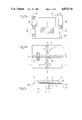
- FIG. 1a is a sectional side view of a sensor construction in accordance with the invention.
- FIG. 1b is a sectional view taken along plane A--A of the sensor construction illustrated in FIG. 1a.
- FIG. 2 is a bottom view of a second sensor construction in accordance with the invention.
- FIG. 3a is a partially sectioned top view of a third sensor construction in accordance with the invention.
- FIG. 3b is a bottom view of the sensor construction illustrated in FIG. 3a.
- FIG. 3c is a sectional view taken along plane B--B of the sensor construction illustrated in FIG. 3a.
- FIG. 4a is a bottom view of a fourth sensor construction in accordance with the invention.
- FIG. 4b is a sectional view taken along plane C--C of the sensor construction illustrated in FIG. 4a.
- FIG. 5 shows a production stage of the sensor construction in accordance with the invention.
- FIG. 6 shows a production stage of the second sensor construction in accordance with the invention.
- FIGS. 1a and 1b show a feasible embodiment of the sensor construction.
- the construction has a silicon base part 1, 2 divided with a tubular glass isolator 3 into two sections, namely a bonding section 1 and a cylindrical contact section 2.
- the top side of the sections 1 and 2 is covered by a glass layer 4.
- the contact section 2 communicates with a fixed planar capacitor electrode 9, which is deposited on the glass isolation layer 4, via a silicon bump 10.
- Anodic bonding is made to the glass layer 4 where the glass layer 4 meets the bonding section 1.
- the sensor capacitance is measured between the contact section 2 and a silicon base element 5.
- the bonding section 1 is connected to ground potential, whereby the use of a suitable measurement configuration eliminates the effect of stray capacitance formed across the glass layer 4.
- the voltage required in the anodic bonding process of sensor fabrication is applied between the bonding section 1 and the body element 5, thus being effectively decoupled from the dielectric gap between the capacitor electrodes 6 and 9.
- the glass pattern 3 isolating the sections 1 and 2 may be shaped into the form of perpendicularly intersecting strips as illustrated in FIG. 2, or into an alternative shape.
- the contact section 2 becomes the shape of a parallelepiped.
- the choice of an insulator pattern is mainly determined by fabrication method used. Variations in the area of the bare silicon section 2 are also feasible.
- FIGS. 3a-3c A third feasible embodiment of the sensor construction is illustrated in detail in FIGS. 3a-3c.
- the silicon area 2 acting as the contact area is a column, which is surrounded by elongated vertical glass layers 3 and is electrically communicating with a fixed planar capacitor electrode 9.
- the glass layers additionally border eight other silicon areas 1, 16, and 16'.
- the silicon area 16 is connected to the silicon area 2 via a metallized thin-film conductor 13 fabricated on the lower surface of the sensor.
- the other silicon areas are correspondingly connected to each other by metallic conductor patterns 12. Electrical contacts are routed through the glass layer 4 to the upper surface of the sensor by means of silicon bumps 26.
- the metallized area 11 is grounded, and the sensor capacitance is measured across metallized areas 17 and 18.
- FIGS. 4a and 4b Shown in FIGS. 4a and 4b is a sensor construction, in which the contact areas are routed to the lower surface of the sensor.
- FIG. 4b shows an upside down inverted sectional view taken along plane C--C of the sensor construction illustrated in FIG. 4a.
- the illustrated embodiment utilizes another insulated silicon area 20, which communicates electrically via a silicon bump 21 extending through the glass layer 4, with a silicon element 5 and further with a silicon membrane 6, which provides for the second capacitor electrode.
- the lower side of the sensor is provided with thin-film metallized areas 22, 23, and 24, on which conductor bonding is made by soldering, welding or a similar method.
- the area 22 is connected to the silicon area 2, area 23 to the silicon area 20, and area 24 to the rest of the silicon areas.
- the sensor capacitance is measurable across the areas 22 and 23 when the areas 24 are connected to ground potential in the measurement configuration.
- the thickness of the glass layer 3 may be 10-500 ⁇ m, preferably 150 ⁇ m.
- the thickness of the glass layer may be 1-150 ⁇ m, preferably 30 ⁇ m.
- the structure illustrated in the examples can be fabricated according to FIG. 5 as follows:
- the silicon surface is etched or otherwise processed to obtain silicon bumps 10, which are required to extend through the glass layer 4;
- the silicon wafer is processed for deep, narrow grooves 3 with a sufficient depth to nearly separate the silicon areas from each other.
- the areas remain connected to each other by isthmuses 19 at the bottom of the silicon wafer.
- the shape and dimensions of the areas and grooves are determined by the processing method used for fabricating the grooves 3.
- Applicable methods are, e.g., drilling with a hollow drill, etching, laser machining, spark erosion and sawing. Among the mentioned methods, the three latter are especially viable. Sawing effortlessly produces narrow grooves, which, however, divide the wafer into unnecessary many chips. On the other hand, laser machining requires accurate depth control;
- glass powder 7 is spread over the silicon surface and melted until the glass fills the grooves;
- the glass surface is honed down to a level, e.g., marked approximately as level D, so as to expose the silicon bumps but yet retaining a glass layer 4 of desired thickness on the other areas;
- silicon is honed away from the lower side of the wafer down to a level, e.g., marked approximately as level E, until the isthmus 19 is removed and the silicon chips are separated from each other;
- the glass surface is polished.
- the described construction and method is readily developed into several variations. Characteristic to the method is that a single wafer of the base material is processed into a wafer containing several parts isolated from each other. The fabrication method is characterized by the nearly completed separation of the chips on the wafer from each other, a subsequent glass melting phase, and a final separation of the chips from the wafer. This approach maintains the planar shape of the base material wafer and the dimensional accuracy of the elements. Alternatively, a feasible approach is to mount the base material wafer rigidly to another support wafer 27 in accordance with FIG. 6 so that the grooves may be machined entirely penetrating the base material wafer. After the melting and glass honing phases, the support wafer is detached.
- the mutually isolated elements of the sensor chip can be used as feedthrough elements in a variety.
- the sensor construction illustrated in FIGS. 3a-3c gives an example of this possibility.
Abstract
Description
Claims (8)
Applications Claiming Priority (2)
| Application Number | Priority Date | Filing Date | Title |
|---|---|---|---|
| FI880206A FI78784C (en) | 1988-01-18 | 1988-01-18 | TRYCKGIVARKONSTRUKTION OCH FOERFARANDE FOER FRAMSTAELLNING DAERAV. |
| FI880206 | 1988-01-18 |
Publications (1)
| Publication Number | Publication Date |
|---|---|
| US4875134A true US4875134A (en) | 1989-10-17 |
Family
ID=8525738
Family Applications (1)
| Application Number | Title | Priority Date | Filing Date |
|---|---|---|---|
| US07/294,799 Expired - Lifetime US4875134A (en) | 1988-01-18 | 1989-01-09 | Pressure sensor construction and method for its fabrication |
Country Status (6)
| Country | Link |
|---|---|
| US (1) | US4875134A (en) |
| JP (1) | JP2574443B2 (en) |
| DE (1) | DE3900654C2 (en) |
| FI (1) | FI78784C (en) |
| FR (1) | FR2626073B1 (en) |
| GB (1) | GB2214350B (en) |
Cited By (21)
| Publication number | Priority date | Publication date | Assignee | Title |
|---|---|---|---|---|
| US4935841A (en) * | 1987-02-12 | 1990-06-19 | Johnsson & Billquist Development Ab | Pressure sensor |
| US5165281A (en) * | 1989-09-22 | 1992-11-24 | Bell Robert L | High pressure capacitive transducer |
| US5173836A (en) * | 1992-03-05 | 1992-12-22 | Motorola, Inc. | Hermetically sealed interface |
| US5249469A (en) * | 1988-05-17 | 1993-10-05 | Jonsson & Billquist Development Ab | Pressure gauge |
| US5285097A (en) * | 1991-02-25 | 1994-02-08 | Canon Kabushiki Kaisha | Semiconductor sensor of electrostatic capacitance type |
| US5365790A (en) * | 1992-04-02 | 1994-11-22 | Motorola, Inc. | Device with bonded conductive and insulating substrates and method therefore |
| US5418681A (en) * | 1992-02-20 | 1995-05-23 | Sextant Avionique | Capacitive micro-sensor with a lateral protection and manufacturing method |
| WO1996016418A1 (en) * | 1994-11-22 | 1996-05-30 | Case Western Reserve University | Capacitive absolute pressure sensor and method |
| US5673476A (en) * | 1992-10-22 | 1997-10-07 | Canon Kabushiki Kaisha | Anode bonding method for selected regions |
| US5744725A (en) * | 1994-04-18 | 1998-04-28 | Motorola Inc. | Capacitive pressure sensor and method of fabricating same |
| US20050023629A1 (en) * | 2003-07-31 | 2005-02-03 | Xiaoyi Ding | Wafer-level sealed microdevice having trench isolation and methods for making the same |
| EP1612533A1 (en) * | 2004-07-02 | 2006-01-04 | Alps Electric Co., Ltd. | Glass substrate and capacitance-type pressure sensor using the same |
| EP1681545A2 (en) * | 2004-12-17 | 2006-07-19 | Alps Electric Co., Ltd. | Capacitive pressure sensor |
| EP1780525A1 (en) * | 2005-10-31 | 2007-05-02 | Alps Electric Co., Ltd. | Capacitive pressure sensor |
| EP2067391A1 (en) * | 2006-09-04 | 2009-06-10 | NanoSpace AB | Substrate-penetrating electrical connections |
| EP1371092B2 (en) † | 2001-03-14 | 2010-11-03 | Fraunhofer-Gesellschaft zur Förderung der angewandten Forschung e.V. | Method for structuring a flat substrate consisting of a glass-type material |
| EP2377809A1 (en) * | 2010-04-16 | 2011-10-19 | SensoNor Technologies AS | Method for Manufacturing a Hermetically Sealed Structure |
| EP2508860A2 (en) | 2011-03-31 | 2012-10-10 | Codman Neuro Sciences Sàrl | Monitoring and recording implantable silicon active pressure transducer |
| CN101449347B (en) * | 2006-04-13 | 2013-07-17 | 三星电子株式会社 | Capacitive micro- electro-mechanical sensors with single crystal silicon electrodes |
| US8590387B2 (en) | 2011-03-31 | 2013-11-26 | DePuy Synthes Products, LLC | Absolute capacitive micro pressure sensor |
| US9249008B2 (en) | 2012-12-20 | 2016-02-02 | Industrial Technology Research Institute | MEMS device with multiple electrodes and fabricating method thereof |
Families Citing this family (5)
| Publication number | Priority date | Publication date | Assignee | Title |
|---|---|---|---|---|
| FI893874A (en) * | 1989-08-17 | 1991-02-18 | Vaisala Oy | KONTAKTFOERSEDD GIVARE MED SKIKTSTRUKTUR SAMT FOERFARANDE FOER UTFOERANDE AV KONTAKTERINGEN. |
| DE3937529A1 (en) * | 1989-11-08 | 1991-05-16 | Siemens Ag | METHOD FOR CONNECTING A SILICON PART TO A GLASS PART |
| DE4006108A1 (en) * | 1990-02-27 | 1991-08-29 | Bosch Gmbh Robert | METHOD FOR BUILDING MICROMECHANICAL COMPONENTS IN THICK LAYER TECHNOLOGY |
| DE4311762C2 (en) * | 1993-04-08 | 1995-02-02 | Josef Dr Kemmer | Method of connecting electrical contact points |
| JP2007085837A (en) * | 2005-09-21 | 2007-04-05 | Alps Electric Co Ltd | Capacitance type pressure sensor |
Citations (7)
| Publication number | Priority date | Publication date | Assignee | Title |
|---|---|---|---|---|
| US4495820A (en) * | 1981-09-30 | 1985-01-29 | Hitachi, Ltd. | Capacitive pressure sensor |
| US4594639A (en) * | 1984-02-21 | 1986-06-10 | Vaisala Oy | Capacitive pressure detector |
| US4597027A (en) * | 1984-06-07 | 1986-06-24 | Vaisala Oy | Capacitive pressure detector structure and method for manufacturing same |
| US4609966A (en) * | 1984-10-11 | 1986-09-02 | Vaisala Oy | Absolute pressure transducer |
| US4625561A (en) * | 1984-12-06 | 1986-12-02 | Ford Motor Company | Silicon capacitive pressure sensor and method of making |
| US4730496A (en) * | 1986-06-23 | 1988-03-15 | Rosemount Inc. | Capacitance pressure sensor |
| US4773972A (en) * | 1986-10-30 | 1988-09-27 | Ford Motor Company | Method of making silicon capacitive pressure sensor with glass layer between silicon wafers |
Family Cites Families (2)
| Publication number | Priority date | Publication date | Assignee | Title |
|---|---|---|---|---|
| JPS5516228A (en) * | 1978-07-21 | 1980-02-04 | Hitachi Ltd | Capacity type sensor |
| US4701826A (en) * | 1986-10-30 | 1987-10-20 | Ford Motor Company | High temperature pressure sensor with low parasitic capacitance |
-
1988
- 1988-01-18 FI FI880206A patent/FI78784C/en not_active IP Right Cessation
-
1989
- 1989-01-06 GB GB8900235A patent/GB2214350B/en not_active Expired - Lifetime
- 1989-01-09 US US07/294,799 patent/US4875134A/en not_active Expired - Lifetime
- 1989-01-11 DE DE3900654A patent/DE3900654C2/en not_active Expired - Lifetime
- 1989-01-13 FR FR8900383A patent/FR2626073B1/en not_active Expired - Lifetime
- 1989-01-18 JP JP1009626A patent/JP2574443B2/en not_active Expired - Lifetime
Patent Citations (7)
| Publication number | Priority date | Publication date | Assignee | Title |
|---|---|---|---|---|
| US4495820A (en) * | 1981-09-30 | 1985-01-29 | Hitachi, Ltd. | Capacitive pressure sensor |
| US4594639A (en) * | 1984-02-21 | 1986-06-10 | Vaisala Oy | Capacitive pressure detector |
| US4597027A (en) * | 1984-06-07 | 1986-06-24 | Vaisala Oy | Capacitive pressure detector structure and method for manufacturing same |
| US4609966A (en) * | 1984-10-11 | 1986-09-02 | Vaisala Oy | Absolute pressure transducer |
| US4625561A (en) * | 1984-12-06 | 1986-12-02 | Ford Motor Company | Silicon capacitive pressure sensor and method of making |
| US4730496A (en) * | 1986-06-23 | 1988-03-15 | Rosemount Inc. | Capacitance pressure sensor |
| US4773972A (en) * | 1986-10-30 | 1988-09-27 | Ford Motor Company | Method of making silicon capacitive pressure sensor with glass layer between silicon wafers |
Cited By (40)
| Publication number | Priority date | Publication date | Assignee | Title |
|---|---|---|---|---|
| US4935841A (en) * | 1987-02-12 | 1990-06-19 | Johnsson & Billquist Development Ab | Pressure sensor |
| US5249469A (en) * | 1988-05-17 | 1993-10-05 | Jonsson & Billquist Development Ab | Pressure gauge |
| US5165281A (en) * | 1989-09-22 | 1992-11-24 | Bell Robert L | High pressure capacitive transducer |
| US5285097A (en) * | 1991-02-25 | 1994-02-08 | Canon Kabushiki Kaisha | Semiconductor sensor of electrostatic capacitance type |
| US5418681A (en) * | 1992-02-20 | 1995-05-23 | Sextant Avionique | Capacitive micro-sensor with a lateral protection and manufacturing method |
| US5173836A (en) * | 1992-03-05 | 1992-12-22 | Motorola, Inc. | Hermetically sealed interface |
| US5365790A (en) * | 1992-04-02 | 1994-11-22 | Motorola, Inc. | Device with bonded conductive and insulating substrates and method therefore |
| US5673476A (en) * | 1992-10-22 | 1997-10-07 | Canon Kabushiki Kaisha | Anode bonding method for selected regions |
| US5744725A (en) * | 1994-04-18 | 1998-04-28 | Motorola Inc. | Capacitive pressure sensor and method of fabricating same |
| US5585311A (en) * | 1994-11-22 | 1996-12-17 | Case Western Reserve University | Capacitive absolute pressure sensor and method |
| WO1996016418A1 (en) * | 1994-11-22 | 1996-05-30 | Case Western Reserve University | Capacitive absolute pressure sensor and method |
| CN1092836C (en) * | 1994-11-22 | 2002-10-16 | 卡斯西部储备大学 | Capacitive absolute pressure sensor and method for making |
| EP1371092B2 (en) † | 2001-03-14 | 2010-11-03 | Fraunhofer-Gesellschaft zur Förderung der angewandten Forschung e.V. | Method for structuring a flat substrate consisting of a glass-type material |
| US20050023629A1 (en) * | 2003-07-31 | 2005-02-03 | Xiaoyi Ding | Wafer-level sealed microdevice having trench isolation and methods for making the same |
| US7378294B2 (en) | 2003-07-31 | 2008-05-27 | Temic Automotive Of North America, Inc. | Wafer-level sealed microdevice having trench isolation and methods for making the same |
| US7045868B2 (en) | 2003-07-31 | 2006-05-16 | Motorola, Inc. | Wafer-level sealed microdevice having trench isolation and methods for making the same |
| US20060105503A1 (en) * | 2003-07-31 | 2006-05-18 | Xiaoyi Ding | Wafer-level sealed microdevice having trench isolation and methods for making the same |
| US20070264742A1 (en) * | 2004-07-02 | 2007-11-15 | Alps Electric Co., Ltd. | Glass substrate and capacitance-type pressure sensor using the same |
| US20060001128A1 (en) * | 2004-07-02 | 2006-01-05 | Alps Electric Co., Ltd. | Glass substrate and capacitance-type pressure sensor using the same |
| US7535096B2 (en) * | 2004-07-02 | 2009-05-19 | Alps Electric Co., Ltd. | Glass substrate and capacitance-type pressure sensor using the same |
| EP1612533A1 (en) * | 2004-07-02 | 2006-01-04 | Alps Electric Co., Ltd. | Glass substrate and capacitance-type pressure sensor using the same |
| EP1681545A2 (en) * | 2004-12-17 | 2006-07-19 | Alps Electric Co., Ltd. | Capacitive pressure sensor |
| EP1681545A3 (en) * | 2004-12-17 | 2007-12-05 | Alps Electric Co., Ltd. | Capacitive pressure sensor |
| US20070095147A1 (en) * | 2005-10-31 | 2007-05-03 | Alps Electric Co., Ltd. | Capacitive pressure sensor |
| US7382599B2 (en) | 2005-10-31 | 2008-06-03 | Alps Electric Co., Ltd | Capacitive pressure sensor |
| EP1780525A1 (en) * | 2005-10-31 | 2007-05-02 | Alps Electric Co., Ltd. | Capacitive pressure sensor |
| CN101449347B (en) * | 2006-04-13 | 2013-07-17 | 三星电子株式会社 | Capacitive micro- electro-mechanical sensors with single crystal silicon electrodes |
| EP2067391A1 (en) * | 2006-09-04 | 2009-06-10 | NanoSpace AB | Substrate-penetrating electrical connections |
| EP2067391A4 (en) * | 2006-09-04 | 2014-05-07 | Nanospace Ab | Substrate-penetrating electrical connections |
| WO2011128446A2 (en) | 2010-04-16 | 2011-10-20 | Sensonor Technologies As | Method for manufacturing a hermetically sealed structure |
| CN102947217A (en) * | 2010-04-16 | 2013-02-27 | 森松诺尔有限公司 | Method for manufacturing hermetically sealed structure |
| WO2011128446A3 (en) * | 2010-04-16 | 2012-02-16 | Sensonor Technologies As | Method for manufacturing a hermetically sealed structure |
| EP2377809A1 (en) * | 2010-04-16 | 2011-10-19 | SensoNor Technologies AS | Method for Manufacturing a Hermetically Sealed Structure |
| US9051172B2 (en) | 2010-04-16 | 2015-06-09 | Sensonor As | Method for manufacturing a hermetically sealed structure |
| RU2568947C2 (en) * | 2010-04-16 | 2015-11-20 | Сенсонор Ас | Method of making sealed structure |
| EP2508860A2 (en) | 2011-03-31 | 2012-10-10 | Codman Neuro Sciences Sàrl | Monitoring and recording implantable silicon active pressure transducer |
| US8578795B2 (en) | 2011-03-31 | 2013-11-12 | DePuy Synthes Products, LLC | Monitoring and recording implantable silicon active pressure transducer |
| US8590387B2 (en) | 2011-03-31 | 2013-11-26 | DePuy Synthes Products, LLC | Absolute capacitive micro pressure sensor |
| EP3073239A1 (en) | 2011-03-31 | 2016-09-28 | Codman Neuro Sciences Sàrl | Monitoring and recording implantable silicon active pressure transducer |
| US9249008B2 (en) | 2012-12-20 | 2016-02-02 | Industrial Technology Research Institute | MEMS device with multiple electrodes and fabricating method thereof |
Also Published As
| Publication number | Publication date |
|---|---|
| FR2626073A1 (en) | 1989-07-21 |
| GB2214350B (en) | 1991-06-05 |
| DE3900654C2 (en) | 1997-05-22 |
| FR2626073B1 (en) | 1993-09-10 |
| JPH01288747A (en) | 1989-11-21 |
| FI78784B (en) | 1989-05-31 |
| GB8900235D0 (en) | 1989-03-08 |
| JP2574443B2 (en) | 1997-01-22 |
| FI880206A0 (en) | 1988-01-18 |
| FI78784C (en) | 1989-09-11 |
| DE3900654A1 (en) | 1989-07-27 |
| GB2214350A (en) | 1989-08-31 |
Similar Documents
| Publication | Publication Date | Title |
|---|---|---|
| US4875134A (en) | Pressure sensor construction and method for its fabrication | |
| US5559290A (en) | Capacitance type accelerometer | |
| KR910010061B1 (en) | A method for manufacturing semiconductor absolute pressure sensor units | |
| US5905203A (en) | Micromechanical acceleration sensor | |
| US8025625B2 (en) | Sensor with electromagnetically coupled hermetic pressure reference | |
| US4384899A (en) | Bonding method adaptable for manufacturing capacitive pressure sensing elements | |
| US7539003B2 (en) | Capacitive micro-electro-mechanical sensors with single crystal silicon electrodes | |
| EP0252929B1 (en) | Electrically variable piezoelectric hybrid capacitor | |
| US20040016989A1 (en) | MEMS device integrated chip package, and method of making same | |
| US20070199385A1 (en) | Capacitor electrode formed on surface of integrated circuit chip | |
| US4908921A (en) | Method of making capacitive pressure sensors | |
| GB2165652A (en) | Capacitive fluid pressure sensors | |
| JPH08264810A (en) | Micromechanism semiconductor device and its preparation | |
| CA2116382A1 (en) | Micromechanical Accelerometer and Method for the Production Thereof | |
| US5840597A (en) | Method of making a semiconductor device force and/or acceleration sensor | |
| KR20000005837A (en) | Chip-type piezoelectric resonator and method for adjusting resonance frequency thereof | |
| CN108362408B (en) | Pressure sensor and method for manufacturing the same | |
| FR2622975A1 (en) | CAPACITIVE ACCELEROMETER AND METHOD FOR MANUFACTURING THE SAME | |
| US7285844B2 (en) | Multiple internal seal right micro-electro-mechanical system vacuum package | |
| US4597027A (en) | Capacitive pressure detector structure and method for manufacturing same | |
| US5245504A (en) | Methodology for manufacturing hinged diaphragms for semiconductor sensors | |
| JP4539413B2 (en) | Structure of capacitive sensor | |
| JP2728237B2 (en) | Capacitive acceleration sensor | |
| KR20040097952A (en) | Capacitance type dynamic quantity sensor | |
| JPH10177034A (en) | Capacitance type acceleration sensor and its manufacture |
Legal Events
| Date | Code | Title | Description |
|---|---|---|---|
| AS | Assignment |
Owner name: VAISALA OY, FINLAND Free format text: ASSIGNMENT OF ASSIGNORS INTEREST.;ASSIGNOR:KUISMA, HEIKKI;REEL/FRAME:005017/0609 Effective date: 19881216 |
|
| STCF | Information on status: patent grant |
Free format text: PATENTED CASE |
|
| FEPP | Fee payment procedure |
Free format text: PAYOR NUMBER ASSIGNED (ORIGINAL EVENT CODE: ASPN); ENTITY STATUS OF PATENT OWNER: LARGE ENTITY |
|
| FEPP | Fee payment procedure |
Free format text: PAYER NUMBER DE-ASSIGNED (ORIGINAL EVENT CODE: RMPN); ENTITY STATUS OF PATENT OWNER: LARGE ENTITY Free format text: PAYOR NUMBER ASSIGNED (ORIGINAL EVENT CODE: ASPN); ENTITY STATUS OF PATENT OWNER: LARGE ENTITY |
|
| FPAY | Fee payment |
Year of fee payment: 4 |
|
| AS | Assignment |
Owner name: BREED AUTOMOTIVE TECHNOLOGY, INC., FLORIDA Free format text: MEMORANDUM OF LICENSE AGREEMENT;ASSIGNOR:VAISALA OY;REEL/FRAME:008153/0211 Effective date: 19960521 |
|
| FPAY | Fee payment |
Year of fee payment: 8 |
|
| FPAY | Fee payment |
Year of fee payment: 12 |