US4900279A - Solder terminal - Google Patents
Solder terminal Download PDFInfo
- Publication number
- US4900279A US4900279A US07/342,102 US34210289A US4900279A US 4900279 A US4900279 A US 4900279A US 34210289 A US34210289 A US 34210289A US 4900279 A US4900279 A US 4900279A
- Authority
- US
- United States
- Prior art keywords
- solder
- contact
- arm
- terminal
- bridge
- Prior art date
- Legal status (The legal status is an assumption and is not a legal conclusion. Google has not performed a legal analysis and makes no representation as to the accuracy of the status listed.)
- Expired - Lifetime
Links
Images
Classifications
-
- H—ELECTRICITY
- H01—ELECTRIC ELEMENTS
- H01R—ELECTRICALLY-CONDUCTIVE CONNECTIONS; STRUCTURAL ASSOCIATIONS OF A PLURALITY OF MUTUALLY-INSULATED ELECTRICAL CONNECTING ELEMENTS; COUPLING DEVICES; CURRENT COLLECTORS
- H01R12/00—Structural associations of a plurality of mutually-insulated electrical connecting elements, specially adapted for printed circuits, e.g. printed circuit boards [PCB], flat or ribbon cables, or like generally planar structures, e.g. terminal strips, terminal blocks; Coupling devices specially adapted for printed circuits, flat or ribbon cables, or like generally planar structures; Terminals specially adapted for contact with, or insertion into, printed circuits, flat or ribbon cables, or like generally planar structures
- H01R12/50—Fixed connections
- H01R12/51—Fixed connections for rigid printed circuits or like structures
- H01R12/55—Fixed connections for rigid printed circuits or like structures characterised by the terminals
- H01R12/57—Fixed connections for rigid printed circuits or like structures characterised by the terminals surface mounting terminals
-
- H—ELECTRICITY
- H05—ELECTRIC TECHNIQUES NOT OTHERWISE PROVIDED FOR
- H05K—PRINTED CIRCUITS; CASINGS OR CONSTRUCTIONAL DETAILS OF ELECTRIC APPARATUS; MANUFACTURE OF ASSEMBLAGES OF ELECTRICAL COMPONENTS
- H05K3/00—Apparatus or processes for manufacturing printed circuits
- H05K3/30—Assembling printed circuits with electric components, e.g. with resistor
- H05K3/32—Assembling printed circuits with electric components, e.g. with resistor electrically connecting electric components or wires to printed circuits
- H05K3/34—Assembling printed circuits with electric components, e.g. with resistor electrically connecting electric components or wires to printed circuits by soldering
- H05K3/3405—Edge mounted components, e.g. terminals
-
- H—ELECTRICITY
- H01—ELECTRIC ELEMENTS
- H01R—ELECTRICALLY-CONDUCTIVE CONNECTIONS; STRUCTURAL ASSOCIATIONS OF A PLURALITY OF MUTUALLY-INSULATED ELECTRICAL CONNECTING ELEMENTS; COUPLING DEVICES; CURRENT COLLECTORS
- H01R4/00—Electrically-conductive connections between two or more conductive members in direct contact, i.e. touching one another; Means for effecting or maintaining such contact; Electrically-conductive connections having two or more spaced connecting locations for conductors and using contact members penetrating insulation
- H01R4/02—Soldered or welded connections
-
- H—ELECTRICITY
- H05—ELECTRIC TECHNIQUES NOT OTHERWISE PROVIDED FOR
- H05K—PRINTED CIRCUITS; CASINGS OR CONSTRUCTIONAL DETAILS OF ELECTRIC APPARATUS; MANUFACTURE OF ASSEMBLAGES OF ELECTRICAL COMPONENTS
- H05K2201/00—Indexing scheme relating to printed circuits covered by H05K1/00
- H05K2201/10—Details of components or other objects attached to or integrated in a printed circuit board
- H05K2201/10227—Other objects, e.g. metallic pieces
- H05K2201/10386—Clip leads; Terminals gripping the edge of a substrate
-
- H—ELECTRICITY
- H05—ELECTRIC TECHNIQUES NOT OTHERWISE PROVIDED FOR
- H05K—PRINTED CIRCUITS; CASINGS OR CONSTRUCTIONAL DETAILS OF ELECTRIC APPARATUS; MANUFACTURE OF ASSEMBLAGES OF ELECTRICAL COMPONENTS
- H05K2201/00—Indexing scheme relating to printed circuits covered by H05K1/00
- H05K2201/10—Details of components or other objects attached to or integrated in a printed circuit board
- H05K2201/10613—Details of electrical connections of non-printed components, e.g. special leads
- H05K2201/10954—Other details of electrical connections
- H05K2201/10984—Component carrying a connection agent, e.g. solder, adhesive
Definitions
- the invention relates to solder terminals, particularly solder clips for forming soldered connections with contact pads on the edges of substrates.
- solder terminals include clips for mounting on the edges of substrates with the interior surfaces of the clips engaging contact pads on the substrate.
- the clips carry masses of solder remote from the clip-substrate contact such that when the mounted clips are heated the solder melts and must flow a distance to the contact to form a soldered joint.
- In production applications is difficult to assure that the solder reliably flows to the joint with the result that with this type of terminal there is a risk of forming an unreliable solder joint.
- Manufacture of these terminals requires forming a solder mass and securing the mass on the terminal. Specialized tooling and production techniques are required.
- the present solder terminal is formed from a length of metal stamped from strip stock and includes a C-shaped clip for mounting on the edge of a substrate.
- the clip has a pair of opposed, like arms on opposite sides of the clip opening with each arm including a base having a central contact ridge facing into the opening and located above the rest of the base.
- a solder layer is provided on the inner surface of the arm and includes a thin coating overlying the ridge and a solder mass having an increased thickness away from the ridge.
- the solder overlying the ridge is the high point of the arm, with the solder away from the ridge being located below the thin coating.
- the solder terminal is mounted on the substrate by moving the clip over the substrate edge so that the thin solder coating and ridge engage contact pads on the substrate.
- the substrate has a thickness slightly greater than the spacing between the two solder layers so that the flexible bridge at the back of the clip is stressed slightly to provide a light contact pressure between the arms and the pads, sufficient to hold the clip in place.
- the clip is heated to melt the solder layers. Capillary action draws the molten solder into the contact areas to form reliable solder fillets extending around the ridges and connecting the arms and the pads.
- the clip also includes a layer of solder on the bridge adjacent from the arms. Upon melting, this solder is also drawn into both contact areas and forms part of the fillets.
- the solder terminals are preferably manufactured from strip stock having a solder inlay layer at the portion of the strip stock forming the clip. In this way, the terminal is manufactured in a simple stamping and forming operation without the necessity of providing a separate solder mass and a mechanism for securing the solder mass to the terminal.
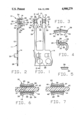
- FIG. 1 is a front view of a portion of a carrier strip and two solder terminals
- FIG. 2 is a sectional side view taken along line 2--2 of FIG. 1;
- FIGS. 3, 4 and 5 are sectional views taken, respectively, along lines 3--3 of FIG. 2; 4--4 of FIG. 3; and 5--5 of FIG. 1;
- FIG. 6 is a sectional view taken through the contact clip of a terminal as mounted on a substrate.
- FIG. 7 is a view similar to FIG. 6 shown after forming solder joints between the clip and pads on the substrate.
- Solder terminals 10 shown in FIG. 1 and 2 are formed from long, thin strips of metal 11 stamped from strip stock and joined to carrier strip 14.
- Each terminal includes a leg 12 attached to carrier strip 14 with a C-shaped contact clip 16 at the free end of the terminal.
- the clip includes a pair of opposed, like contact arms 18 joined together by bridge 20 to form an open substrate receiving-recess 22 between the interior surfaces of arms 18.
- Each arm has a base 23, formed of strip stock and a solder overlay.
- the base of the lower arm 18 away from bridge 20 is joined to the upper end of leg 12 by a diagonal strain relief connecting arm 24 extending down to the end of leg 12 and forming an opening 26 between arms 18 and 24.
- the bottom of opening 26 is defined by the reverse bend 27 at the junction between the arms 24 and 18. Openings 22 and 26 open on opposite sides of the terminal 10. See FIG. 1.
- the arm 24 is provided with a pair of standoff tabs 30 at the upper end of leg 12 used to support the terminal when leg 12 is inserted into a circuit board hole
- Carrier strip 14 is provided with a plurality of pilot holes 28 used to move the strip incrementally along a feed path.
- Alignment tabs 30 shown in FIG. 1 are bent out to one side of the strip and fit in a slot to hold the strip at a proper height in the path.
- the terminals 10 are stamp formed from flat strip stock having an integral solder overlay layer bonded to the portion of the stock forming the interior surfaces of the clip 16.
- the terminal 10 may be manufactured from strip stock having a thickness of about 0.010 inch and carrying an integral solder overlay 38 having a thickness of about 0.004 inch on the side forming the interior of the clip.
- each base 23 is bent down away from central contacts or ridges 36.
- the ridges face the opening 22, each extending away from the bridge toward the mouth of the opening.
- the ridges may be slightly convex. They oppose each other as shown in FIG. 2.
- solder layer 38 is thinned and extruded away from ridges 36 and beyond the edges of the clip arms as shown.
- the solder layer is reduced to a thickness of about 0.0005 inch, sufficient to provide light solder coatings covering the ridges.
- the solder 38 increases in thickness away from the ridge so that a considerable volume of solder is retained on the base, adjacent to the ridges and in contact with the solder on the ridges but at a level below the contact ridges.
- the solder on the ridges forms the high points of the arms.
- the solder is continuous with the solder on the inner surface of clip bridge 20.
- the arms 18 are bent down from ridges 36 to form corner recesses at the junction between each arm and the bridge and to provide smooth substrate lead ins at the mouth of recess 22.
- the contact clip 16 is manufactured with the opposed solder coated contact ridges 36 spaced apart a distance slightly less than the thickness of a substrate 42 inserted into the clip. When inserted, the substrate elastically deforms the bridge so that the insertion force is low yet the arms are resiliently held on the substrate pads 44. The contact pressure between the arms and the substrate is insufficient to scrape off the thin layers of solder overlying contact ridges 36. See FIG. 6 where the thickness of the solder at the ridges is exaggerated.
- the solder mass 38 on the inner convex surfaces of arms 18 surrounds ridges 36, has a minimum thickness at the ridges and increase in thickness away from the ridges but is below the ridges. Only the thin layers 37 engage pads 44.
- the contact ridges 36 are separated from the bridge 20 by corner recesses 40 thereby assuring that the lead end of the substrate does not engage the arms adjacent the base. Such engagement could bend open the clip, reduce the contact pressure between the clip and the substrate and allow the clip to fall off the substrate.
- the clip After the clip has been mounted on the substrate as shown in FIG. 6, the clip is heated to melt the solder layer 38 and form solder fillets 46 joining the arms 18 to pads 44 and extending 360 degrees around the contact ridges 36. Capillary action draws the molten solder from the entire inner surface of the clip, including the bridge, to the fillets 46. The solder coined beyond the edges of the clip is drawn into the fillet. The thin solder layer 37 at the ridges assures that solder is reliably drawn to the arm-substrate contact area to form a circumferentially continuous solder joint.
- soldering of terminals 10 to substrate 42 the terminals are severed from the carrier strip 14.
- the substrate and terminal assembly may then be mounted on a circuit board, typically by extending legs 12 through holes in the circuit board. Soldered connections may be formed between the legs and holes, conventionally by wave soldering. Alternatively, electrical connections may be formed with the substrate by mounting the substrate--terminal assembly in a connector block and forming connections between contacts in the block and legs 12.
Abstract
A solder terminal includes a clip adapted to be positioned on one edge of a substrate for forming soldered connections with substrate pads. A leg extends from the clip for forming an electrical connection with a circuit component.
Description
The invention relates to solder terminals, particularly solder clips for forming soldered connections with contact pads on the edges of substrates.
Conventional solder terminals include clips for mounting on the edges of substrates with the interior surfaces of the clips engaging contact pads on the substrate. The clips carry masses of solder remote from the clip-substrate contact such that when the mounted clips are heated the solder melts and must flow a distance to the contact to form a soldered joint. In production applications is difficult to assure that the solder reliably flows to the joint with the result that with this type of terminal there is a risk of forming an unreliable solder joint. Manufacture of these terminals requires forming a solder mass and securing the mass on the terminal. Specialized tooling and production techniques are required.
The present solder terminal is formed from a length of metal stamped from strip stock and includes a C-shaped clip for mounting on the edge of a substrate. The clip has a pair of opposed, like arms on opposite sides of the clip opening with each arm including a base having a central contact ridge facing into the opening and located above the rest of the base. A solder layer is provided on the inner surface of the arm and includes a thin coating overlying the ridge and a solder mass having an increased thickness away from the ridge. The solder overlying the ridge is the high point of the arm, with the solder away from the ridge being located below the thin coating.
The solder terminal is mounted on the substrate by moving the clip over the substrate edge so that the thin solder coating and ridge engage contact pads on the substrate. The substrate has a thickness slightly greater than the spacing between the two solder layers so that the flexible bridge at the back of the clip is stressed slightly to provide a light contact pressure between the arms and the pads, sufficient to hold the clip in place. Following mounting, the clip is heated to melt the solder layers. Capillary action draws the molten solder into the contact areas to form reliable solder fillets extending around the ridges and connecting the arms and the pads. The clip also includes a layer of solder on the bridge adjacent from the arms. Upon melting, this solder is also drawn into both contact areas and forms part of the fillets.
The solder terminals are preferably manufactured from strip stock having a solder inlay layer at the portion of the strip stock forming the clip. In this way, the terminal is manufactured in a simple stamping and forming operation without the necessity of providing a separate solder mass and a mechanism for securing the solder mass to the terminal.
Other objects and features of the invention will become apparent as the description proceeds, especially when taken in conjunction with the accompanying drawings illustrating the invention, of which there is one sheet and one embodiment.
FIG. 1 is a front view of a portion of a carrier strip and two solder terminals;
FIG. 2 is a sectional side view taken along line 2--2 of FIG. 1;
FIGS. 3, 4 and 5 are sectional views taken, respectively, along lines 3--3 of FIG. 2; 4--4 of FIG. 3; and 5--5 of FIG. 1;
FIG. 6 is a sectional view taken through the contact clip of a terminal as mounted on a substrate; and
FIG. 7 is a view similar to FIG. 6 shown after forming solder joints between the clip and pads on the substrate.
Solder terminals 10 shown in FIG. 1 and 2 are formed from long, thin strips of metal 11 stamped from strip stock and joined to carrier strip 14. Each terminal includes a leg 12 attached to carrier strip 14 with a C-shaped contact clip 16 at the free end of the terminal. The clip includes a pair of opposed, like contact arms 18 joined together by bridge 20 to form an open substrate receiving-recess 22 between the interior surfaces of arms 18. Each arm has a base 23, formed of strip stock and a solder overlay. The base of the lower arm 18 away from bridge 20 is joined to the upper end of leg 12 by a diagonal strain relief connecting arm 24 extending down to the end of leg 12 and forming an opening 26 between arms 18 and 24. The bottom of opening 26 is defined by the reverse bend 27 at the junction between the arms 24 and 18. Openings 22 and 26 open on opposite sides of the terminal 10. See FIG. 1. The arm 24 is provided with a pair of standoff tabs 30 at the upper end of leg 12 used to support the terminal when leg 12 is inserted into a circuit board hole or similar support.
Carrier strip 14 is provided with a plurality of pilot holes 28 used to move the strip incrementally along a feed path. Alignment tabs 30 shown in FIG. 1 are bent out to one side of the strip and fit in a slot to hold the strip at a proper height in the path.
The terminals 10 are stamp formed from flat strip stock having an integral solder overlay layer bonded to the portion of the stock forming the interior surfaces of the clip 16. For example, the terminal 10 may be manufactured from strip stock having a thickness of about 0.010 inch and carrying an integral solder overlay 38 having a thickness of about 0.004 inch on the side forming the interior of the clip.
During stamping and forming of the terminals from the strip stock the sides 34 and ends of each base 23 are bent down away from central contacts or ridges 36. When the clip is formed the ridges face the opening 22, each extending away from the bridge toward the mouth of the opening. The ridges may be slightly convex. They oppose each other as shown in FIG. 2.
As the clip 16 is formed the solder layer 38 is thinned and extruded away from ridges 36 and beyond the edges of the clip arms as shown. At the ridges 36 the solder layer is reduced to a thickness of about 0.0005 inch, sufficient to provide light solder coatings covering the ridges. As shown in FIGS. 3 and 4, the solder 38 increases in thickness away from the ridge so that a considerable volume of solder is retained on the base, adjacent to the ridges and in contact with the solder on the ridges but at a level below the contact ridges. The solder on the ridges forms the high points of the arms. The solder is continuous with the solder on the inner surface of clip bridge 20. This solder is also coined and extruded beyond the sides of the bridge 20. The arms 18 are bent down from ridges 36 to form corner recesses at the junction between each arm and the bridge and to provide smooth substrate lead ins at the mouth of recess 22.
The contact clip 16 is manufactured with the opposed solder coated contact ridges 36 spaced apart a distance slightly less than the thickness of a substrate 42 inserted into the clip. When inserted, the substrate elastically deforms the bridge so that the insertion force is low yet the arms are resiliently held on the substrate pads 44. The contact pressure between the arms and the substrate is insufficient to scrape off the thin layers of solder overlying contact ridges 36. See FIG. 6 where the thickness of the solder at the ridges is exaggerated. The solder mass 38 on the inner convex surfaces of arms 18 surrounds ridges 36, has a minimum thickness at the ridges and increase in thickness away from the ridges but is below the ridges. Only the thin layers 37 engage pads 44.
The contact ridges 36 are separated from the bridge 20 by corner recesses 40 thereby assuring that the lead end of the substrate does not engage the arms adjacent the base. Such engagement could bend open the clip, reduce the contact pressure between the clip and the substrate and allow the clip to fall off the substrate.
After the clip has been mounted on the substrate as shown in FIG. 6, the clip is heated to melt the solder layer 38 and form solder fillets 46 joining the arms 18 to pads 44 and extending 360 degrees around the contact ridges 36. Capillary action draws the molten solder from the entire inner surface of the clip, including the bridge, to the fillets 46. The solder coined beyond the edges of the clip is drawn into the fillet. The thin solder layer 37 at the ridges assures that solder is reliably drawn to the arm-substrate contact area to form a circumferentially continuous solder joint.
Following soldering of terminals 10 to substrate 42 the terminals are severed from the carrier strip 14. The substrate and terminal assembly may then be mounted on a circuit board, typically by extending legs 12 through holes in the circuit board. Soldered connections may be formed between the legs and holes, conventionally by wave soldering. Alternatively, electrical connections may be formed with the substrate by mounting the substrate--terminal assembly in a connector block and forming connections between contacts in the block and legs 12.
While I have illustrated and described a preferred embodiment of my invention, it is understood that this is capable of modification, and I therefore do not wish to be limited to the precise details set forth, but desire to avail myself of such changes and alterations as fall within the purview of the following claims.
Claims (20)
1. A solder terminal including a contact element and a contact arm joined to the element, the arm having a base with a central contact extending above the base and a solder layer overlying the base, the first solder layer including a thin coating overlying the contact forming the high point of the arm and having an increased thickness away from the contact to provide a mass of solder for forming a soldered joint at the contact when the arm is heated.
2. A solder terminal as in claim 1 wherein the thin coating is about 0.0005 inch thick.
3. A solder terminal as in claim 1 including a solder mass integral with said first solder layer and overlying a part of the terminal immediately adjacent to the base.
4. A solder terminal as in claim 1 wherein the contact comprises a ridge.
5. A solder terminal as in claim 1 wherein the solder layer extends beyond the edges of the base.
6. A solder terminal as in claim 1 including a second contact arm like said previously recited contact arm, a flexible bridge joining the arms with both arms extending in the same direction away from opposite ends of the bridge and with the contacts facing each other to form a C-shaped clip adapted to be mounted on a substrate.
7. A solder terminal as in claim 6 wherein the thin solder coatings are about 0.0005 inch thick.
8. A solder terminal as in claim 7 including a solder layer on the bridge integral with the solder layers on the bases.
9. A solder terminal as in claim 6 wherein said contacts comprises a ridge extending away from the bridge.
10. A solder terminal as in claim 9 wherein said contacts oppose each other.
11. A solder terminal as in claim 6 wherein the contact element comprises a straight leg integral with and extending away from the clip.
12. A solder terminal as in claim 11 including a strain relief arm extending from one end of the leg to an end of a contact arm away from the bridge, said leg and said bridge being generally coplanar.
13. A solder terminal as in claim 11 including alignment tabs extending laterally from opposite sides of the strain relief arm.
14. A solder terminal including a contact leg and a clip at one end of the leg, said clip including a pair of like opposed contact arms each including a base with a contact projection facing the other arm and a body of solder overlying the base, the body of solder including a thin layer extending over the projection and having an increasing thickness away from the projection, said projection forming the high point of the contact arm; and a resilient bridge joining the contact arm bases.
15. A solder terminal as in claim 14 wherein said clip includes a solder mass overlying the bridge and integral with the solder bodies on the contact arms.
16. A solder terminal as in claim 14 wherein said contact projections comprise opposed ridges extending away from the bridge.
17. A solder terminal as in claim 14 including an offset arm extending from one end of a contact arm away from the bridge back along such arm, said leg being joined to said offset arm and extending away from the clip.
18. A solder terminal as in claim 14 wherein the thin layer of each arm is about 0.0005 inch thick.
19. A solder terminal as in claim 18 including a solder mass on the bridge integral with the solder bodies on the arms.
20. A solder terminal as in claim 19 wherein the solder bodies extend beyond the edges of the clip.
Priority Applications (2)
| Application Number | Priority Date | Filing Date | Title |
|---|---|---|---|
| US07/342,102 US4900279A (en) | 1989-04-24 | 1989-04-24 | Solder terminal |
| EP19890311139 EP0394588A3 (en) | 1989-04-24 | 1989-10-27 | Solder terminal |
Applications Claiming Priority (1)
| Application Number | Priority Date | Filing Date | Title |
|---|---|---|---|
| US07/342,102 US4900279A (en) | 1989-04-24 | 1989-04-24 | Solder terminal |
Publications (1)
| Publication Number | Publication Date |
|---|---|
| US4900279A true US4900279A (en) | 1990-02-13 |
Family
ID=23340334
Family Applications (1)
| Application Number | Title | Priority Date | Filing Date |
|---|---|---|---|
| US07/342,102 Expired - Lifetime US4900279A (en) | 1989-04-24 | 1989-04-24 | Solder terminal |
Country Status (2)
| Country | Link |
|---|---|
| US (1) | US4900279A (en) |
| EP (1) | EP0394588A3 (en) |
Cited By (18)
| Publication number | Priority date | Publication date | Assignee | Title |
|---|---|---|---|---|
| US5015206A (en) * | 1990-04-05 | 1991-05-14 | Die Tech, Inc. | Solder terminal |
| WO1991016736A1 (en) * | 1990-04-13 | 1991-10-31 | North American Specialties Corporation | Solder-bearing lead |
| US5074806A (en) * | 1990-07-26 | 1991-12-24 | Amp Incorporated | Method and apparatus for coupling a connector to a cable |
| US5090926A (en) * | 1991-02-26 | 1992-02-25 | North American Specialties Corporation | Solderable lead |
| US5411420A (en) * | 1993-05-27 | 1995-05-02 | Die Tech, Inc. | Solder terminal strip |
| US5441429A (en) * | 1990-04-13 | 1995-08-15 | North American Specialties Corporation | Solder-bearing land |
| US5490788A (en) * | 1994-11-01 | 1996-02-13 | Emc Technology, Inc. | Surface mount terminal for electrical component |
| WO1996010279A1 (en) * | 1994-09-29 | 1996-04-04 | North American Specialties Corporation | Solder-bearing lead and method of producing and using same |
| US5569056A (en) * | 1993-05-14 | 1996-10-29 | Proner Comatel | Electrical connection device and process for the production thereof |
| US5601459A (en) * | 1994-09-29 | 1997-02-11 | North American Specialties Corporation | Solder bearing lead and method of fabrication |
| US5653617A (en) * | 1994-01-25 | 1997-08-05 | North American Specialties Corporation | Smart card connector |
| FR2761852A1 (en) * | 1997-04-08 | 1998-10-09 | Proner Comatel Sa | Perpendicular Board connection for Printed Circuit mother Boards |
| US6261136B1 (en) | 1999-04-30 | 2001-07-17 | Die Tech, Inc. | Edge clip terminal |
| US20050079763A1 (en) * | 1996-10-10 | 2005-04-14 | Lemke Timothy A. | High density connector and method of manufacture |
| EP1617519A2 (en) * | 1996-10-10 | 2006-01-18 | Fci | High density connector |
| US20080268676A1 (en) * | 2007-04-26 | 2008-10-30 | Teka Interconnections Systems, Inc. | Electrical connectors for use in soldering operations |
| US8851933B2 (en) | 2013-03-11 | 2014-10-07 | Kerdea Technologies, Inc. | Releasable electrical connection |
| WO2021006325A1 (en) * | 2019-07-10 | 2021-01-14 | 住友電工プリントサーキット株式会社 | Flexible printed wiring board, battery wiring module, and method for manufacturing flexible printed wiring board |
Families Citing this family (3)
| Publication number | Priority date | Publication date | Assignee | Title |
|---|---|---|---|---|
| JPH065137U (en) * | 1992-06-19 | 1994-01-21 | モレックス インコーポレーテッド | Terminals in surface mount electrical connectors |
| US5451174A (en) * | 1993-06-29 | 1995-09-19 | Autosplice Systems, Inc. | Surface mounted pins for printed circuit boards |
| FR2781610B1 (en) * | 1998-07-23 | 2000-10-13 | Proner Comatel Sa | ELECTRICAL CONTACT FOR MOUNTING A MODULE ON A RIGID CIRCUIT |
Citations (6)
| Publication number | Priority date | Publication date | Assignee | Title |
|---|---|---|---|---|
| US3324230A (en) * | 1965-08-23 | 1967-06-06 | Raychem Corp | Electrical connector with preplaced solder |
| US3750252A (en) * | 1972-05-01 | 1973-08-07 | Du Pont | Solder terminal strip |
| US4019803A (en) * | 1975-10-15 | 1977-04-26 | E. I. Du Pont De Nemours And Company | Solder substrate clip |
| US4203648A (en) * | 1977-08-15 | 1980-05-20 | North American Specialties Corp. | Solder bearing terminal |
| US4679889A (en) * | 1985-05-24 | 1987-07-14 | North American Specialties Corporation | Solder-bearing leads |
| US4718863A (en) * | 1986-05-02 | 1988-01-12 | Thomas & Betts Corporation | Jumper cable having clips for solder connections |
Family Cites Families (3)
| Publication number | Priority date | Publication date | Assignee | Title |
|---|---|---|---|---|
| US4427498A (en) * | 1982-03-25 | 1984-01-24 | Amp Incorporated | Selective plating interior surfaces of electrical terminals |
| US4486511A (en) * | 1983-06-27 | 1984-12-04 | National Semiconductor Corporation | Solder composition for thin coatings |
| US4673967A (en) * | 1985-01-29 | 1987-06-16 | Texas Instruments Incorporated | Surface mounted system for leaded semiconductor devices |
-
1989
- 1989-04-24 US US07/342,102 patent/US4900279A/en not_active Expired - Lifetime
- 1989-10-27 EP EP19890311139 patent/EP0394588A3/en not_active Withdrawn
Patent Citations (6)
| Publication number | Priority date | Publication date | Assignee | Title |
|---|---|---|---|---|
| US3324230A (en) * | 1965-08-23 | 1967-06-06 | Raychem Corp | Electrical connector with preplaced solder |
| US3750252A (en) * | 1972-05-01 | 1973-08-07 | Du Pont | Solder terminal strip |
| US4019803A (en) * | 1975-10-15 | 1977-04-26 | E. I. Du Pont De Nemours And Company | Solder substrate clip |
| US4203648A (en) * | 1977-08-15 | 1980-05-20 | North American Specialties Corp. | Solder bearing terminal |
| US4679889A (en) * | 1985-05-24 | 1987-07-14 | North American Specialties Corporation | Solder-bearing leads |
| US4718863A (en) * | 1986-05-02 | 1988-01-12 | Thomas & Betts Corporation | Jumper cable having clips for solder connections |
Cited By (27)
| Publication number | Priority date | Publication date | Assignee | Title |
|---|---|---|---|---|
| US5015206A (en) * | 1990-04-05 | 1991-05-14 | Die Tech, Inc. | Solder terminal |
| WO1991016736A1 (en) * | 1990-04-13 | 1991-10-31 | North American Specialties Corporation | Solder-bearing lead |
| US5344343A (en) * | 1990-04-13 | 1994-09-06 | North American Specialties Corporation | Solder-bearing lead |
| US5441429A (en) * | 1990-04-13 | 1995-08-15 | North American Specialties Corporation | Solder-bearing land |
| US5074806A (en) * | 1990-07-26 | 1991-12-24 | Amp Incorporated | Method and apparatus for coupling a connector to a cable |
| US5090926A (en) * | 1991-02-26 | 1992-02-25 | North American Specialties Corporation | Solderable lead |
| USRE35549E (en) * | 1991-02-26 | 1997-07-01 | North American Specialties Corporation | Solderable lead |
| US5569056A (en) * | 1993-05-14 | 1996-10-29 | Proner Comatel | Electrical connection device and process for the production thereof |
| US5411420A (en) * | 1993-05-27 | 1995-05-02 | Die Tech, Inc. | Solder terminal strip |
| US5653617A (en) * | 1994-01-25 | 1997-08-05 | North American Specialties Corporation | Smart card connector |
| WO1996010279A1 (en) * | 1994-09-29 | 1996-04-04 | North American Specialties Corporation | Solder-bearing lead and method of producing and using same |
| US5601459A (en) * | 1994-09-29 | 1997-02-11 | North American Specialties Corporation | Solder bearing lead and method of fabrication |
| US5490788A (en) * | 1994-11-01 | 1996-02-13 | Emc Technology, Inc. | Surface mount terminal for electrical component |
| US8167630B2 (en) | 1996-10-10 | 2012-05-01 | Fci Americas Technology Llc | High density connector and method of manufacture |
| US20050079763A1 (en) * | 1996-10-10 | 2005-04-14 | Lemke Timothy A. | High density connector and method of manufacture |
| EP1617519A2 (en) * | 1996-10-10 | 2006-01-18 | Fci | High density connector |
| US7186123B2 (en) | 1996-10-10 | 2007-03-06 | Fci Americas Technology, Inc. | High density connector and method of manufacture |
| EP1617519A3 (en) * | 1996-10-10 | 2007-12-12 | Fci | High density connector |
| US20080032524A1 (en) * | 1996-10-10 | 2008-02-07 | Lemke Timothy A | High Density Connector and Method of Manufacture |
| FR2761852A1 (en) * | 1997-04-08 | 1998-10-09 | Proner Comatel Sa | Perpendicular Board connection for Printed Circuit mother Boards |
| US6261136B1 (en) | 1999-04-30 | 2001-07-17 | Die Tech, Inc. | Edge clip terminal |
| US7758350B2 (en) * | 2007-04-26 | 2010-07-20 | Teka Interconnection Systems | Electrical connector with solder retention means for assembly |
| CN101682126B (en) * | 2007-04-26 | 2011-11-30 | 东恺互联系统公司 | Electrical connector for electrically connecting the first electronic device to the second electronic device and method therefor |
| US20080268676A1 (en) * | 2007-04-26 | 2008-10-30 | Teka Interconnections Systems, Inc. | Electrical connectors for use in soldering operations |
| US8851933B2 (en) | 2013-03-11 | 2014-10-07 | Kerdea Technologies, Inc. | Releasable electrical connection |
| WO2021006325A1 (en) * | 2019-07-10 | 2021-01-14 | 住友電工プリントサーキット株式会社 | Flexible printed wiring board, battery wiring module, and method for manufacturing flexible printed wiring board |
| US20220272839A1 (en) * | 2019-07-10 | 2022-08-25 | Sumitomo Electric Printed Circuits, Inc. | Flexible printed wiring board, battery wiring module, and method of manufacturing flexible printed wiring board |
Also Published As
| Publication number | Publication date |
|---|---|
| EP0394588A3 (en) | 1990-12-27 |
| EP0394588A2 (en) | 1990-10-31 |
Similar Documents
| Publication | Publication Date | Title |
|---|---|---|
| US4900279A (en) | Solder terminal | |
| US4679889A (en) | Solder-bearing leads | |
| EP0215024B1 (en) | Solder-bearing terminal | |
| US6997727B1 (en) | Compliant surface mount electrical contacts for circuit boards and method of making and using same | |
| US4302067A (en) | Edge connectors for circuit cards and methods of assembly | |
| US4597628A (en) | Solder bearing clip | |
| US5015206A (en) | Solder terminal | |
| US4797110A (en) | Printed circuit board with integral electrical connector and method for making it using wave soldering | |
| US4728305A (en) | Solder-bearing leads | |
| KR19980024740A (en) | Interference fit pin for printed circuit board | |
| US5823801A (en) | Electrical connector having thin contacts with surface mount edges | |
| US5052954A (en) | Solder-bearing terminal pin and lead | |
| CN216698775U (en) | Electrical contact for connecting substrates together and electrical assembly including same | |
| US3953102A (en) | Terminal clip for micromodule | |
| JP3085572B2 (en) | Connection terminal | |
| US4556276A (en) | Solder beams leads | |
| US6508664B2 (en) | Connectors for circuit boards configured with foil on both sides | |
| US5090926A (en) | Solderable lead | |
| EP1147573B1 (en) | Collapsible electrical leads for engaging a substrate | |
| EP0546679A1 (en) | Contact | |
| US4357510A (en) | Switch device for use on circuit board | |
| JP2000277194A (en) | Fitting type connecting terminal | |
| AU583396B2 (en) | Solder bearing leads | |
| JPH0615416Y2 (en) | Chip type socket | |
| EP0116073B1 (en) | Solder bearing edge clip |
Legal Events
| Date | Code | Title | Description |
|---|---|---|---|
| AS | Assignment |
Owner name: DIE TECH, INC., PENNSYLVANIA Free format text: ASSIGNMENT OF ASSIGNORS INTEREST.;ASSIGNOR:DENNIS, RICHARD K.;REEL/FRAME:005175/0223 Effective date: 19890410 |
|
| STCF | Information on status: patent grant |
Free format text: PATENTED CASE |
|
| FPAY | Fee payment |
Year of fee payment: 4 |
|
| CC | Certificate of correction | ||
| FPAY | Fee payment |
Year of fee payment: 8 |
|
| FEPP | Fee payment procedure |
Free format text: PAYOR NUMBER ASSIGNED (ORIGINAL EVENT CODE: ASPN); ENTITY STATUS OF PATENT OWNER: SMALL ENTITY |
|
| FPAY | Fee payment |
Year of fee payment: 12 |