US4900689A - Method of fabrication of isolated islands for complementary bipolar devices - Google Patents
Method of fabrication of isolated islands for complementary bipolar devices Download PDFInfo
- Publication number
- US4900689A US4900689A US07/281,546 US28154688A US4900689A US 4900689 A US4900689 A US 4900689A US 28154688 A US28154688 A US 28154688A US 4900689 A US4900689 A US 4900689A
- Authority
- US
- United States
- Prior art keywords
- region
- forming
- mask
- layer
- process according
- Prior art date
- Legal status (The legal status is an assumption and is not a legal conclusion. Google has not performed a legal analysis and makes no representation as to the accuracy of the status listed.)
- Expired - Lifetime
Links
- 230000000295 complement effect Effects 0.000 title claims abstract description 12
- 238000004519 manufacturing process Methods 0.000 title description 6
- 238000000034 method Methods 0.000 claims abstract description 34
- 238000002955 isolation Methods 0.000 claims abstract description 23
- 239000000758 substrate Substances 0.000 claims abstract description 20
- 230000002401 inhibitory effect Effects 0.000 claims description 29
- 239000012535 impurity Substances 0.000 claims description 20
- 238000001020 plasma etching Methods 0.000 claims description 6
- 238000005530 etching Methods 0.000 claims description 5
- 230000001590 oxidative effect Effects 0.000 claims description 5
- 238000004518 low pressure chemical vapour deposition Methods 0.000 claims description 2
- 239000000463 material Substances 0.000 claims description 2
- 239000004065 semiconductor Substances 0.000 claims 6
- 238000009413 insulation Methods 0.000 claims 1
- 239000012212 insulator Substances 0.000 claims 1
- 150000004767 nitrides Chemical class 0.000 claims 1
- 230000008021 deposition Effects 0.000 abstract description 5
- VYPSYNLAJGMNEJ-UHFFFAOYSA-N Silicium dioxide Chemical compound O=[Si]=O VYPSYNLAJGMNEJ-UHFFFAOYSA-N 0.000 description 10
- XUIMIQQOPSSXEZ-UHFFFAOYSA-N Silicon Chemical compound [Si] XUIMIQQOPSSXEZ-UHFFFAOYSA-N 0.000 description 9
- 229910052710 silicon Inorganic materials 0.000 description 9
- 239000010703 silicon Substances 0.000 description 9
- 230000000873 masking effect Effects 0.000 description 8
- 235000012239 silicon dioxide Nutrition 0.000 description 5
- 239000000377 silicon dioxide Substances 0.000 description 5
- 238000000151 deposition Methods 0.000 description 4
- 238000005516 engineering process Methods 0.000 description 4
- 230000003647 oxidation Effects 0.000 description 4
- 238000007254 oxidation reaction Methods 0.000 description 4
- 229920002120 photoresistant polymer Polymers 0.000 description 4
- 230000015572 biosynthetic process Effects 0.000 description 3
- 238000005229 chemical vapour deposition Methods 0.000 description 3
- 229910052581 Si3N4 Inorganic materials 0.000 description 2
- 238000009792 diffusion process Methods 0.000 description 2
- HQVNEWCFYHHQES-UHFFFAOYSA-N silicon nitride Chemical compound N12[Si]34N5[Si]62N3[Si]51N64 HQVNEWCFYHHQES-UHFFFAOYSA-N 0.000 description 2
- 238000007704 wet chemistry method Methods 0.000 description 2
- BLRPTPMANUNPDV-UHFFFAOYSA-N Silane Chemical compound [SiH4] BLRPTPMANUNPDV-UHFFFAOYSA-N 0.000 description 1
- PBZHKWVYRQRZQC-UHFFFAOYSA-N [Si+4].[O-][N+]([O-])=O.[O-][N+]([O-])=O.[O-][N+]([O-])=O.[O-][N+]([O-])=O Chemical compound [Si+4].[O-][N+]([O-])=O.[O-][N+]([O-])=O.[O-][N+]([O-])=O.[O-][N+]([O-])=O PBZHKWVYRQRZQC-UHFFFAOYSA-N 0.000 description 1
- 239000013078 crystal Substances 0.000 description 1
- 230000007423 decrease Effects 0.000 description 1
- 230000000694 effects Effects 0.000 description 1
- 238000005468 ion implantation Methods 0.000 description 1
- 239000000203 mixture Substances 0.000 description 1
- 229910021420 polycrystalline silicon Inorganic materials 0.000 description 1
- 229910000077 silane Inorganic materials 0.000 description 1
- 239000007858 starting material Substances 0.000 description 1
Images
Classifications
-
- H—ELECTRICITY
- H01—ELECTRIC ELEMENTS
- H01L—SEMICONDUCTOR DEVICES NOT COVERED BY CLASS H10
- H01L29/00—Semiconductor devices adapted for rectifying, amplifying, oscillating or switching, or capacitors or resistors with at least one potential-jump barrier or surface barrier, e.g. PN junction depletion layer or carrier concentration layer; Details of semiconductor bodies or of electrodes thereof ; Multistep manufacturing processes therefor
- H01L29/66—Types of semiconductor device ; Multistep manufacturing processes therefor
- H01L29/68—Types of semiconductor device ; Multistep manufacturing processes therefor controllable by only the electric current supplied, or only the electric potential applied, to an electrode which does not carry the current to be rectified, amplified or switched
- H01L29/70—Bipolar devices
- H01L29/72—Transistor-type devices, i.e. able to continuously respond to applied control signals
- H01L29/73—Bipolar junction transistors
- H01L29/7317—Bipolar thin film transistors
-
- H—ELECTRICITY
- H01—ELECTRIC ELEMENTS
- H01L—SEMICONDUCTOR DEVICES NOT COVERED BY CLASS H10
- H01L21/00—Processes or apparatus adapted for the manufacture or treatment of semiconductor or solid state devices or of parts thereof
- H01L21/70—Manufacture or treatment of devices consisting of a plurality of solid state components formed in or on a common substrate or of parts thereof; Manufacture of integrated circuit devices or of parts thereof
- H01L21/71—Manufacture of specific parts of devices defined in group H01L21/70
- H01L21/76—Making of isolation regions between components
- H01L21/762—Dielectric regions, e.g. EPIC dielectric isolation, LOCOS; Trench refilling techniques, SOI technology, use of channel stoppers
- H01L21/7624—Dielectric regions, e.g. EPIC dielectric isolation, LOCOS; Trench refilling techniques, SOI technology, use of channel stoppers using semiconductor on insulator [SOI] technology
- H01L21/76264—SOI together with lateral isolation, e.g. using local oxidation of silicon, or dielectric or polycristalline material refilled trench or air gap isolation regions, e.g. completely isolated semiconductor islands
-
- H—ELECTRICITY
- H01—ELECTRIC ELEMENTS
- H01L—SEMICONDUCTOR DEVICES NOT COVERED BY CLASS H10
- H01L21/00—Processes or apparatus adapted for the manufacture or treatment of semiconductor or solid state devices or of parts thereof
- H01L21/70—Manufacture or treatment of devices consisting of a plurality of solid state components formed in or on a common substrate or of parts thereof; Manufacture of integrated circuit devices or of parts thereof
- H01L21/77—Manufacture or treatment of devices consisting of a plurality of solid state components or integrated circuits formed in, or on, a common substrate
- H01L21/78—Manufacture or treatment of devices consisting of a plurality of solid state components or integrated circuits formed in, or on, a common substrate with subsequent division of the substrate into plural individual devices
- H01L21/82—Manufacture or treatment of devices consisting of a plurality of solid state components or integrated circuits formed in, or on, a common substrate with subsequent division of the substrate into plural individual devices to produce devices, e.g. integrated circuits, each consisting of a plurality of components
- H01L21/822—Manufacture or treatment of devices consisting of a plurality of solid state components or integrated circuits formed in, or on, a common substrate with subsequent division of the substrate into plural individual devices to produce devices, e.g. integrated circuits, each consisting of a plurality of components the substrate being a semiconductor, using silicon technology
- H01L21/8222—Bipolar technology
- H01L21/8228—Complementary devices, e.g. complementary transistors
- H01L21/82285—Complementary vertical transistors
-
- H—ELECTRICITY
- H01—ELECTRIC ELEMENTS
- H01L—SEMICONDUCTOR DEVICES NOT COVERED BY CLASS H10
- H01L21/00—Processes or apparatus adapted for the manufacture or treatment of semiconductor or solid state devices or of parts thereof
- H01L21/70—Manufacture or treatment of devices consisting of a plurality of solid state components formed in or on a common substrate or of parts thereof; Manufacture of integrated circuit devices or of parts thereof
- H01L21/71—Manufacture of specific parts of devices defined in group H01L21/70
- H01L21/76—Making of isolation regions between components
- H01L21/762—Dielectric regions, e.g. EPIC dielectric isolation, LOCOS; Trench refilling techniques, SOI technology, use of channel stoppers
- H01L21/7624—Dielectric regions, e.g. EPIC dielectric isolation, LOCOS; Trench refilling techniques, SOI technology, use of channel stoppers using semiconductor on insulator [SOI] technology
- H01L21/76264—SOI together with lateral isolation, e.g. using local oxidation of silicon, or dielectric or polycristalline material refilled trench or air gap isolation regions, e.g. completely isolated semiconductor islands
- H01L21/76275—Vertical isolation by bonding techniques
-
- H—ELECTRICITY
- H01—ELECTRIC ELEMENTS
- H01L—SEMICONDUCTOR DEVICES NOT COVERED BY CLASS H10
- H01L21/00—Processes or apparatus adapted for the manufacture or treatment of semiconductor or solid state devices or of parts thereof
- H01L21/70—Manufacture or treatment of devices consisting of a plurality of solid state components formed in or on a common substrate or of parts thereof; Manufacture of integrated circuit devices or of parts thereof
- H01L21/71—Manufacture of specific parts of devices defined in group H01L21/70
- H01L21/76—Making of isolation regions between components
- H01L21/762—Dielectric regions, e.g. EPIC dielectric isolation, LOCOS; Trench refilling techniques, SOI technology, use of channel stoppers
- H01L21/7624—Dielectric regions, e.g. EPIC dielectric isolation, LOCOS; Trench refilling techniques, SOI technology, use of channel stoppers using semiconductor on insulator [SOI] technology
- H01L21/76264—SOI together with lateral isolation, e.g. using local oxidation of silicon, or dielectric or polycristalline material refilled trench or air gap isolation regions, e.g. completely isolated semiconductor islands
- H01L21/76286—Lateral isolation by refilling of trenches with polycristalline material
Definitions
- the present invention relates generally to a method of fabricating isolated islands and more specifically to a method of fabricating isolated islands for complementary bipolar transistors.
- Another object of the present invention is to provide a method of fabricating isolated complementary bipolar transistors capable of high frequency operation.
- a still further object of the present invention is to provide a dielectrically isolated complementary bipolar transistor having reduced resistance buried collector portions.
- An even further object is to produce isolated complementary bipolar transistors with fewer process steps, including fewer photoresist masking steps and increased mask precision.
- first and second buried regions of opposite conductivity type in first and second regions of a horizontally isolated substrate.
- the horizontal isolation may be a dielectric or junction isolation.
- a first mask is formed over the second region and exposing the first region, and a third region of the first conductivity type is epitaxially deposited over the first region to the thickness of the mask and having a lower impurity concentration region than the buried first region.
- the first mask is removed and a second mask is formed by self-aligning technique over the third region and exposing the second region.
- a fourth region of the second conductivity region and a lower impurity concentration region than the second buried region is formed by epitaxial deposition having a thickness equal to the third region.
- a dielectric isolation region is then formed at adjacent lateral portions of the third and fourth region and the first and second buried regions.
- the third and fourth regions form collector regions and impurities are introduced to form appropriate base and emitter regions for the complementary bipolar transistors.
- the number of steps of masking is substantially reduced and the precision mask alignment is increased by using a self-alignment technique.
- the first mask is formed of a first oxide inhibiting layer followed by a first mask layer.
- the second mask is formed by removing the first mask layer, oxidizing using the first mask inhibiting layer as a mask to form a second mask layer of oxide over the third region and exposing the second region.
- the first oxide inhibiting mask layer is then removed.
- forming the second mask includes applying a second oxide inhibiting mask layer before oxidizing to cover the exposed portion of the top and side edges of the third region. Using, for example, reactive ion etching, the second oxide inhibiting layer is removed to form horizontal surfaces which include the top of the third region leaving the second oxide inhibiting layer on the lateral edges of the third region.
- the formation of the dielectric isolated region includes removing adjacent portions of the third and fourth region and first and second buried region to form a trench.
- the exposed surfaces are then covered with an insulative layer and the trench is filled with a polycrystalline material.
- the trench is formed down to the horizontal isolation.
- the horizontal isolation may be a horizontal dielectric layer or may be a PN junction.
- FIGS. 1-12 are cross-sectional views of a wafer at various stages of fabrication according to the principles of the present invention for a completely dielectrically isolated island.
- FIG. 13 is a cross-sectional view of the resulting product of the present invention applied to horizontal junction isolated regions with lateral dielectrical isolation.
- FIG. 14 is a cross-sectional view of complementary bipolar transistors in dielectrically isolated regions according to the principles of the present application.
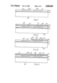
- a starting material or wafer handle 20 may be an oxidized silicon wafer having a thin single crystalline layer or substrate, for example silicon, 24 secured thereto by, for example, oxide bonding including a silicon dioxide layer 22 or other suitable technologies.
- the silicon layer 24 may have a thickness in the range of 1 to 5 microns, although the thickness tolerance is not critical since it does not form the defining portion of the bipolar transistors.
- the doping level also is not important, and may be assumed to be lightly doped N-type silicon.
- a silicon dioxide layer 22 forms the bottom or horizontal portion of the isolation system. Using appropriate masks, N+ impurities and P+ impurities are introduced to form N+ buried region 26 and P+ buried region 28. These may be formed by conventional masking techniques and include either deposition and diffusion or ion implantation. The resulting structure, as illustrated in FIG. 1, will form the low resistivity buried collector contact regions.
- a masking layer 32 is then formed and may be, for example, an oxide formed by chemical vapor deposition of silox.
- the thickness of the masking layer 32 will define the thickness of the to be formed epitaxial layers which form the active regions of the bipolar transistors, namely generally the collectors. For ultra-high frequency transistors, the thickness of the masking layer 32 is in the range of 1.5 microns and may be anywhere from 1 to 4 microns.
- the resulting structure is illustrated in FIG. 2.
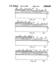
- first mask selected portions of the mask layer 32 and the first oxide inhibited layer 30 must be removed. This can be done by standard photoresist and etching techniques. Since it is important that the mask have a vertical wall on the remaining mask layer 32 and oxide inhibiting layer 30, preferably reactive ion etching is used.
- FIG. 3 The resulting structure is shown in FIG. 3 wherein an opening 34 is formed exposing the N+ buried layer 26 and a first region of the substrate 24.
- Epitaxial deposition is then performed which selectively forms a silicon layer 36 on the exposed portion of the substrate 24.
- the first epitaxial layer 36 is formed to the height of the first mask including oxide inhibiting layer 30 and the mask layer 32.
- no grain formation occurs on the surface of the silicon dioxide layer 32 and good quality epitaxial film is deposited on the exposed silicon surface of substrate 24.
- the conditions which allow this to happen are low pressure and low temperature epitaxial deposition using, for example, trichlore or silane, as a gas source.
- a typical example of the pressure range and temperature range are 40 to 80 millitorr for the pressure and 750 to 950 degrees centigrade for the temperature.
- the resulting epitaxial layer 36 is doped with, for example, N- impurity concentration.
- the resulting structure is shown in FIG. 4.
- the process then proceeds with the formation of the second mask.
- the first masking layer 32 is removed by, for example, wet chemistry.
- a second oxide inhibiting layer 38 is then formed. As previously, this is preceded by a thin oxide growth which is not illustrated.
- the second oxide inhibiting layer 38 is formed over the exposed portions of the N epitaxial layer 36, its horizontal and side edges, as well as on the first oxide layer 30.
- the second oxide inhibiting layer 38 is thinner than the first oxide inhibiting layer 30 and is generally about half the thickness.
- the resulting structure is illustrated in FIG. 5.
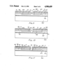
- the second oxide inhibiting layer which may also be silicon nitrate, is selectively removed from the horizontal surfaces by reactive ion etching. This removes the layer 38 from the top of the epitaxial layer 36 as well as over the first oxide inhibitive layer 30. It leaves the layer 38 on the lateral edges of the epitaxial layer 36.
- the wafer is then exposed to an oxidizing atmosphere to form an oxide layer 40 as a second mask only over the epitaxial region 36. The resulting structure is illustrated in FIG. 6.
- the oxide inhibiting layer 30 and 38 are selectively removed. This will produce a step where the epitaxial layer 36 is covered with the silicon dioxide mask 40 while the silicon surface is bare above the P+ buried layer 28. This is illustrated specifically in FIG. 7. It should be noted that there was no need for a second photoresist step. Thus, the double oxide inhibiting layer results in a self-aligned technology.
- a second selective epitaxial silicon film is grown on the exposed silicon region resulting in P-type impurity region over the buried region 28.
- the resulting structure is illustrated in FIG. 8.
- the epitaxial layer 42 is formed to the height of the first epitaxial layer 36.
- this poor quality film is not expected to extend laterally further than the thickness of the epitaxial layer itself.
- this region is approximately 1.5 microns.
- the first epitaxial layer 36 may be grown non-selectively our the over the total substrate 24.
- a layer of oxide equivalent to layer 40 of FIG. 6 may then be formed on the oxide layer and the oxide layer and first epitaxial layer 36 are selectively removed by etching to produce the structure illustrated in FIG. 7.
- the second epitaxial layer is then grown selectively and self-aligned as in the previous process.
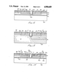
- the lateral isolation is formed as follows.
- the masking layer 40 is removed by a well-known technique from the surface of the N epitaxial layer 26.
- a new mask layer 44 is formed by, for example, oxidation. This may include chemical vapor deposition, as well as thermal oxidation.
- the mask layer 44 is then patterned by, for example, photoresist technique and etching, to provide an opening 46 exposing the adjacent regions of epitaxial layers 26 and 32.
- the resulting structure is illustrated in FIG. 9.
- a deep trench 48 is etched through the epitaxial layers 26 and 32 and the base region 24 down to the horizontal dielectric layer 22, as illustrated in FIG. 10. This may be performed by reactive ion etching. The amount removed will generally encompass the 1.5 micron region having the poor grain boundary.
- trench 48 The walls of trench 48 are then oxidized to form a silicon dioxide layer 50 on the walls of the trench. This may be performed by thermal oxidation or a combination of thermal oxidation and chemical vapor deposition.
- the resulting structure is illustrated in FIG. 11.
- the trenches then can be refilled with polycrystalline silicon and planarized using well-known techniques.
- the resulting structure containing N+ and P+ buried regions that are covered by N-type and P-type epitaxial layers respectively are dielectrically isolated and planarized as illustrated in FIG. 12.
- the process as described may also be used with a junction isolation along the bottom of the regions.
- the original substrate 54 may be a P-type substrate having an N pocket 56 formed therein.
- the N+ buried region 26 is then formed in the substrate 54 and the P+ buried region is formed in the N pocket 56.
- the process is then the same as described in FIGS. 2-9.
- the etching is performed down to the horizontal isolation which in this case is the PN junction between the substrate 54 and the N pocket 56.
- FIG. 11 and 12 are then continued to produce the lateral dielectric isolation in combination with horizontal junction isolation.
- bipolar transistors are then formed in the epitaxial region 36 and 42.
- P-type impurities are introduced to form a base region 60 in N collector region 36.
- N-type impurities are introduced into base regions 60 to form an N-type emitter region 62. This produces an NPN transistor.
- N-type impurities are introduced to form a base region 64 in the P epitaxial collector region 42.
- P-type impurities are introduced to form a P-type emitter region 66 in the base region 64. This produces a PNP transistor in the epitaxial layer 42.
Abstract
Description
Claims (17)
Priority Applications (1)
| Application Number | Priority Date | Filing Date | Title |
|---|---|---|---|
| US07/281,546 US4900689A (en) | 1988-12-08 | 1988-12-08 | Method of fabrication of isolated islands for complementary bipolar devices |
Applications Claiming Priority (1)
| Application Number | Priority Date | Filing Date | Title |
|---|---|---|---|
| US07/281,546 US4900689A (en) | 1988-12-08 | 1988-12-08 | Method of fabrication of isolated islands for complementary bipolar devices |
Publications (1)
| Publication Number | Publication Date |
|---|---|
| US4900689A true US4900689A (en) | 1990-02-13 |
Family
ID=23077744
Family Applications (1)
| Application Number | Title | Priority Date | Filing Date |
|---|---|---|---|
| US07/281,546 Expired - Lifetime US4900689A (en) | 1988-12-08 | 1988-12-08 | Method of fabrication of isolated islands for complementary bipolar devices |
Country Status (1)
| Country | Link |
|---|---|
| US (1) | US4900689A (en) |
Cited By (17)
| Publication number | Priority date | Publication date | Assignee | Title |
|---|---|---|---|---|
| US5039625A (en) * | 1990-04-27 | 1991-08-13 | Mcnc | Maximum areal density recessed oxide isolation (MADROX) process |
| US5225358A (en) * | 1991-06-06 | 1993-07-06 | Lsi Logic Corporation | Method of forming late isolation with polishing |
| US5248625A (en) * | 1991-06-06 | 1993-09-28 | Lsi Logic Corporation | Techniques for forming isolation structures |
| US5252503A (en) * | 1991-06-06 | 1993-10-12 | Lsi Logic Corporation | Techniques for forming isolation structures |
| US5286996A (en) * | 1991-12-31 | 1994-02-15 | Purdue Research Foundation | Triple self-aligned bipolar junction transistor |
| US5298110A (en) * | 1991-06-06 | 1994-03-29 | Lsi Logic Corporation | Trench planarization techniques |
| US5298786A (en) * | 1990-12-06 | 1994-03-29 | International Business Machines Corp. | SOI lateral bipolar transistor with edge-strapped base contact and method of fabricating same |
| US5344785A (en) * | 1992-03-13 | 1994-09-06 | United Technologies Corporation | Method of forming high speed, high voltage fully isolated bipolar transistors on a SOI substrate |
| US5413966A (en) * | 1990-12-20 | 1995-05-09 | Lsi Logic Corporation | Shallow trench etch |
| US5512774A (en) * | 1988-02-08 | 1996-04-30 | Kabushiki Kaisha Toshiba | Dielectrically isolated substrate and semiconductor device using the same |
| US5668397A (en) * | 1991-09-27 | 1997-09-16 | Harris Corp. | High frequency analog transistors, method of fabrication and circuit implementation |
| US5688702A (en) * | 1988-02-08 | 1997-11-18 | Kabushiki Kaisha Toshiba | Process of making a semiconductor device using a silicon-on-insulator substrate |
| US5721147A (en) * | 1995-09-29 | 1998-02-24 | Samsung Electronics Co., Ltd. | Methods of forming bipolar junction transistors |
| US5811868A (en) * | 1996-12-20 | 1998-09-22 | International Business Machines Corp. | Integrated high-performance decoupling capacitor |
| US5814538A (en) * | 1996-03-19 | 1998-09-29 | Samsung Electronics Co., Ltd. | Methods of forming BiCMOS devices having dual-layer emitter electrodes and thin-film transistors therein |
| US5994196A (en) * | 1997-04-01 | 1999-11-30 | Samsung Electronics Co., Ltd. | Methods of forming bipolar junction transistors using simultaneous base and emitter diffusion techniques |
| US6087244A (en) * | 1996-10-17 | 2000-07-11 | Fairchild Korea Semiconductor, Ltd. | Methods of forming semiconductor-on-insulator devices including buried layers of opposite conductivity type |
Citations (4)
| Publication number | Priority date | Publication date | Assignee | Title |
|---|---|---|---|---|
| US3793088A (en) * | 1972-11-15 | 1974-02-19 | Bell Telephone Labor Inc | Compatible pnp and npn devices in an integrated circuit |
| JPS5742144A (en) * | 1980-08-28 | 1982-03-09 | Fujitsu Ltd | Manufacture of semiconductor device |
| JPS58168258A (en) * | 1982-03-30 | 1983-10-04 | Nippon Telegr & Teleph Corp <Ntt> | Semiconductor integrated circuit device and manufacture thereof |
| US4719185A (en) * | 1986-04-28 | 1988-01-12 | International Business Machines Corporation | Method of making shallow junction complementary vertical bipolar transistor pair |
-
1988
- 1988-12-08 US US07/281,546 patent/US4900689A/en not_active Expired - Lifetime
Patent Citations (4)
| Publication number | Priority date | Publication date | Assignee | Title |
|---|---|---|---|---|
| US3793088A (en) * | 1972-11-15 | 1974-02-19 | Bell Telephone Labor Inc | Compatible pnp and npn devices in an integrated circuit |
| JPS5742144A (en) * | 1980-08-28 | 1982-03-09 | Fujitsu Ltd | Manufacture of semiconductor device |
| JPS58168258A (en) * | 1982-03-30 | 1983-10-04 | Nippon Telegr & Teleph Corp <Ntt> | Semiconductor integrated circuit device and manufacture thereof |
| US4719185A (en) * | 1986-04-28 | 1988-01-12 | International Business Machines Corporation | Method of making shallow junction complementary vertical bipolar transistor pair |
Cited By (21)
| Publication number | Priority date | Publication date | Assignee | Title |
|---|---|---|---|---|
| US5688702A (en) * | 1988-02-08 | 1997-11-18 | Kabushiki Kaisha Toshiba | Process of making a semiconductor device using a silicon-on-insulator substrate |
| US5512774A (en) * | 1988-02-08 | 1996-04-30 | Kabushiki Kaisha Toshiba | Dielectrically isolated substrate and semiconductor device using the same |
| US5039625A (en) * | 1990-04-27 | 1991-08-13 | Mcnc | Maximum areal density recessed oxide isolation (MADROX) process |
| US5298786A (en) * | 1990-12-06 | 1994-03-29 | International Business Machines Corp. | SOI lateral bipolar transistor with edge-strapped base contact and method of fabricating same |
| US5413966A (en) * | 1990-12-20 | 1995-05-09 | Lsi Logic Corporation | Shallow trench etch |
| US5441094A (en) * | 1991-06-06 | 1995-08-15 | Lsi Logic Corporation | Trench planarization techniques |
| US5225358A (en) * | 1991-06-06 | 1993-07-06 | Lsi Logic Corporation | Method of forming late isolation with polishing |
| US5312770A (en) * | 1991-06-06 | 1994-05-17 | Lsi Logic Corporation | Techniques for forming isolation structures |
| US5298110A (en) * | 1991-06-06 | 1994-03-29 | Lsi Logic Corporation | Trench planarization techniques |
| US5252503A (en) * | 1991-06-06 | 1993-10-12 | Lsi Logic Corporation | Techniques for forming isolation structures |
| US5248625A (en) * | 1991-06-06 | 1993-09-28 | Lsi Logic Corporation | Techniques for forming isolation structures |
| US5668397A (en) * | 1991-09-27 | 1997-09-16 | Harris Corp. | High frequency analog transistors, method of fabrication and circuit implementation |
| US5382828A (en) * | 1991-12-31 | 1995-01-17 | Purdue Research Foundation | Triple self-aligned bipolar junction transistor |
| US5434092A (en) * | 1991-12-31 | 1995-07-18 | Purdue Research Foundation | Method for fabricating a triple self-aligned bipolar junction transistor |
| US5286996A (en) * | 1991-12-31 | 1994-02-15 | Purdue Research Foundation | Triple self-aligned bipolar junction transistor |
| US5344785A (en) * | 1992-03-13 | 1994-09-06 | United Technologies Corporation | Method of forming high speed, high voltage fully isolated bipolar transistors on a SOI substrate |
| US5721147A (en) * | 1995-09-29 | 1998-02-24 | Samsung Electronics Co., Ltd. | Methods of forming bipolar junction transistors |
| US5814538A (en) * | 1996-03-19 | 1998-09-29 | Samsung Electronics Co., Ltd. | Methods of forming BiCMOS devices having dual-layer emitter electrodes and thin-film transistors therein |
| US6087244A (en) * | 1996-10-17 | 2000-07-11 | Fairchild Korea Semiconductor, Ltd. | Methods of forming semiconductor-on-insulator devices including buried layers of opposite conductivity type |
| US5811868A (en) * | 1996-12-20 | 1998-09-22 | International Business Machines Corp. | Integrated high-performance decoupling capacitor |
| US5994196A (en) * | 1997-04-01 | 1999-11-30 | Samsung Electronics Co., Ltd. | Methods of forming bipolar junction transistors using simultaneous base and emitter diffusion techniques |
Similar Documents
| Publication | Publication Date | Title |
|---|---|---|
| CA1159966A (en) | Process of forming recessed dielectric regions in a monocrystalline silicon substrate | |
| US4139442A (en) | Reactive ion etching method for producing deep dielectric isolation in silicon | |
| US4771328A (en) | Semiconductor device and process | |
| EP0036111B1 (en) | Method for making fine deep dielectric isolation | |
| EP0020994B1 (en) | Method for making isolation trenches | |
| EP0098374B1 (en) | Isolated dielectric structure for integrated circuits and method for fabricating such structure | |
| US4757028A (en) | Process for preparing a silicon carbide device | |
| US4900689A (en) | Method of fabrication of isolated islands for complementary bipolar devices | |
| US4638347A (en) | Gate electrode sidewall isolation spacer for field effect transistors | |
| EP0724291B1 (en) | Semiconductor device having an improved trench isolation and method for forming the same | |
| US4056413A (en) | Etching method for flattening a silicon substrate utilizing an anisotropic alkali etchant | |
| US5920108A (en) | Late process method and apparatus for trench isolation | |
| US3943542A (en) | High reliability, low leakage, self-aligned silicon gate FET and method of fabricating same | |
| US4619033A (en) | Fabricating of a CMOS FET with reduced latchup susceptibility | |
| JPH07118478B2 (en) | Method for manufacturing lateral transistor | |
| EP0224717B1 (en) | Self-aligned channel stop | |
| US5856700A (en) | Semiconductor device with doped semiconductor and dielectric trench sidewall layers | |
| US4661832A (en) | Total dielectric isolation for integrated circuits | |
| US5872044A (en) | Late process method for trench isolation | |
| US4824794A (en) | Method for fabricating a bipolar transistor having self aligned base and emitter | |
| US3956033A (en) | Method of fabricating an integrated semiconductor transistor structure with epitaxial contact to the buried sub-collector | |
| US4556585A (en) | Vertically isolated complementary transistors | |
| US4389294A (en) | Method for avoiding residue on a vertical walled mesa | |
| KR970000552B1 (en) | Deep trench isolation with surface contact to substrate and the manufacturing method | |
| JPH11168186A (en) | Semiconductor storage device and manufacture thereof |
Legal Events
| Date | Code | Title | Description |
|---|---|---|---|
| AS | Assignment |
Owner name: HARRIS CORPORATION, A CORP. OF DE, FLORIDA Free format text: ASSIGNMENT OF ASSIGNORS INTEREST.;ASSIGNORS:BAJOR, GEORGE;NICOLAY, HUGH C.;REEL/FRAME:005003/0899;SIGNING DATES FROM 19881201 TO 19881202 |
|
| STCF | Information on status: patent grant |
Free format text: PATENTED CASE |
|
| FEPP | Fee payment procedure |
Free format text: PAYOR NUMBER ASSIGNED (ORIGINAL EVENT CODE: ASPN); ENTITY STATUS OF PATENT OWNER: LARGE ENTITY |
|
| FPAY | Fee payment |
Year of fee payment: 4 |
|
| FPAY | Fee payment |
Year of fee payment: 8 |
|
| AS | Assignment |
Owner name: INTERSIL CORPORATION, FLORIDA Free format text: ASSIGNMENT OF ASSIGNORS INTEREST;ASSIGNOR:HARRIS CORPORATION;REEL/FRAME:010247/0043 Effective date: 19990813 |
|
| AS | Assignment |
Owner name: CREDIT SUISSE FIRST BOSTON, AS COLLATERAL AGENT, N Free format text: SECURITY INTEREST;ASSIGNOR:INTERSIL CORPORATION;REEL/FRAME:010351/0410 Effective date: 19990813 |
|
| FPAY | Fee payment |
Year of fee payment: 12 |