US4901033A - Frequency synthesizer with dynamically programmable frequency range of selected loop bandwith - Google Patents
Frequency synthesizer with dynamically programmable frequency range of selected loop bandwith Download PDFInfo
- Publication number
- US4901033A US4901033A US07/345,809 US34580989A US4901033A US 4901033 A US4901033 A US 4901033A US 34580989 A US34580989 A US 34580989A US 4901033 A US4901033 A US 4901033A
- Authority
- US
- United States
- Prior art keywords
- frequency
- signal
- current
- bias
- circuit
- Prior art date
- Legal status (The legal status is an assumption and is not a legal conclusion. Google has not performed a legal analysis and makes no representation as to the accuracy of the status listed.)
- Expired - Lifetime
Links
- 238000012358 sourcing Methods 0.000 claims description 16
- 230000000694 effects Effects 0.000 claims description 12
- 230000004044 response Effects 0.000 claims description 9
- 241000288673 Chiroptera Species 0.000 description 6
- 238000010586 diagram Methods 0.000 description 5
- 230000003321 amplification Effects 0.000 description 4
- 230000000295 complement effect Effects 0.000 description 4
- 238000003199 nucleic acid amplification method Methods 0.000 description 4
- 239000003990 capacitor Substances 0.000 description 3
- 238000007792 addition Methods 0.000 description 2
- 230000000903 blocking effect Effects 0.000 description 2
- 238000001914 filtration Methods 0.000 description 2
- 101710178035 Chorismate synthase 2 Proteins 0.000 description 1
- 101710152694 Cysteine synthase 2 Proteins 0.000 description 1
- 230000004913 activation Effects 0.000 description 1
- 239000000654 additive Substances 0.000 description 1
- 230000000996 additive effect Effects 0.000 description 1
- 230000009977 dual effect Effects 0.000 description 1
- 238000012986 modification Methods 0.000 description 1
- 230000004048 modification Effects 0.000 description 1
- 230000010355 oscillation Effects 0.000 description 1
- 238000001228 spectrum Methods 0.000 description 1
- 230000006641 stabilisation Effects 0.000 description 1
- 238000011105 stabilization Methods 0.000 description 1
- 238000006467 substitution reaction Methods 0.000 description 1
Images

Classifications
-
- H—ELECTRICITY
- H03—ELECTRONIC CIRCUITRY
- H03L—AUTOMATIC CONTROL, STARTING, SYNCHRONISATION, OR STABILISATION OF GENERATORS OF ELECTRONIC OSCILLATIONS OR PULSES
- H03L7/00—Automatic control of frequency or phase; Synchronisation
- H03L7/06—Automatic control of frequency or phase; Synchronisation using a reference signal applied to a frequency- or phase-locked loop
- H03L7/16—Indirect frequency synthesis, i.e. generating a desired one of a number of predetermined frequencies using a frequency- or phase-locked loop
- H03L7/22—Indirect frequency synthesis, i.e. generating a desired one of a number of predetermined frequencies using a frequency- or phase-locked loop using more than one loop
- H03L7/23—Indirect frequency synthesis, i.e. generating a desired one of a number of predetermined frequencies using a frequency- or phase-locked loop using more than one loop with pulse counters or frequency dividers
-
- H—ELECTRICITY
- H03—ELECTRONIC CIRCUITRY
- H03L—AUTOMATIC CONTROL, STARTING, SYNCHRONISATION, OR STABILISATION OF GENERATORS OF ELECTRONIC OSCILLATIONS OR PULSES
- H03L7/00—Automatic control of frequency or phase; Synchronisation
- H03L7/06—Automatic control of frequency or phase; Synchronisation using a reference signal applied to a frequency- or phase-locked loop
- H03L7/08—Details of the phase-locked loop
- H03L7/10—Details of the phase-locked loop for assuring initial synchronisation or for broadening the capture range
- H03L7/107—Details of the phase-locked loop for assuring initial synchronisation or for broadening the capture range using a variable transfer function for the loop, e.g. low pass filter having a variable bandwidth
-
- H—ELECTRICITY
- H03—ELECTRONIC CIRCUITRY
- H03L—AUTOMATIC CONTROL, STARTING, SYNCHRONISATION, OR STABILISATION OF GENERATORS OF ELECTRONIC OSCILLATIONS OR PULSES
- H03L7/00—Automatic control of frequency or phase; Synchronisation
- H03L7/06—Automatic control of frequency or phase; Synchronisation using a reference signal applied to a frequency- or phase-locked loop
- H03L7/08—Details of the phase-locked loop
- H03L7/085—Details of the phase-locked loop concerning mainly the frequency- or phase-detection arrangement including the filtering or amplification of its output signal
- H03L7/089—Details of the phase-locked loop concerning mainly the frequency- or phase-detection arrangement including the filtering or amplification of its output signal the phase or frequency detector generating up-down pulses
- H03L7/0891—Details of the phase-locked loop concerning mainly the frequency- or phase-detection arrangement including the filtering or amplification of its output signal the phase or frequency detector generating up-down pulses the up-down pulses controlling source and sink current generators, e.g. a charge pump
- H03L7/0895—Details of the current generators
- H03L7/0898—Details of the current generators the source or sink current values being variable
Definitions
- the present invention relates to a frequency synthesizer which is dynamically programmable to generate a synthesized frequency signal, and more particularly, to such a frequency synthesizer including at least one phase lock loop operative in a selected loop bandwidth state and including a dynamically programmable control circuit for setting the frequency range of its selected loop bandwidth state.
- a frequency synthesizer generally includes at least one phase lock loop comprising the elements of a phase detector, charging circuit, a storage device including a capacitive element, a voltage controlled oscillator, and a frequency divider network.
- the phase detector is governed by a very stable reference frequency signal and a feedback frequency signal to generate at least one control signal which governs the charging circuit to source or sink current to and from a capacitive element at a current level (loop bandwidth) to adjust the voltage across the capacitive element of the storage device.
- the voltage controlled oscillator generates a synthesized frequency signal proportional in frequency to the adjusted voltage.
- the frequency divider network divides the synthesized frequency down to the feedback frequency signal.
- the frequency of the synthesized frequency signal is dynamically set by programming the frequency divider network with a coded digital word. Accordingly, a phase lock loop of the frequency synthesizer may be randomly switched between an old and new synthesized frequency signal by programming a different digitally coded word into the frequency divider network.
- the feedback frequency signal is caused to deviate in phase and frequency from the reference frequency signal initially and then relocked thereto within a time interval dictated by the loop bandwidth setting of the phase lock loop.
- the loop bandwidth is established by setting the current level which the charging circuit uses to adjust the voltage across the capacitive element of the storage device.
- Most contemporary frequency synthesizers operate with two loop bandwidths or commensurate current level settings.
- a low loop bandwidth or current level setting is generally established to maintain lock of the synthesized frequency signal to a current synthesized frequency setting. This low setting offers filtering and stability to reduce substantially synthesized frequency jittering as a result of electrical noise either self-induced or otherwise.
- the low current level setting produces little drain on the battery, thus allowing for a longer battery life.
- the low current level setting is not considered adequate for relocking the current synthesized frequency signal to a new frequency setting because, in most applications, the relock time is required to be held to a minimum.
- a second wider loop bandwidth setting may be selected in accordance with the relocking operational state of the phase lock loop.
- frequency synthesizer with low and high (wide) loop bandwidth settings is adequate for many applications, there may be need for improvement for more recently defined applications.
- New and greater performance requirements are being imposed for certain applications of frequency synthesizers.
- a frequency synthesizer be capable of randomly selecting between synthesized frequency settings over a very wide scan frequency range, say on the order of a few megahertz, for example, and relocking within a short time duration. Under these specifications, it is recognized that there are conflicting needs.
- a very high current level may be set for the relocking bandwidth state to meet the worst case condition which is when the synthesized frequency setting is switched from one end of the span frequency range to the other.
- a higher than necessary current level will be used for all other frequency switching conditions creating a higher drain on the battery source of the electronic device for most cases.
- an adequate low bandwidth setting for stabilization when operating at one end of the span frequency spectrum may result in an undesirably higher than necessary drain on the battery source when operating at the other end thereof.
- a frequency synthesizer capable of being dynamically programmed to vary the frequency range or current level of the selected loop bandwidth state of a phase lock loop thereof.
- the frequency synthesizer may also be dynamically programmed with an optimum frequency range for the selected loop bandwidth state in accordance with the new synthesized frequency setting. In so doing, an adequate loop bandwidth setting is assured to meet the rigid specifications of the application while minimizing the current drain on the battery source.
- a frequency synthesizer which is governed by a frequency channel setting to generate a synthesized frequency signal includes a phase lock loop circuit comprising phase detecting means, storage means, oscillator means, frequency dividing means, and adjusting means.
- the phase detecting means is governed by a reference frequency signal and a feedback frequency signal to generate at least one control signal based on the phase difference between the reference and feedback frequency signals.
- the oscillator means is controlled by a governing signal maintained by the storage means to generate the synthesized frequency signal proportional in frequency to the amplitude of the governing signal.
- the frequency dividing means generates the feedback frequency signal by dividing the synthesized frequency signal in accordance with a programmably settable frequency channel setting.
- the adjusting means is governed by the at least one control signal to adjust the governing signal in a selected one of a plurality of loop bandwidth states including a first loop bandwidth state which is used to maintain the synthesized frequency signal substantially at the frequency channel setting and a second loop bandwidth state which is used in response to a new frequency channel setting to converge the synthesized frequency signal to the new frequency channel setting.
- the adjusting means includes a digitally programmable control circuit for dynamically setting the frequency range of the selected loop bandwidth state in one of a predetermined plurality of frequency ranges, whereby an appropriate loop bandwidth frequency range may be dynamically set in accordance with a new frequency channel setting.
- the frequency synthesizer may comprise a plurality of phase lock loop circuits, each governed by a respective frequency channel setting to generate a synthesized frequency signal; and a common bias circuit programmably operative to generate at least one bias signal which is coupled commonly to the plurality of phase lock loop circuits for setting a common frequency range for the first and second loop bandwidth states of all of the phase lock loop circuits.
- the frequency synthesizer may include a phase lock loop circuit such as that described above; and a bias circuit programmably operative to generate at least one bias signal which is coupled to the phase lock loop circuit for setting a reference frequency range of the first and second loop bandwidth states thereof, the phase lock loop circuit including a dynamically programmable control circuit for varying the frequency range setting of the first and second loop bandwidth states in relation to the reference frequency range set by the bias circuit.
- FIG. 1 is a block diagram schematic of a frequency synthesizer suitable for embodying all of the aspects of the present invention.
- FIG. 2 is a block diagram schematic of a phase lock loop circuit suitable for use in the embodiment of FIG. 1.
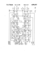
- FIGS. 3A and 3B are, in combination, a circuit schematic of a charging circuit suitable for use in the phase lock loop embodiment of FIG. 2.
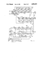
- FIG. 4 is a circuit schematic of a programmable bias circuit suitable for use in the frequency synthesizer embodiment of FIG. 1.
- a frequency synthesizer 10 may include at least one phase lock loop denoted as PLL 1.
- the synthesizer 10 is shown to include a plurality of phase lock loops further including the loops denoted as PLL 2 through PLL N. All of the phase lock loops of the frequency synthesizer 10 are of similar design and will be described herebelow in connection with the embodiment depicted by the functional block diagram schematic of FIG. 2.
- a common reference oscillator circuit 12 generates a very stable reference frequency signal REF which is provided commonly to the plurality of phase lock loops over signal line 14.
- a common bias circuit 16 is programmably operative to generate at least one bias reference signal which is coupled commonly to the plurality of phase lock loops.
- two bias reference signals are generated by the common bias circuit 16 and denoted as NBIAS and PBIAS which are coupled commonly to the phase lock loops over signal lines 18 and 20, respectively.
- a battery saving signal denoted as BATS is also commonly coupled to the phase lock loop circuits over a signal line 22.
- a central controller 24 which may be a programmed microcomputer system, for example, conducts coded digital words over a controller bus 26 and through an interface circuit 28 to be distributed commonly to all of the phase lock loop circuits over signal lines 30 and also to the common bias circuit over signal lines 32.
- the digitally coded words conducted over signal lines 30 and 32 may be of a parallel format, serial format, or a combination of both.
- a two-bit digital word is conducted over the signal lines 32 and stored in a storage register 34 for dynamically programming the common bias circuit 16.
- Signal lines CS1' and CS2' provide the status of the two bits of register 34 to the bias circuit 16 for setting the value of the bias reference signals which operation will be described in greater detail in connection with the embodiment depicted by the circuit schematic of FIG. 4.
- a two-bit digital word may be provided over the signal lines 30 to be dynamically programmed into a storage register 36 (see FIG. 2) of each of the phase lock loop circuits.
- 32 bits of data may be serially conducted over the signal lines 30 and stored in a 32-bit memory 38 (see FIG. 2) of each of the phase lock loop circuits.
- the aforementioned digital words of the signal line 30 are provided to the phase lock loop circuits for dynamically programming the synthesized frequency setting, loop bandwidth state, and frequency range thereof of each of the phase lock loop circuits. This will be described in greater detail hereinbelow.
- the battery saving signal 22 includes both sleep and awake cycles which are used to control the operations of the phase lock loops to reduce current drain on a battery source (not shown) during sleep cycles thereof.
- the phase lock loop circuits In response to the awake cycles of the battery saving signal 22, the phase lock loop circuits generate respective signals ON 1, ON 2, . . . , ON N which are conducted over signal lines 40 to the bias circuit 16 to likewise control the current drain thereof on the battery source.
- a suitable embodiment of a phase lock loop for use in the frequency synthesizer 10 of FIG. 1 will be described in connection with the functional block diagram schematic depicted in FIG. 2.
- the frequency signal conducted over signal line 14 is coupled to a divide by K divider network to develop a reference frequency signal which is conducted to a phase/frequency detector 44 over signal line 46.
- the value of K is programmed by a portion of the 32-bit word stored in the register 38. In the present embodiment, 11 bits are distributed to the network 42 over signal lines 48 for setting the value of K.
- a storage device 50 which includes a capacitive element 52 is disposed in the phase lock loop circuit for maintaining a voltage potential across the capacitive element 52.
- a signal representative of the voltage potential is conducted over signal line 54 to a voltage controlled oscillator 56 to govern the operation thereof.
- the oscillator 56 generates a synthesized frequency signal SF having a frequency proportional to the amplitude of the governing voltage signal 54.
- the synthesized frequency signal is conducted to an input of a divide by N frequency divider circuit 58 over signal line 60.
- the resultant frequency divided signal which will hereinafter be referred to as the feedback frequency signal is coupled to another input of the phase frequency detector 44 over signal line 62.
- the value of N of the frequency divider network 58 is set by a portion of the 32-bit digital word stored in the register 38. In the present embodiment, 19 bits of the 32-bit digital word are distributed to the circuit 58 over the signal lines 64 for setting the value of N.
- the phase detector 44 In response to the phase difference between the reference frequency signal 46 and feedback frequency signal 62, the phase detector 44 generates at least one control signal.
- the phase detector generates control signals denoted as NPU and NPD which are conducted over signal lines 66 and 68, respectively, to a charging circuit 70.
- the common bias reference signals of signal lines 18 and 20 are also conducted to the charging circuit 70.
- signals CS 1 and CS 2 representative of the status bits of the register 36 are also coupled to the charging circuit 70.
- the last two bits of the 32-bit digital word stored in register 38 are conducted to the charging circuit over signal lines 72 and may be used to set the loop bandwidth state of the phase lock loop as will be described in greater detail in connection with the embodiment depicted in FIG. 3A.
- the charging circuit 70 is coupled to the capacitive element 52 over signal line 74 to source and sink current to and from the capacitive element SW to adjust the voltage thereacross.
- the battery saving signal over signal line 22 may be coupled to the charging circuit 70 and also to a control input of a switch 76 which is coupled between the battery source denoted as Vs and the power supply input of the voltage control oscillator 56.
- switch 76 is opened to prevent current drain from the battery source for operation of the oscillator 56, and conversely, during awake cycles, the switch 76 is closed to power the oscillator 56 from the battery source Vs.
- the charging circuit 70 operates in response to the battery saving signal 22 to generate the signal ON over signal line 40 which is conducted to the common bias circuit 16 (see FIG. 1).
- the charging circuit 70 may be considered as divided into two parts, one being a logical control section and the other being an analog charging section.
- FIG. 3A depicts a suitable embodiment of the logical control section of the charging circuit 70.
- a section of the memory 38 containing the two bits of information which are conducted over signal lines 72 to the charging circuit 70 is depicted in FIG. 3A for completeness.
- D-type flip-flops 80 and 82 are included in the memory section 38 to store the two bits of data which govern the selection of the low and high loop bandwidth states (i.e. current levels).
- Control commands which are coupled over signal lines 30 from the central controller 24 via interface 28 include a serial data path SD for providing serial digital data to the D-type flip-flops of the section 38.
- complementary clocking signals SC and NSC are part of the signal lines 30 and used to clock the D-type flip-flops of the memory section 38 in order to store the serial digital data provided over line SD.
- a reset signal RST is provided as part of the control commands to reset the flip-flops of the memory section 38.
- the digital data bits 72 which set the loop bandwidth state (current levels) are conducted to corresponding D-type latches 84 and 86 of the charging circuit as depicted in FIG. 3A.
- the battery saver signal BATS over signal line 22 is coupled to a reset input of each of the latches 84 and 86.
- complementary clocking signals LC and NLC are coupled to the flip-flops 84 and 86 to provide control for the storage of the respective digital bits therein.
- the stored digital data bits of flip-flops 84 and 86 will hereinafter be referred to as Q1 and Q2, respectively, and their complements will hereinafter be referred to as Q1 and Q2.
- control signals NPU and NPD supplied from the phase detector 44 to govern the sourcing and sinking of current to the capacitive element 52 are coupled respectively through inverter gates 88 and 90 to one input of NAND gates 92 and 94, respectively.
- An auto bandwidth signal AUTBW is coupled through an inverter gate 96 to one input of another NAND gate 98.
- Another input of the NAND gate 98 is coupled to the signal line of Q2.
- the signal line of Q1 is coupled to one input of another NAND gate 100 which has another input thereof coupled to the output of the NAND gate 98.
- the signal lines of Q1 and Q2 are coupled to two inputs of a NAND gate 102, the output of which effecting the signal ON which is coupled through an inverter gate 104 to effect the complement NON thereof.
- the signal ON is coupled to the common bias circuit 16 for use therein as will be described in greater detail in connection with the embodiment of FIG. 4 herein below.
- the output of NAND gate 102 may also be coupled to another input of NAND gates 92 and 94.
- the output of NAND gate 94 is coupled through an inverter gate 106 to effect a control signal LBW and also coupled to one input of a NOR gate 108.
- the output of the NAND gate 100 is coupled to another input of the NOR gate 108 and to an input of another NOR gate 110.
- the output of the NAND gate 92 effects a control signal NLBW and is coupled to the other input of the NOR gate 110.
- the output of the NOR gate 110 is coupled through an inverter gate 112 to produce another control signal NHBW
- the output of the NOR gate 108 is coupled through a pair of cascaded inverter gates 114 and 116 to effect still another control signal HBW.
- the control signals NLBW, NHBW, HBW, and LBW are used in the charging circuit 70 to control MOSFET switches for the sourcing and sinking of current over signal line 74 to the storage capacitor 52 to adjust the voltage thereacross.
- MOSFET transistors are constructed in a circuit arrangement to form current mirrors which set the low and high current levels for the low loop bandwidth and high loop bandwidth phase lock loop states, respectively.
- the numbers shown alongside each of the MOSFET transistors represent their respective width over length ratios.
- the combination of MOSFET transistors 120, 122, 124, and 126 are coupled in tandem between the battery supply VDD and ground to effect a bias current I1 for the current mirrors of the current sourcing stages.
- the value of the sourcing bias current Il is set by a bias voltage NBIAS which is programmably generated by the common bias circuit 16 and applied to the gate of the transistor 124.
- the value of the bias current I2 is set by a bias voltage PBIAS which is also programmably generated by the common bias circuit 16 and applied to the gate of the transistor 130.
- a voltage Vg1 is produced at the drain of the diode configured MOSFET transistor 122 and is coupled to the gates of two MOSFET transistors 136 and 138 to produce a current mirroring effect thereat. That is, the sourcing current level conducted through transistor 136 is an amplification of the bias current Il based on the width to length ratios (gain relationship) of the transistors 122 and 136. In the present embodiment, this ratio was set at a value of 8 (low loop bandwidth state). Similarly, the sourcing current level conducted through the transistor 138 is also an amplification of the bias current I1 for the same reasons, and for the present embodiment, the amplification was set at 400 (high loop bandwidth state).
- a voltage Vg2 is effected at the source of the diode configured MOSFET transistor 132 in accordance with the value of the bias current I2.
- the voltage signal Vg2 is coupled to the gates of two MOSFET transistors 140 and 142 to produce the current mirroring effects (gain relationship) for the sinking current levels in both the low loop bandwidth and high loop bandwidth states as that described above for the transistors 136 and 138.
- the amplification settings for the transistors 140 and 142 are substantially the same as those set for transistors 136 and 138, respectively.
- MOSFET transistors 144 and 146 are coupled between the transistors 136 and 138, respectively, and the voltage supply VDD.
- the switches 144 and 146 are controlled by the respective signals NLBW and NHBW to conduct and not conduct low and high level sourcing current through the transistors 136 and 138, respectively.
- the coupled transistor pair 136 and 144 will be referred to as SW1
- the coupled pair of transistors 138 and 146 will be referred to as SW2.
- the MOSFET transistors 148 and 150 are coupled between their respective transistors 140 and 142 and ground potential.
- the transistors 148 and 150 are controlled by the signals LBW and HBW to conduct and not conduct low and high level sinking current through their respectively coupled transistors 140 and 142.
- the coupled pairs 140, 148 and 142, 150 will be referred to as SW3 and SW4, respectively.
- source current may be supplied to or drained from the capacitive element 52 via signal line 74 through SW1 and SW3 as controlled by the signals NLBW and LBW, respectively.
- sourcing current is supplied through both SW1 and SW2 and sinking current is conducted through SW3 and SW4 as controlled by the signals NHBW and HBW, respectively.
- the design is such that when both signals NHBW and NLBW are both logical 1's and signals LBW and HBW are both logical 0, all of the switches SW1, SW2, SW3, and SW4 are off, creating a floating state at the conduction line 74. This floating state may be created during a sleep cycle of the battery saving signal BATS in order to maintain the voltage across the capacitive element 52.
- the flip-flops 84 and 86 are reset which sets the signals Q1 and Q2 to a logical 1.
- the output of NAND gate 102 is effected to a logical 0 (i.e. the ON signal is set to logical 0) which disables the NAND gates 92 and 94 effecting a logical 1 at the outputs thereof.
- a plurality of switchable diode sections are included as part of the current mirror cirucits of the embodiment of the charging circuit 70 as shown in FIG. 3B.
- the combination of the programmable register 36, control signals CS1 and CS2, and the additional switchable diode sections of the mirror circuits comprise a digitally programmable control circuit for dynamically setting the frequency range of the selected loop bandwidth state in one of a predetermined plurality of frequency ranges.
- MOSFET transistors 160, 162, and 164 are configured as diodes and disposed in tandem with their respective switchable MOSFET transistors 166, 168, and 170 between the voltage supply bus VDD and the drain of MOSFET transistor 122.
- the switchable diode sections 160, 166; 162, 168; and 164, 170 are all in parallel with each other and in parallel with the non-switchable diode section comprising MOSFET transistors 120 and 122.
- MOSFET transistors 172, 174, and 176 are connected as diode elements in tandem with their respective MOSFET switches 178, 180, and 182 between ground potential and the source of MOSFET transistor 132.
- the switchable diode sections 172, 178; 174, 180; and 176, 182 are in parallel with each other and in parallel with the non-switchable diode section comprising MOSFET transistors 132 and 134.
- the plurality of switchable diode sections may be controlled by the programmed code of the digital signals CS1 and CS2 as decoded by a decoder circuit shown at 184. More specifically, the digital signal CS1 is coupled to an input of an inverter gate 186, to one input of a NOR gate 188 and to the gate of the MOSFET switch 170 over signal line denoted as L1 . The output of the inverter gate 186 is coupled to one input of a NOR gate 190 and also to the gate of the MOSFET switch 182 over a signal line denoted as L1. The digital signal CS2 is coupled to one input of both of the NOR gates 188 and 190.
- the output of the NOR gate 190 is coupled to the gate of the MOSFET switch 180 over a signal line denoted as L2 and also to the gate of the MOSFET switch 162 via an inverter gate 192 and a signal line denoted as L2.
- the output of the NOR gate 188 is coupled to the gate of the MOSFET switch 178 over a signal line denoted as L3 and also to the gate of the MOSFET switch 166 via an inverter gate 194 and a signal line denoted as L3.
- the switchable diode sections comprising the MOSFET switches 164, 170 and 176, 182 are switched concurrently to conduct and not conduct bias current therethrough by the signal L1 and its converse L1.
- the switchable diode sections comprising the MOSFET transistors 162, 168 and 174, 180 are controlled concurrently to conduct and not conduct bias current by the signals L2 and L2; and likewise, the switchable diode sections of 160, 166 and 172, 178 are controlled concurrently by the signals L3 and L3.
- the MOSFET transistors of the diode sections have a particular width to length ratio design as denoted by the ratios drafted alongside each transistor as depicted in the drawing of FIG. 3B.
- the principle of operation of the present embodiment is such that when a diode section is switched to conduct its respective bias current, the level of which being set by the voltage signals PBIAS and NBIAS, the width to length ratio of the conducting MOSFET transistors are additive to the width to length ratio of the MOSFET of its respective non-switching section to alter the gain relationship of its respective current mirror circuit to vary the current level of a selected loop bandwidth state for both of the current sourcing and sinking conditions.
- the sourcing switching diode sections 160 and 164 are switched on and the diode section 162 off and similarly, the sinking switchable diode sections 172 and 176 are conducted on and the switchable diode section 174 is switched off.
- the addition of their respective ratios yields a ratio of 32/20 which is in a 1:1 relationship with the low bandwidth state output sections yielding a gain relationship of unity for the low bandwidth state.
- the high bandwidth state will have a gain relationship with the bias current of approximately 50 times that of the low bandwidth state.
- the frequency range of the selected loop bandwidth state set by CS1, CS2 being 0,0, respectively is approximately 1/8 of the common frequency range set by the common bias circuit using the voltage values of the signals PBIAS and NBIAS.
- the other settable frequency ranges or gain relationships (the two being synonymous in the present embodiment) corresponding to the coded digital states of the signals CS1 and CS2 are shown in the truth table 2 found directly here below.
- FIG. 4 depicts a circuit schematic of a suitable embodiment for the bias circuit 16 which is programmably controlled by the digital word comprising, for the present embodiment, the digital signals CS1' and CS2' to dynamically set a common or maximum frequency range of the selected loop bandwidth state of at least one phase lock loop circuit (refer to the functional block diagram schematic of FIG. 1).
- a non-switchable diode section comprising MOSFET transistors 190 and 192 is coupled between the voltage supply VDD and the signal line 20.
- Another MOSFET transistor 194 is coupled between the signal line 20 and ground potential.
- another non-switchable diode section comprising the transistors 196 and 198 is coupled between ground potential and the signal line 18.
- a MOSFET transistor 200 is coupled between the voltage supply VDD and the signal line 18.
- the circuit arrangement 202 establishes very stable and fixed voltage levels at the gates of transistors 194 and 200 to fix the respective bias currents Ip and Ib therethrough for setting the voltage levels of the PBIAS and NBIAS bias reference signals. Accordingly, the common or maximum frequency range setting for the selected loop bandwidth state of the phase lock loops is commensurate with the voltage levels of the aforementioned bias reference signals as described hereabove in connection with FIG. 3B.
- the circuit arrangement 202 comprises a diode configured MOSFET transistor 204 coupled between the gate of transistor 194 and a resistor Rs which is coupled to ground potential.
- Another MOSFET transistor 206 is configured as a diode and coupled between the gate of transistor 200 and ground potential.
- Yet another diode configured MOSFET transistor 208 is coupled between the voltage supply VDD and the gate of transistor 200.
- a MOSFET transistor 210 is coupled between the voltage supply VDD and the gate of transistor 194. The gate of transistor 210 is coupled to the gate of transistor 200.
- a pair of MOSFET transistors 212 and 214 are coupled in tandem between the voltage supply VDD and ground potential.
- the gate of transistor 212 is coupled to the gate of transistor 200 and the gate of transistor 214 is coupled to the gate of transistor 194.
- Another pair of MOSFET transistors 216 and 218 are tandemly coupled between the voltage supply VDD and ground potential.
- Another MOSFET transistor 220 is coupled between VDD and the gate of transistor 200.
- Other MOSFET transistors 222 and 224 are coupled between the gate of transistor 200 and the node between the transistors 216 and 218 and between the drain of transistor 200 and ground potential, respectively.
- Still another MOSFET transistor 226 is coupled between the gate of transistor 194 and ground potential.
- the gate of transistor 222 is coupled to he node connection between transistors 212 and 214 and also to a capacitor C1 which is coupled to ground potential.
- the value of capacitor C1 may be on the order of 50 pf for the present embodiment.
- the gate of transistor 226 is also coupled to the node connection between transistors 216 and 218.
- the gates of transistors 216, 218, and 220 are commonly coupled to the output of an inverter gate 228.
- the output of a NOR gate 230 is coupled to the gate of transistor 224 and also to the input of the inverter gate 228.
- the "ON" signals generated from the phase lock loop circuits are coupled to respective inputs of the NOR gate 230.
- a bias current I3 is established through the diode section 204 by the value of the resistor Rs.
- This bias current sets a voltage Vg3 at the gates of transistors 194 and 214.
- Transistor 212 establishes a drain current such that there exists a voltage swing applied to the gate of transistor 222 as a result of the voltage gain between the transistors 214 and 204.
- the voltage at the gate of transistor 222 is translated into another bias current conducted through the diode section 208 and which is mirrored through the transistor stages 210 and 212 in accordance with the gain relationship with transistor 208.
- the current conducted through the transistor 210 and 212 feed the transistor sections 204 and 214 which provides a positive feedback that stabilizes at a point where the total voltage across the transistor 204 and resistor Rs is equal to the total voltage across the transistor 214 to ground.
- the capacitance C1 provides filtering to stabilize the positive feedback loop and keep it from going into oscillation.
- the bias current I3 be set at approximately 10 ⁇ A such that due to the current mirror relationships, the bias currents Ip and Ib through the transistors 194 and 200, respectively, will stabilize at approximately 1 ⁇ A each.
- the width to length design ratios of the MOSFET transistors are shown alongside each in the drawing of FIG. 4.
- the bias circuit 16 is deactivated. More specifically, the output of the NOR gate 230 is set to a logical 1 which causes the output of the inverter gate 228 to be set to a logical 0. Under these conditions, the transistors 216, 220, and 224 are caused to be shorted and the transistors 218, 222, and 226 are caused to be blocked. In response, the signal line 18 is brought to ground through the transistor 224 and since the transistor 194 is blocked by the shorting of transistor 210, the signal line 20 is allowed to be pulled up to the supply voltage VDD by the diode section 190, 192. Consequently, with the signal line 20 at VDD and the signal line 18 at ground potential, the charging circuits 70 of the phase lock loop circuits are effected to their floating states to maintain the voltage across the capacitive element 52.
- a plurality of diode sections are coupled between the supply voltage VDD and the signal line 20 and also between the signal line 18 and ground potential.
- the switchable diode sections may be dynamically switched in accordance with the programmed code of the digital signal CS1' and CS2' to set the voltage of the NBIAS and PBIAS signals which establish a common or maximum frequency range for the selected loop bandwidth state of all of the phase lock loop circuits.
- tandemly coupled pairs of MOSFET transistors 232, 234; 236, 238; and 240, 242 are configured in parallel with each other and in parallel with the non-switchable diode section 190, 192 between the voltage supply VDD and the signal line 20.
- tandemly coupled MOSFET transistors 244, 246; 248, 250; and 252, 254 are coupled in parallel together and with the non-switchable diode section 196, 198 between the signal line 18 and ground potential.
- a decoder circuit 256 is provided in the bias circuit for decoding the digital codes of the signals CS1' and CS2' to permit a corresponding selection of the plurality of diode sections to establish the corresponding voltage level desired at the signal lines 18 and 20. More specifically, the digital signal CS2' is coupled to one input of a NOR gate 260, to the gate of the switching transistor 240 over a signal line denoted as L1 and also to the gate of the switching transistor 254 through an inverter gate 262 and over a signal line denoted as L1. In addition, the digital signal CS1' is coupled to another input of the NOR gate 260 and to one input of another NOR gate 264.
- the output of the inverter gate 262 is coupled to another input of the NOR gate 264.
- the output of the NOR gate 264 is coupled to the gate of the switching transistor 250 over a signal line denoted as L2 and also to the gate of the switching transistor 236 through an inverter gate 266 and over a signal line denoted as L2.
- the output of the NOR gate 260 is coupled to the gate of the switching transistor 246 over a signal line denoted as L3 and also to the gate of the switching transistor 232 through an inverter 268 and over a signal line denoted as L3.
- the decoded switching signal and its complement concurrently controls the corresponding diode section.
- L1 and L1 concurrently control the diode section 240, 242 and the diode section 252, 254 to source and sink bias current set by the transistors 194 and 200, respectively.
- the voltage levels set for the PBIAS and NBIAS bias reference signals are substantially the same.
- the programmable control operation of the bias circuit 16 may be shown by a truth table such as that found in the truth table 3 shown here below.
- the central controller 24 may set a new individual frequency channel setting for each of the phase lock loops 1 through N by dynamically programming a serialized digital word (via the interface 28 and signal lines 30) in each of the storage registers 38 thereof.
- the particular loop bandwidth state may also be set by the central controller 24 within the serialized digital data word based on the new frequency channel setting for each phase lock loop.
- the programmed digital word of the storage register 38 is distributed to the appropriate circuits as described in connection with the embodiment of FIG. 2 to set the new frequency channel setting and new loop bandwidth state utilizing the signal lines 48, 64, and 72.
- the central controller 24 may also set a common or maximum frequency for the selected loop bandwidth states of all of the phase lock loops by dynamically programming a digitally coded word (via the interface 28 and signal lines 32) in the storage register 34.
- the resulting digital signals CS1' and CS2' control the bias circuit as described hereabove in connection with the embodiment of FIG. 4 to establish the appropriate voltage levels for the bias reference signals NBIAS and PBIAS which are conducted to the charging circuits 70 of the various phase lock loop circuits to govern the setting of the common or maximum current levels therein as described in connection with the embodiment of FIG. 3B.
- the central controller 24 may also dynamically program the individual frequency ranges of the selected loop bandwidth states of the various phase lock loops by conducting individual two-bit coded words CS1, CS2 over the signal lines 30 to each of the phase lock loops for storage in the register 36 thereof.
- the resulting digital states of the signals CS1 and CS2 control the plurality of diode sections within each of the charging circuits 70 of the various phase lock loops to govern dynamically and individually the setting of the frequency range of the selected loop bandwidth state thereof.
Abstract
Description
                                  TRUTH TABLE 1
__________________________________________________________________________
A Q1
    Q2
      NPU
         NPD
            LBW HBW NLBW
                        NHBW SW1
                                SW2
                                   SW3
                                      SW4
__________________________________________________________________________
X 1 0 1  0  1   1   1   1    OFF
                                OFF
                                   ON ON
X 0 X 1  0  1   0   1   1    OFF
                                OFF
                                   ON OFF
1 1 1 1  0  1   1   1   1    OFF
                                OFF
                                   ON ON
0 1 1 1  0  1   0   1   1    OFF
                                OFF
                                   ON OFF
X 1 0 0  1  0   0   0   0    ON ON OFF
                                      OFF
X 0 X 0  1  0   0   0   1    ON OFF
                                   OFF
                                      OFF
1 1 1 0  1  0   0   0   0    ON ON OFF
                                      OFF
0 1 1 0  1  0   0   0   1    ON OFF
                                   OFF
                                      OFF
__________________________________________________________________________
              TRUTH TABLE 2
______________________________________
                                    Gain
                                    Relationship
CS1  CS2      L1,L1.sup.----
                      L2,L2.sup.----
                              L3,L3.sup.----
                                    (LBW)
______________________________________
0    0        ON      OFF     ON    X1
1    0        OFF     ON      OFF   X2
0    1        ON      OFF     OFF   X4
1    1        OFF     OFF     OFF   X8
______________________________________
              TRUTH TABLE 3
______________________________________
                                    Bias Voltage
CS1  CS2      L1,L1.sup.----
                      L2,L2.sup.----
                              L3,L3.sup.----
                                    Level
______________________________________
1    1        OFF     OFF     OFF   1
1    0        ON      OFF     OFF   1/2
0    1        OFF     ON      OFF   1/4
0    0        ON      OFF     ON    1/8
______________________________________
Claims (15)
Priority Applications (2)
| Application Number | Priority Date | Filing Date | Title |
|---|---|---|---|
| US07/345,809 US4901033A (en) | 1989-05-01 | 1989-05-01 | Frequency synthesizer with dynamically programmable frequency range of selected loop bandwith |
| PCT/US1990/002042 WO1990013948A1 (en) | 1989-05-01 | 1990-04-16 | Frequency synthesizer with dynamically programmable frequency range of selected loop bandwidth |
Applications Claiming Priority (1)
| Application Number | Priority Date | Filing Date | Title |
|---|---|---|---|
| US07/345,809 US4901033A (en) | 1989-05-01 | 1989-05-01 | Frequency synthesizer with dynamically programmable frequency range of selected loop bandwith |
Publications (1)
| Publication Number | Publication Date |
|---|---|
| US4901033A true US4901033A (en) | 1990-02-13 |
Family
ID=23356577
Family Applications (1)
| Application Number | Title | Priority Date | Filing Date |
|---|---|---|---|
| US07/345,809 Expired - Lifetime US4901033A (en) | 1989-05-01 | 1989-05-01 | Frequency synthesizer with dynamically programmable frequency range of selected loop bandwith |
Country Status (2)
| Country | Link |
|---|---|
| US (1) | US4901033A (en) |
| WO (1) | WO1990013948A1 (en) |
Cited By (14)
| Publication number | Priority date | Publication date | Assignee | Title |
|---|---|---|---|---|
| EP0461358A1 (en) * | 1990-06-15 | 1991-12-18 | Mitsubishi Denki Kabushiki Kaisha | Frequency synthesizer |
| US5128632A (en) * | 1991-05-16 | 1992-07-07 | Motorola, Inc. | Adaptive lock time controller for a frequency synthesizer and method therefor |
| US5140284A (en) * | 1991-02-20 | 1992-08-18 | Telefonaktiebolaget L M Ericsson | Broad band frequency synthesizer for quick frequency retuning |
| EP0627820A2 (en) * | 1993-06-02 | 1994-12-07 | Motorola, Inc. | A charge pump with a programmable pump current and system |
| US5422911A (en) * | 1993-09-17 | 1995-06-06 | Motorola, Inc. | Frequency walled phase lock loop |
| WO1995017043A1 (en) * | 1993-12-17 | 1995-06-22 | Motorola Inc. | Apparatus and method for controlling the loop bandwidth of a phase locked loop |
| US5498998A (en) * | 1992-11-16 | 1996-03-12 | Gehrke; James K. | Method for adjusting the output frequency of a frequency synthesizer |
| US5631587A (en) * | 1994-05-03 | 1997-05-20 | Pericom Semiconductor Corporation | Frequency synthesizer with adaptive loop bandwidth |
| US5751175A (en) * | 1995-01-30 | 1998-05-12 | Nec Corporation | Control of clock signal in semiconductor device |
| US6094236A (en) * | 1996-04-26 | 2000-07-25 | Kabushiki Kaisha Toshiba | Tuner circuit |
| US6310927B1 (en) * | 1994-03-31 | 2001-10-30 | Stmicroelectronics, Inc. | First order tuning circuit for a phase-locked loop |
| US20070127616A1 (en) * | 2005-12-02 | 2007-06-07 | Altera Corporation | Programmable transceivers that are able to operate over wide frequency ranges |
| US20080159361A1 (en) * | 2006-12-29 | 2008-07-03 | Nokia Corporation | Dynamically adjusted phase locked loop |
| CN100437676C (en) * | 2003-09-26 | 2008-11-26 | 恩益禧电子股份有限公司 | Differential ab class amplifier circuit and drive circuit using the same |
Citations (4)
| Publication number | Priority date | Publication date | Assignee | Title |
|---|---|---|---|---|
| US4167711A (en) * | 1978-05-26 | 1979-09-11 | Motorola, Inc. | Phase detector output stage for phase locked loop |
| US4659999A (en) * | 1983-10-31 | 1987-04-21 | Anritsu Electric Company Limited | Direct frequency synthesizer which is step-wise variable and has phase continuity and phase reproducibility when switching frequencies |
| US4745372A (en) * | 1985-10-17 | 1988-05-17 | Matsushita Electric Industrial Co., Ltd. | Phase-locked-loop circuit having a charge pump |
| US4771249A (en) * | 1987-05-26 | 1988-09-13 | Motorola, Inc. | Phase locked loop having a filter with controlled variable bandwidth |
-
1989
- 1989-05-01 US US07/345,809 patent/US4901033A/en not_active Expired - Lifetime
-
1990
- 1990-04-16 WO PCT/US1990/002042 patent/WO1990013948A1/en unknown
Patent Citations (4)
| Publication number | Priority date | Publication date | Assignee | Title |
|---|---|---|---|---|
| US4167711A (en) * | 1978-05-26 | 1979-09-11 | Motorola, Inc. | Phase detector output stage for phase locked loop |
| US4659999A (en) * | 1983-10-31 | 1987-04-21 | Anritsu Electric Company Limited | Direct frequency synthesizer which is step-wise variable and has phase continuity and phase reproducibility when switching frequencies |
| US4745372A (en) * | 1985-10-17 | 1988-05-17 | Matsushita Electric Industrial Co., Ltd. | Phase-locked-loop circuit having a charge pump |
| US4771249A (en) * | 1987-05-26 | 1988-09-13 | Motorola, Inc. | Phase locked loop having a filter with controlled variable bandwidth |
Non-Patent Citations (1)
| Title |
|---|
| Specification for NJ88C31, Plessey Co. Pfc, Publication No. PS 2059, May 1986. * |
Cited By (20)
| Publication number | Priority date | Publication date | Assignee | Title |
|---|---|---|---|---|
| EP0461358A1 (en) * | 1990-06-15 | 1991-12-18 | Mitsubishi Denki Kabushiki Kaisha | Frequency synthesizer |
| US5140284A (en) * | 1991-02-20 | 1992-08-18 | Telefonaktiebolaget L M Ericsson | Broad band frequency synthesizer for quick frequency retuning |
| US5128632A (en) * | 1991-05-16 | 1992-07-07 | Motorola, Inc. | Adaptive lock time controller for a frequency synthesizer and method therefor |
| US5498998A (en) * | 1992-11-16 | 1996-03-12 | Gehrke; James K. | Method for adjusting the output frequency of a frequency synthesizer |
| EP0627820A2 (en) * | 1993-06-02 | 1994-12-07 | Motorola, Inc. | A charge pump with a programmable pump current and system |
| EP0627820A3 (en) * | 1993-06-02 | 1994-12-14 | Motorola, Inc. | A charge pump with a programmable pump current and system |
| US5422911A (en) * | 1993-09-17 | 1995-06-06 | Motorola, Inc. | Frequency walled phase lock loop |
| CN1035584C (en) * | 1993-12-17 | 1997-08-06 | 摩托罗拉公司 | Apparatus and method for controlling the loop bandwidth of a phase locked loop |
| GB2290186A (en) * | 1993-12-17 | 1995-12-13 | Motorola Inc | Apparatus and method for controlling the loop bandwidth of a phase locked loop |
| WO1995017043A1 (en) * | 1993-12-17 | 1995-06-22 | Motorola Inc. | Apparatus and method for controlling the loop bandwidth of a phase locked loop |
| US5703539A (en) * | 1993-12-17 | 1997-12-30 | Motorola, Inc. | Apparatus and method for controlling the loop bandwidth of a phase locked loop |
| GB2290186B (en) * | 1993-12-17 | 1998-08-05 | Motorola Inc | Apparatus and method for controlling the loop bandwidth of a phase locked loop |
| US6310927B1 (en) * | 1994-03-31 | 2001-10-30 | Stmicroelectronics, Inc. | First order tuning circuit for a phase-locked loop |
| US5631587A (en) * | 1994-05-03 | 1997-05-20 | Pericom Semiconductor Corporation | Frequency synthesizer with adaptive loop bandwidth |
| US5751175A (en) * | 1995-01-30 | 1998-05-12 | Nec Corporation | Control of clock signal in semiconductor device |
| US6094236A (en) * | 1996-04-26 | 2000-07-25 | Kabushiki Kaisha Toshiba | Tuner circuit |
| CN100437676C (en) * | 2003-09-26 | 2008-11-26 | 恩益禧电子股份有限公司 | Differential ab class amplifier circuit and drive circuit using the same |
| US20070127616A1 (en) * | 2005-12-02 | 2007-06-07 | Altera Corporation | Programmable transceivers that are able to operate over wide frequency ranges |
| US7539278B2 (en) * | 2005-12-02 | 2009-05-26 | Altera Corporation | Programmable transceivers that are able to operate over wide frequency ranges |
| US20080159361A1 (en) * | 2006-12-29 | 2008-07-03 | Nokia Corporation | Dynamically adjusted phase locked loop |
Also Published As
| Publication number | Publication date |
|---|---|
| WO1990013948A1 (en) | 1990-11-15 |
Similar Documents
| Publication | Publication Date | Title |
|---|---|---|
| US4926141A (en) | Frequency synthesizer with improved automatic control of loop bandwidth selection | |
| US4893094A (en) | Frequency synthesizer with control of start-up battery saving operations | |
| US4901033A (en) | Frequency synthesizer with dynamically programmable frequency range of selected loop bandwith | |
| US5272453A (en) | Method and apparatus for switching between gain curves of a voltage controlled oscillator | |
| KR100341943B1 (en) | Charge pumps and systems with them | |
| US6420914B1 (en) | Charge pump circuit having switching circuits for reducing leakage currents | |
| US5128632A (en) | Adaptive lock time controller for a frequency synthesizer and method therefor | |
| KR100806117B1 (en) | Phase-locked-loop circuit having voltage-controlled-oscillator and method of controlling the same | |
| JPH09214338A (en) | Pll frequency synthesizer | |
| US6670833B2 (en) | Multiple VCO phase lock loop architecture | |
| US5847614A (en) | Low power charge pump | |
| US6163184A (en) | Phase locked loop (PLL) circuit | |
| US7151413B2 (en) | Low noise charge pump for PLL-based frequence synthesis | |
| US5285114A (en) | Phase lock loop charge pump with symmetrical charge and discharge currents | |
| US6107889A (en) | Phase locked loop charge pump circuit | |
| USRE36874E (en) | Supply voltage tolerant phase-locked loop circuit | |
| JP3609658B2 (en) | PLL circuit | |
| US7446595B2 (en) | Charge pump circuit with power management | |
| EP2984758A1 (en) | Phase locked loop and method for operating the same | |
| JP3614778B2 (en) | Oscillator circuit with crystal oscillator | |
| KR20060008412A (en) | Fast locking charge pump phase locked loop and fast locking charge pumping method for the same | |
| JP4219669B2 (en) | Constant voltage generation circuit and PLL circuit | |
| US7123065B1 (en) | Method of improving lock acquisition times in systems with a narrow frequency range | |
| JP3562189B2 (en) | Charge pump circuit | |
| KR20090054517A (en) | Voltage divider having output level depending on a frequency and pll having the same |
Legal Events
| Date | Code | Title | Description |
|---|---|---|---|
| AS | Assignment |
Owner name: MOTOROLA, INC., ILLINOIS Free format text: ASSIGNMENT OF ASSIGNORS INTEREST.;ASSIGNORS:HEROLD, BARRY W.;TAHERNIA, OMID;REEL/FRAME:005181/0183;SIGNING DATES FROM 19890427 TO 19891107 |
|
| STCF | Information on status: patent grant |
Free format text: PATENTED CASE |
|
| FEPP | Fee payment procedure |
Free format text: PAYOR NUMBER ASSIGNED (ORIGINAL EVENT CODE: ASPN); ENTITY STATUS OF PATENT OWNER: LARGE ENTITY |
|
| FPAY | Fee payment |
Year of fee payment: 4 |
|
| FPAY | Fee payment |
Year of fee payment: 8 |
|
| FPAY | Fee payment |
Year of fee payment: 12 |
|
| AS | Assignment |
Owner name: FREESCALE SEMICONDUCTOR, INC., TEXAS Free format text: ASSIGNMENT OF ASSIGNORS INTEREST;ASSIGNOR:MOTOROLA, INC.;REEL/FRAME:015698/0657 Effective date: 20040404 Owner name: FREESCALE SEMICONDUCTOR, INC.,TEXAS Free format text: ASSIGNMENT OF ASSIGNORS INTEREST;ASSIGNOR:MOTOROLA, INC.;REEL/FRAME:015698/0657 Effective date: 20040404 |
|
| AS | Assignment |
Owner name: CITIBANK, N.A. AS COLLATERAL AGENT, NEW YORK Free format text: SECURITY AGREEMENT;ASSIGNORS:FREESCALE SEMICONDUCTOR, INC.;FREESCALE ACQUISITION CORPORATION;FREESCALE ACQUISITION HOLDINGS CORP.;AND OTHERS;REEL/FRAME:018855/0129 Effective date: 20061201 Owner name: CITIBANK, N.A. AS COLLATERAL AGENT,NEW YORK Free format text: SECURITY AGREEMENT;ASSIGNORS:FREESCALE SEMICONDUCTOR, INC.;FREESCALE ACQUISITION CORPORATION;FREESCALE ACQUISITION HOLDINGS CORP.;AND OTHERS;REEL/FRAME:018855/0129 Effective date: 20061201 |
|
| AS | Assignment |
Owner name: FREESCALE SEMICONDUCTOR, INC., TEXAS Free format text: PATENT RELEASE;ASSIGNOR:CITIBANK, N.A., AS COLLATERAL AGENT;REEL/FRAME:037354/0225 Effective date: 20151207 |