US4901041A - High-performance package for monolithic microwave integrated circuits - Google Patents
High-performance package for monolithic microwave integrated circuits Download PDFInfo
- Publication number
- US4901041A US4901041A US07/251,446 US25144688A US4901041A US 4901041 A US4901041 A US 4901041A US 25144688 A US25144688 A US 25144688A US 4901041 A US4901041 A US 4901041A
- Authority
- US
- United States
- Prior art keywords
- feedthrough
- transmission line
- signal conductor
- pseudostrip
- microstrip
- Prior art date
- Legal status (The legal status is an assumption and is not a legal conclusion. Google has not performed a legal analysis and makes no representation as to the accuracy of the status listed.)
- Expired - Lifetime
Links
- 239000004020 conductor Substances 0.000 claims abstract description 30
- 230000005540 biological transmission Effects 0.000 claims abstract description 29
- 238000000034 method Methods 0.000 claims abstract description 17
- 238000007789 sealing Methods 0.000 claims abstract description 15
- 239000003989 dielectric material Substances 0.000 claims description 4
- 230000007704 transition Effects 0.000 claims 5
- 238000001465 metallisation Methods 0.000 abstract description 17
- 238000013461 design Methods 0.000 abstract description 8
- 229910052751 metal Inorganic materials 0.000 abstract description 6
- 239000002184 metal Substances 0.000 abstract description 6
- 238000005219 brazing Methods 0.000 abstract description 3
- 238000007639 printing Methods 0.000 abstract description 2
- 239000000919 ceramic Substances 0.000 description 13
- 238000004519 manufacturing process Methods 0.000 description 6
- 239000010409 thin film Substances 0.000 description 5
- 239000010408 film Substances 0.000 description 4
- 238000005516 engineering process Methods 0.000 description 3
- 238000002955 isolation Methods 0.000 description 3
- 238000004806 packaging method and process Methods 0.000 description 3
- PXHVJJICTQNCMI-UHFFFAOYSA-N Nickel Chemical compound [Ni] PXHVJJICTQNCMI-UHFFFAOYSA-N 0.000 description 2
- 238000010923 batch production Methods 0.000 description 2
- 239000011521 glass Substances 0.000 description 2
- 239000000463 material Substances 0.000 description 2
- 230000008569 process Effects 0.000 description 2
- 229910018404 Al2 O3 Inorganic materials 0.000 description 1
- 229910017083 AlN Inorganic materials 0.000 description 1
- PNEYBMLMFCGWSK-UHFFFAOYSA-N Alumina Chemical compound [O-2].[O-2].[O-2].[Al+3].[Al+3] PNEYBMLMFCGWSK-UHFFFAOYSA-N 0.000 description 1
- 229910015363 Au—Sn Inorganic materials 0.000 description 1
- 229910001080 W alloy Inorganic materials 0.000 description 1
- 238000013459 approach Methods 0.000 description 1
- 230000008901 benefit Effects 0.000 description 1
- LTPBRCUWZOMYOC-UHFFFAOYSA-N beryllium oxide Inorganic materials O=[Be] LTPBRCUWZOMYOC-UHFFFAOYSA-N 0.000 description 1
- 239000003990 capacitor Substances 0.000 description 1
- SBYXRAKIOMOBFF-UHFFFAOYSA-N copper tungsten Chemical compound [Cu].[W] SBYXRAKIOMOBFF-UHFFFAOYSA-N 0.000 description 1
- 230000008878 coupling Effects 0.000 description 1
- 238000010168 coupling process Methods 0.000 description 1
- 238000005859 coupling reaction Methods 0.000 description 1
- 230000009977 dual effect Effects 0.000 description 1
- 230000005496 eutectics Effects 0.000 description 1
- PCHJSUWPFVWCPO-UHFFFAOYSA-N gold Chemical compound [Au] PCHJSUWPFVWCPO-UHFFFAOYSA-N 0.000 description 1
- 229910052737 gold Inorganic materials 0.000 description 1
- 239000010931 gold Substances 0.000 description 1
- 230000006872 improvement Effects 0.000 description 1
- 238000003780 insertion Methods 0.000 description 1
- 230000037431 insertion Effects 0.000 description 1
- 229910000833 kovar Inorganic materials 0.000 description 1
- 230000008018 melting Effects 0.000 description 1
- 238000002844 melting Methods 0.000 description 1
- 238000012986 modification Methods 0.000 description 1
- 230000004048 modification Effects 0.000 description 1
- 229910052759 nickel Inorganic materials 0.000 description 1
- 238000007747 plating Methods 0.000 description 1
- 230000000717 retained effect Effects 0.000 description 1
- WFKWXMTUELFFGS-UHFFFAOYSA-N tungsten Chemical compound [W] WFKWXMTUELFFGS-UHFFFAOYSA-N 0.000 description 1
- 229910052721 tungsten Inorganic materials 0.000 description 1
- 239000010937 tungsten Substances 0.000 description 1
Images
Classifications
-
- H—ELECTRICITY
- H01—ELECTRIC ELEMENTS
- H01P—WAVEGUIDES; RESONATORS, LINES, OR OTHER DEVICES OF THE WAVEGUIDE TYPE
- H01P1/00—Auxiliary devices
- H01P1/20—Frequency-selective devices, e.g. filters
- H01P1/201—Filters for transverse electromagnetic waves
- H01P1/203—Strip line filters
- H01P1/2039—Galvanic coupling between Input/Output
-
- H—ELECTRICITY
- H01—ELECTRIC ELEMENTS
- H01L—SEMICONDUCTOR DEVICES NOT COVERED BY CLASS H10
- H01L23/00—Details of semiconductor or other solid state devices
- H01L23/58—Structural electrical arrangements for semiconductor devices not otherwise provided for, e.g. in combination with batteries
- H01L23/64—Impedance arrangements
- H01L23/66—High-frequency adaptations
-
- H—ELECTRICITY
- H01—ELECTRIC ELEMENTS
- H01P—WAVEGUIDES; RESONATORS, LINES, OR OTHER DEVICES OF THE WAVEGUIDE TYPE
- H01P5/00—Coupling devices of the waveguide type
- H01P5/08—Coupling devices of the waveguide type for linking dissimilar lines or devices
- H01P5/085—Coaxial-line/strip-line transitions
-
- H—ELECTRICITY
- H01—ELECTRIC ELEMENTS
- H01L—SEMICONDUCTOR DEVICES NOT COVERED BY CLASS H10
- H01L2924/00—Indexing scheme for arrangements or methods for connecting or disconnecting semiconductor or solid-state bodies as covered by H01L24/00
- H01L2924/0001—Technical content checked by a classifier
- H01L2924/0002—Not covered by any one of groups H01L24/00, H01L24/00 and H01L2224/00
-
- H—ELECTRICITY
- H01—ELECTRIC ELEMENTS
- H01L—SEMICONDUCTOR DEVICES NOT COVERED BY CLASS H10
- H01L2924/00—Indexing scheme for arrangements or methods for connecting or disconnecting semiconductor or solid-state bodies as covered by H01L24/00
- H01L2924/095—Indexing scheme for arrangements or methods for connecting or disconnecting semiconductor or solid-state bodies as covered by H01L24/00 with a principal constituent of the material being a combination of two or more materials provided in the groups H01L2924/013 - H01L2924/0715
- H01L2924/097—Glass-ceramics, e.g. devitrified glass
- H01L2924/09701—Low temperature co-fired ceramic [LTCC]
-
- H—ELECTRICITY
- H01—ELECTRIC ELEMENTS
- H01L—SEMICONDUCTOR DEVICES NOT COVERED BY CLASS H10
- H01L2924/00—Indexing scheme for arrangements or methods for connecting or disconnecting semiconductor or solid-state bodies as covered by H01L24/00
- H01L2924/30—Technical effects
- H01L2924/301—Electrical effects
- H01L2924/3011—Impedance
Definitions
- the present invention relates generally to packaging for integrated circuits, and, more specifically, to high-performance packaging for monolithic microwave integrated circuits (MMICs) operable at frequencies in the 20 GHz range.
- MMICs monolithic microwave integrated circuits
- Packaging techniques known to the prior art have been well documented.
- Known manufacturing techniques include cofired ceramic enclosures using thick-film metallization, glass-sealed ceramic enclosures using thin-film metallization, metal enclosures having ceramic feedthroughs, and metal enclosures having glass feedthroughs.
- ceramic-package manufacture is a batch process, it has a distinct advantage over some of the other technologies available. If the yield of the process is high, ceramic packages should be low cost in reasonable volume.
- An MMIC package capable of good performance in the 20 GHz range should have low insertion loss and voltage standing wave ratio (VSWR) per lead feedthrough, good isolation between leads, microstrip compatibility, and an electrical design approach extendable to higher frequencies.
- the present invention fulfills all of these goals in a package that is cascadable, bondable, and capable of extensive application throughout the entire MMIC industry, including military applications.
- the present invention incorporates a specially-designed low-pass filter into the feedthrough itself to provide compensation for discrepancies from the impedance required for an MMIC package to be matched to a transmission line (typically 50 Ohms).
- the compensation used is similar to LC techniques known to the prior art, but allows all parameters to be adjusted and the complete filter to be printed.
- the main features of the present compensated feedthrough include minimum width for the under-wall conductor and brazing metallization, two open-circuited stubs at the package-die interface for wire bonding ease, and metal-filled vias connecting the ground plane base and the lid sealing ring to bring the lid sealing ring to RF ground.
- the present invention also includes a method for designing the desired feedthrough that obviates the need for scale-model feedthrough design before printing, a prior art method that requires precision in the scale model.
- An electrical model of a feedthrough is first derived.
- the electrical model is then adjusted according to the parameters desired for a new, compensated feedthrough using any known method, including software such as Touchstone. Finally, the new feedthrough is fabricated based upon the adjusted electrical model.
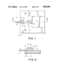
- FIG. 1 is a plan view of a compensated feedthrough fabricated in accordance with the teachings of the present invention
- FIG. 2 is a cross section taken along the line II--II of the feedthrough shown in FIG. 1;
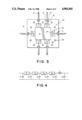
- FIG. 3 is a plan view of an integrated circuit package fabricated in accordance with the teachings of the present invention.
- FIG. 4 is an equivalent circuit for feedthrough of the type shown in FIG. 2.
- FIG. 1 is a plan view of a preferred embodiment of the compensated feedthrough constructed in accordance with the present invention.
- the main features of the feedthrough include the conductor under-wall width, which is reduced to the minimum that can be printed reproducibly in thick-film technology (currently about 6 mil); the brazing-metallization width, which is likewise reduced to the minimum allowable; two open-circuited stubs set immediately prior to the interface between the feedthrough and the die; and a plurality of metal-filled vias formed in the ceramic to connect the ground plane base to the lid sealing ring.
- the feedthrough conducts a signal between the exterior of an electronics package (designated generally by reference numeral 2) and an integrated circuit chip located in die cavity 4.
- the integrated circuit chip in this preferred embodiment is a monolithic microwave integrated circuit (MMIC) that operates at frequencies as high as 20 GHz, although the invention could conceivably be applied to electronic circuit packages that utilize other known integrated circuits.
- MMIC monolithic microwave integrated circuit
- the present compensated feedthrough includes first microstrip transmission line section 6, transmission line section 16, and second microstrip transmission line section 22.
- microstrip section 6 may connnect to an external transmission line (e.g., coaxial) via pin lead 8 as shown, or, alternatively, via any input known to the art, including a surface mount input.
- microstrip section 6 includes metallization 10 forming a signal conductor on dielectric layer 12 using known techniques.
- Transmission line section 16 comprises metallization 10 forming a signal conductor plated between dielectric layers 12 and 18, ground plane base 14, and upper sealing ring 20, which is formed over second dielectric layer 18 using known techniques. As shown in FIG. 1, metallization 10 is narrowed, or “necked down", when it passes below second dielectric layer 18 ("under-wall"). Section 16, which resembles stripline or RIPLATETM, is nevertheless not pure stripline since lid sealing ring 20 is not a true RF ground. Therefore, section 16 may be referred to as a pseudostrip section of transmission line, and analyzed accordingly.
- Second microstrip transmission line section 22 which is similar to microstrip section 6, terminates in bond pad 24, formed substantially square, of metallization layer 10 just before die cavity 4.
- Bond pad 24 is well known in the art as effecting two open-circuited stubs, which are modeled as a shunt capacitance. Bond pad 24 also enhances wire bonding to the MMIC.
- a plurality of apertures, or vias, 26 are formed in the package.
- Vias 26 extend from ground plane base 14 up through the dielectric material to lid sealing ring 20, and are filled with metal to bring lid sealing ring 20 substantially to RF ground.
- vias 26 represent an improvement over prior art packages, which rely solely upon metallization of the internal walls of the package to reference the lid sealing ring. While internal wall metallization is preferably retained in the present IC package, vias 26 both improve the status of lid sealing ring 20 as RF ground and greatly improve isolation between leads, which could not be accomplished simply by metallizing the internal walls.
- FIG. 3 illustrates a representative package incorporating six feedthroughs having the compensation described with respect to FIG. 1, with like reference numerals designating like elements.
- vias 26 are preferably spaced approximately equidistantly between the various feedthroughs that are located in the waveguide portion 28 of the package. As many or as few vias as are desired may be provided in the package up to the limits of manufacturing technology. The more vias, the better the isolation.
- the feedthrough design described above is based on a low-pass filter consisting of the lead-attachment area, the microstrip-pseudostrip-microstrip transmission line, and the dual open-circuited stubs.
- low-pass filters have been used in the prior art to provide compensation at the feedthrough, the present invention allows, within manufacturability limits, all parameters to be adjusted, and the complete filter to be printed.
- One way to establish a desired electrical model is to begin with an existing feedthrough, from which a temporary equivalent electrical circuit may be determined.
- the equivalent circuit is temporary in that its specific component values are adjustable depending upon the electrical characteristics desired for the compensated feedthrough. Once the temporary equivalent circuit is established for the existing feedthrough, the values for the temporary equivalent circuit are adjusted to achieve desired electrical characteristics. Working backward, the equivalent circuit that achieves these desired electrical characteristics becomes the basis for physical manifestation in a new feedthrough design.
- FIG. 4 the equivalent electrical circuit of a feedthrough similar to the subject feedthrough package is shown. This same equivalent circuit applies to any such feedthrough, including both the existing and desired feedthroughs mentioned above. Moving from left to right (with respect to both FIGS. 2 and 4):
- C 1 discontinuity capacitance at the interface between lead 8 and metallization 10;
- C 2 discontinuity capacitance created where metallization 10 enters the package wall 18;
- C 3 discontinuity capacitance where the width of metallization 10 narrows under the package wall 18;
- C 4 discontinuity capacitance as narrow line metallization 10 leaves the package wall 18;
- C 5 end-effect discontinuity capacitance created at the microstrip-bond pad 24 interface
- Z 1 impedance of the lead 8 attachment area
- Z 2 impedance of the wide line section of metallization 10 under wall 18;
- Z 3 impedance of the narrow-line metallization 10 under wall 18;
- L 1 combination of end-effect inductance and wire bond inductance.
- Z 2 and Z 3 while shown as block impedances, are more accurately characterized by dividing them into 10 inductor/capacitor networks, since the pseudostripline cannot be treated as pure stripline, as mentioned above.
- a preferred method of fabricating a desired feedthrough is to adjust the component values of the equivalent circuit using a software package, for example TOUCHSTONE.
- a software package for example TOUCHSTONE.
- the model achieves the electrical characteristics of a desired feedthrough, the actual feedthrough can be fabricated.
- the entire low-pass filter is created using conventional procedures for manufacturing IC packages, with the entire low-pass filter incorporated into the package itself. In this manner, discrete electrical components need not clutter the package, nor is it necessary to include such compensation in the IC itself.
- the thick-film package is preferably manufactured using two layers of 94-96 percent alumina ceramic tape, metallized in the green state with refractory-grade tungsten, laminated, and high-temperature-cofired to produce a monolithic body.
- the lead frame and ground plane base are attached to the ceramic body by using high-temperature braze material.
- the ground plane base material is preferably Cu-W, but may also be Kovar, Al 2 O 3 , BeO, or AlN, for example.
- the package is then finished with nickel and gold plating suitable for wire-bonding and die-attach processes. Lidding is accomplished using a gold-plated Kovar lid and a eutectic Au-Sn preform.
- a thin-film version of the package described above would employ essentially the same physical outline.
- the ceramic body in the thin-film version is manufactured from high-grade ceramic layers attached using a glass frit having a lower melting point than that normally used.
- the thickness of the main walls of the package are thinner than in the cofired version (approximately 15 mil, as opposed to 25 mil), and the lines beneath these walls are defined at 5-mil width (compared with 6-mil width in the cofired package).
- the thin-film package is structurally quite similar to the thick-film version, as is its performance.
- Manufacture of the thin-film package differs slightly, however. Beginning with a large ceramic, the feedthroughs are printed, and the ceramic fired at comparatively low temperatures. The vias are then formed using a laser, and the die cavities cut, on a batch basis. Finally, conductors and vias are metallized and the ceramic cut into individual packages (assuming a batch process). After brazing the ground plane bases to the individual packages, leads may be welded on instead of brazed, which reduces the width of the lead-conductor attachment area.
Abstract
Description
Claims (6)
Priority Applications (2)
| Application Number | Priority Date | Filing Date | Title |
|---|---|---|---|
| US07/251,446 US4901041A (en) | 1988-09-30 | 1988-09-30 | High-performance package for monolithic microwave integrated circuits |
| US07/452,308 US5023993A (en) | 1988-09-30 | 1989-12-19 | Method for manufacturing a high-performance package for monolithic microwave integrated circuits |
Applications Claiming Priority (1)
| Application Number | Priority Date | Filing Date | Title |
|---|---|---|---|
| US07/251,446 US4901041A (en) | 1988-09-30 | 1988-09-30 | High-performance package for monolithic microwave integrated circuits |
Related Child Applications (1)
| Application Number | Title | Priority Date | Filing Date |
|---|---|---|---|
| US07/452,308 Division US5023993A (en) | 1988-09-30 | 1989-12-19 | Method for manufacturing a high-performance package for monolithic microwave integrated circuits |
Publications (1)
| Publication Number | Publication Date |
|---|---|
| US4901041A true US4901041A (en) | 1990-02-13 |
Family
ID=22952014
Family Applications (1)
| Application Number | Title | Priority Date | Filing Date |
|---|---|---|---|
| US07/251,446 Expired - Lifetime US4901041A (en) | 1988-09-30 | 1988-09-30 | High-performance package for monolithic microwave integrated circuits |
Country Status (1)
| Country | Link |
|---|---|
| US (1) | US4901041A (en) |
Cited By (19)
| Publication number | Priority date | Publication date | Assignee | Title |
|---|---|---|---|---|
| EP0486273A1 (en) * | 1990-11-16 | 1992-05-20 | Mitsubishi Denki Kabushiki Kaisha | Package for microwave IC |
| US5214498A (en) * | 1990-02-26 | 1993-05-25 | Raytheon Company | MMIC package and connector |
| US5229727A (en) * | 1992-03-13 | 1993-07-20 | General Electric Company | Hermetically sealed microstrip to microstrip transition for printed circuit fabrication |
| US5235300A (en) * | 1992-03-16 | 1993-08-10 | Trw Inc. | Millimeter module package |
| FR2695514A1 (en) * | 1992-09-10 | 1994-03-11 | Alcatel Telspace | Microwave device, esp band pass or band stop filter - combining triode filter technology with microstrip technology allowing optimum earth contact |
| US5376901A (en) * | 1993-05-28 | 1994-12-27 | Trw Inc. | Hermetically sealed millimeter waveguide launch transition feedthrough |
| US5389904A (en) * | 1992-09-11 | 1995-02-14 | Industrial Technology Research Institute, Taiwan, R.O.C. | Surface-mountable, frequency selective microwave IC package |
| US5448826A (en) * | 1993-10-08 | 1995-09-12 | Stratedge Corporation | Method of making ceramic microwave electronic package |
| EP0725441A2 (en) * | 1995-01-31 | 1996-08-07 | Hughes Aircraft Company | Microwave monolithic integrated circuit package with improved RF ports |
| US5736783A (en) * | 1993-10-08 | 1998-04-07 | Stratedge Corporation. | High frequency microelectronics package |
| US5753972A (en) * | 1993-10-08 | 1998-05-19 | Stratedge Corporation | Microelectronics package |
| US6007347A (en) * | 1998-05-20 | 1999-12-28 | Tektronix, Inc. | Coaxial cable to microstrip connection and method |
| US6441697B1 (en) | 1999-01-27 | 2002-08-27 | Kyocera America, Inc. | Ultra-low-loss feedthrough for microwave circuit package |
| US6466101B2 (en) * | 1998-07-08 | 2002-10-15 | Nec Corporation | Microstrip line-waveguide converter structure, integrated circuit package for high frequency signals provided with this converter structure, and manufacturing method therefor |
| USRE38062E1 (en) | 1993-04-28 | 2003-04-08 | Stratedge Corporation | Microwave and millimeter wave stripline filter and process for fabricating same |
| US6639305B2 (en) | 2001-02-02 | 2003-10-28 | Stratedge Corporation | Single layer surface mount package |
| US6759742B2 (en) * | 1999-10-12 | 2004-07-06 | The Whitaker Corporation | Interchangeable bond-wire interconnects |
| US6882239B2 (en) | 2001-05-08 | 2005-04-19 | Formfactor, Inc. | Electromagnetically coupled interconnect system |
| US20050174131A1 (en) * | 2004-02-05 | 2005-08-11 | Formfactor, Inc. | Contactless interfacing of test signals with a device under test |
Citations (4)
| Publication number | Priority date | Publication date | Assignee | Title |
|---|---|---|---|---|
| US4172261A (en) * | 1977-01-10 | 1979-10-23 | Nippon Electric Co., Ltd. | Semiconductor device having a highly air-tight package |
| US4259684A (en) * | 1978-10-13 | 1981-03-31 | The Secretary Of State For Defence In Her Britannic Majesty's Government Of The United Kingdom Of Great Britain And Northern Ireland | Packages for microwave integrated circuits |
| US4453142A (en) * | 1981-11-02 | 1984-06-05 | Motorola Inc. | Microstrip to waveguide transition |
| US4626805A (en) * | 1985-04-26 | 1986-12-02 | Tektronix, Inc. | Surface mountable microwave IC package |
-
1988
- 1988-09-30 US US07/251,446 patent/US4901041A/en not_active Expired - Lifetime
Patent Citations (4)
| Publication number | Priority date | Publication date | Assignee | Title |
|---|---|---|---|---|
| US4172261A (en) * | 1977-01-10 | 1979-10-23 | Nippon Electric Co., Ltd. | Semiconductor device having a highly air-tight package |
| US4259684A (en) * | 1978-10-13 | 1981-03-31 | The Secretary Of State For Defence In Her Britannic Majesty's Government Of The United Kingdom Of Great Britain And Northern Ireland | Packages for microwave integrated circuits |
| US4453142A (en) * | 1981-11-02 | 1984-06-05 | Motorola Inc. | Microstrip to waveguide transition |
| US4626805A (en) * | 1985-04-26 | 1986-12-02 | Tektronix, Inc. | Surface mountable microwave IC package |
Non-Patent Citations (2)
| Title |
|---|
| Bettner et al, A Low Cost "Monolithic-Monolithic" Gain Module, Microwave Journal, Dec. 1987, pp. 109, 110, 112 & 113. |
| Bettner et al, A Low Cost Monolithic Monolithic Gain Module , Microwave Journal, Dec. 1987, pp. 109, 110, 112 & 113. * |
Cited By (29)
| Publication number | Priority date | Publication date | Assignee | Title |
|---|---|---|---|---|
| US5214498A (en) * | 1990-02-26 | 1993-05-25 | Raytheon Company | MMIC package and connector |
| US5258646A (en) * | 1990-11-16 | 1993-11-02 | Mitsubishi Denki Kabushiki Kaisha | Package for microwave IC |
| EP0486273A1 (en) * | 1990-11-16 | 1992-05-20 | Mitsubishi Denki Kabushiki Kaisha | Package for microwave IC |
| US5229727A (en) * | 1992-03-13 | 1993-07-20 | General Electric Company | Hermetically sealed microstrip to microstrip transition for printed circuit fabrication |
| US5235300A (en) * | 1992-03-16 | 1993-08-10 | Trw Inc. | Millimeter module package |
| FR2695514A1 (en) * | 1992-09-10 | 1994-03-11 | Alcatel Telspace | Microwave device, esp band pass or band stop filter - combining triode filter technology with microstrip technology allowing optimum earth contact |
| US5389904A (en) * | 1992-09-11 | 1995-02-14 | Industrial Technology Research Institute, Taiwan, R.O.C. | Surface-mountable, frequency selective microwave IC package |
| USRE38062E1 (en) | 1993-04-28 | 2003-04-08 | Stratedge Corporation | Microwave and millimeter wave stripline filter and process for fabricating same |
| US5376901A (en) * | 1993-05-28 | 1994-12-27 | Trw Inc. | Hermetically sealed millimeter waveguide launch transition feedthrough |
| US5465008A (en) * | 1993-10-08 | 1995-11-07 | Stratedge Corporation | Ceramic microelectronics package |
| US5448826A (en) * | 1993-10-08 | 1995-09-12 | Stratedge Corporation | Method of making ceramic microwave electronic package |
| US5692298A (en) * | 1993-10-08 | 1997-12-02 | Stratedge Corporation | Method of making ceramic microwave electronic package |
| US5736783A (en) * | 1993-10-08 | 1998-04-07 | Stratedge Corporation. | High frequency microelectronics package |
| US5753972A (en) * | 1993-10-08 | 1998-05-19 | Stratedge Corporation | Microelectronics package |
| EP0725441A3 (en) * | 1995-01-31 | 1998-10-21 | Hughes Aircraft Company | Microwave monolithic integrated circuit package with improved RF ports |
| EP0725441A2 (en) * | 1995-01-31 | 1996-08-07 | Hughes Aircraft Company | Microwave monolithic integrated circuit package with improved RF ports |
| US6007347A (en) * | 1998-05-20 | 1999-12-28 | Tektronix, Inc. | Coaxial cable to microstrip connection and method |
| US6466101B2 (en) * | 1998-07-08 | 2002-10-15 | Nec Corporation | Microstrip line-waveguide converter structure, integrated circuit package for high frequency signals provided with this converter structure, and manufacturing method therefor |
| US6441697B1 (en) | 1999-01-27 | 2002-08-27 | Kyocera America, Inc. | Ultra-low-loss feedthrough for microwave circuit package |
| US6759742B2 (en) * | 1999-10-12 | 2004-07-06 | The Whitaker Corporation | Interchangeable bond-wire interconnects |
| US6639305B2 (en) | 2001-02-02 | 2003-10-28 | Stratedge Corporation | Single layer surface mount package |
| US6882239B2 (en) | 2001-05-08 | 2005-04-19 | Formfactor, Inc. | Electromagnetically coupled interconnect system |
| US20050156755A1 (en) * | 2001-05-08 | 2005-07-21 | Formfactor, Inc. | Electromagnetically coupled interconnect system architecture |
| US7612630B2 (en) | 2001-05-08 | 2009-11-03 | Formfactor, Inc. | Electromagnetically coupled interconnect system architecture |
| US20100045407A1 (en) * | 2001-05-08 | 2010-02-25 | Formfactor, Inc. | Electromagnetically coupled interconnect system architecture |
| US7889022B2 (en) | 2001-05-08 | 2011-02-15 | Formfactor, Inc. | Electromagnetically coupled interconnect system architecture |
| US20050174131A1 (en) * | 2004-02-05 | 2005-08-11 | Formfactor, Inc. | Contactless interfacing of test signals with a device under test |
| US7466157B2 (en) | 2004-02-05 | 2008-12-16 | Formfactor, Inc. | Contactless interfacing of test signals with a device under test |
| US7928750B2 (en) | 2004-02-05 | 2011-04-19 | Formfactor, Inc. | Contactless interfacing of test signals with a device under test |
Similar Documents
| Publication | Publication Date | Title |
|---|---|---|
| US4901041A (en) | High-performance package for monolithic microwave integrated circuits | |
| US5424693A (en) | Surface mountable microwave IC package | |
| US20040080917A1 (en) | Integrated microwave package and the process for making the same | |
| US4925024A (en) | Hermetic high frequency surface mount microelectronic package | |
| US5832598A (en) | Method of making microwave circuit package | |
| US5451818A (en) | Millimeter wave ceramic package | |
| US6426686B1 (en) | Microwave circuit packages having a reduced number of vias in the substrate | |
| JP2002517099A (en) | Broadband RF port using coplanar waveguide and ball grid array input / output | |
| JPS6325710B2 (en) | ||
| US5229727A (en) | Hermetically sealed microstrip to microstrip transition for printed circuit fabrication | |
| US6225696B1 (en) | Advanced RF electronics package | |
| US4672151A (en) | Package for a microwave semiconductor device | |
| US11706851B2 (en) | RF circuit and enclosure having a micromachined interior using semiconductor fabrication | |
| US5023993A (en) | Method for manufacturing a high-performance package for monolithic microwave integrated circuits | |
| US6255730B1 (en) | Integrated low cost thick film RF module | |
| EP1081989B1 (en) | High frequency wiring board and its connecting structure | |
| US5389904A (en) | Surface-mountable, frequency selective microwave IC package | |
| EP1869724B1 (en) | Circuitry module | |
| US6936921B2 (en) | High-frequency package | |
| EP0235503B1 (en) | Hermetic high frequency surface mount microelectronic package | |
| JPH0210756A (en) | Device for interconnection and protection of microwave chip | |
| EP1665333A2 (en) | Coupler resource module | |
| Wein | Advanced ceramic packaging for microwave and millimeter wave applications | |
| JP3462062B2 (en) | Connection structure of high-frequency transmission line and wiring board | |
| Boheim et al. | Low cost packages for micro-and millimeterwave circuits |
Legal Events
| Date | Code | Title | Description |
|---|---|---|---|
| AS | Assignment |
Owner name: TACHONICS CORPORATION, NEW JERSEY Free format text: ASSIGNMENT OF ASSIGNORS INTEREST.;ASSIGNOR:PENGELLY, RAYMOND S.;REEL/FRAME:005027/0823 Effective date: 19890119 Owner name: GRUMMAN CORPORATION, NEW YORK Free format text: ASSIGNMENT OF ASSIGNORS INTEREST.;ASSIGNOR:TACHONICS CORPORATION;REEL/FRAME:005027/0824 Effective date: 19890119 |
|
| STCF | Information on status: patent grant |
Free format text: PATENTED CASE |
|
| AS | Assignment |
Owner name: GRUMMAN AEROSPACE CORPORATION, NEW YORK Free format text: ASSIGNMENT OF ASSIGNORS INTEREST.;ASSIGNOR:GRUMMAN CORPORATION;REEL/FRAME:005289/0533 Effective date: 19900426 |
|
| FPAY | Fee payment |
Year of fee payment: 4 |
|
| FEPP | Fee payment procedure |
Free format text: PAYOR NUMBER ASSIGNED (ORIGINAL EVENT CODE: ASPN); ENTITY STATUS OF PATENT OWNER: SMALL ENTITY |
|
| FPAY | Fee payment |
Year of fee payment: 8 |
|
| FPAY | Fee payment |
Year of fee payment: 12 |
|
| REMI | Maintenance fee reminder mailed | ||
| FEPP | Fee payment procedure |
Free format text: PAT HOLDER CLAIMS SMALL ENTITY STATUS, ENTITY STATUS SET TO SMALL (ORIGINAL EVENT CODE: LTOS); ENTITY STATUS OF PATENT OWNER: SMALL ENTITY |
|
| REFU | Refund |
Free format text: REFUND - PAYMENT OF MAINTENANCE FEE, 12TH YEAR, LARGE ENTITY (ORIGINAL EVENT CODE: R185); ENTITY STATUS OF PATENT OWNER: SMALL ENTITY |