US4901134A - Semiconductor device and manufacturing method thereof - Google Patents
Semiconductor device and manufacturing method thereof Download PDFInfo
- Publication number
- US4901134A US4901134A US07/184,370 US18437088A US4901134A US 4901134 A US4901134 A US 4901134A US 18437088 A US18437088 A US 18437088A US 4901134 A US4901134 A US 4901134A
- Authority
- US
- United States
- Prior art keywords
- semiconductor device
- impurity
- electrodes
- doped region
- silicide layer
- Prior art date
- Legal status (The legal status is an assumption and is not a legal conclusion. Google has not performed a legal analysis and makes no representation as to the accuracy of the status listed.)
- Expired - Fee Related
Links
- 239000004065 semiconductor Substances 0.000 title claims abstract description 58
- 238000004519 manufacturing process Methods 0.000 title description 9
- 229910021420 polycrystalline silicon Inorganic materials 0.000 claims abstract description 59
- 229910021332 silicide Inorganic materials 0.000 claims abstract description 40
- FVBUAEGBCNSCDD-UHFFFAOYSA-N silicide(4-) Chemical compound [Si-4] FVBUAEGBCNSCDD-UHFFFAOYSA-N 0.000 claims abstract description 40
- 239000000758 substrate Substances 0.000 claims abstract description 36
- 229910052710 silicon Inorganic materials 0.000 claims abstract description 24
- 239000010703 silicon Substances 0.000 claims abstract description 24
- 229910052750 molybdenum Inorganic materials 0.000 claims description 19
- ZOKXTWBITQBERF-UHFFFAOYSA-N Molybdenum Chemical compound [Mo] ZOKXTWBITQBERF-UHFFFAOYSA-N 0.000 claims description 18
- 239000011733 molybdenum Substances 0.000 claims description 18
- 229910052751 metal Inorganic materials 0.000 claims description 9
- 239000002184 metal Substances 0.000 claims description 9
- 230000005669 field effect Effects 0.000 claims description 5
- 239000012535 impurity Substances 0.000 claims description 5
- 239000010936 titanium Substances 0.000 claims description 5
- 229910052715 tantalum Inorganic materials 0.000 claims description 4
- 229910052719 titanium Inorganic materials 0.000 claims description 4
- 229910052721 tungsten Inorganic materials 0.000 claims description 4
- RTAQQCXQSZGOHL-UHFFFAOYSA-N Titanium Chemical compound [Ti] RTAQQCXQSZGOHL-UHFFFAOYSA-N 0.000 claims description 3
- GUVRBAGPIYLISA-UHFFFAOYSA-N tantalum atom Chemical compound [Ta] GUVRBAGPIYLISA-UHFFFAOYSA-N 0.000 claims description 3
- WFKWXMTUELFFGS-UHFFFAOYSA-N tungsten Chemical compound [W] WFKWXMTUELFFGS-UHFFFAOYSA-N 0.000 claims description 3
- 239000010937 tungsten Substances 0.000 claims description 3
- 238000009413 insulation Methods 0.000 claims 2
- 239000000463 material Substances 0.000 claims 2
- XUIMIQQOPSSXEZ-UHFFFAOYSA-N Silicon Chemical compound [Si] XUIMIQQOPSSXEZ-UHFFFAOYSA-N 0.000 abstract description 22
- 239000004020 conductor Substances 0.000 abstract description 3
- VYPSYNLAJGMNEJ-UHFFFAOYSA-N silicon dioxide Inorganic materials O=[Si]=O VYPSYNLAJGMNEJ-UHFFFAOYSA-N 0.000 description 16
- 238000000034 method Methods 0.000 description 14
- 229910021421 monocrystalline silicon Inorganic materials 0.000 description 6
- 229910052814 silicon oxide Inorganic materials 0.000 description 6
- 235000012431 wafers Nutrition 0.000 description 6
- YXTPWUNVHCYOSP-UHFFFAOYSA-N bis($l^{2}-silanylidene)molybdenum Chemical compound [Si]=[Mo]=[Si] YXTPWUNVHCYOSP-UHFFFAOYSA-N 0.000 description 5
- 238000010438 heat treatment Methods 0.000 description 5
- 229910021344 molybdenum silicide Inorganic materials 0.000 description 5
- 229910052785 arsenic Inorganic materials 0.000 description 4
- RQNWIZPPADIBDY-UHFFFAOYSA-N arsenic atom Chemical compound [As] RQNWIZPPADIBDY-UHFFFAOYSA-N 0.000 description 4
- 238000005468 ion implantation Methods 0.000 description 4
- 238000000206 photolithography Methods 0.000 description 4
- OAICVXFJPJFONN-UHFFFAOYSA-N Phosphorus Chemical compound [P] OAICVXFJPJFONN-UHFFFAOYSA-N 0.000 description 3
- 238000006243 chemical reaction Methods 0.000 description 3
- 238000000151 deposition Methods 0.000 description 3
- 230000008021 deposition Effects 0.000 description 3
- 238000010586 diagram Methods 0.000 description 3
- 238000009792 diffusion process Methods 0.000 description 3
- 238000001312 dry etching Methods 0.000 description 3
- 230000001747 exhibiting effect Effects 0.000 description 3
- 230000010354 integration Effects 0.000 description 3
- 238000010884 ion-beam technique Methods 0.000 description 3
- 238000002955 isolation Methods 0.000 description 3
- 230000004048 modification Effects 0.000 description 3
- 238000012986 modification Methods 0.000 description 3
- 238000007254 oxidation reaction Methods 0.000 description 3
- 229910052698 phosphorus Inorganic materials 0.000 description 3
- 239000011574 phosphorus Substances 0.000 description 3
- 238000001259 photo etching Methods 0.000 description 3
- 229920002120 photoresistant polymer Polymers 0.000 description 3
- 239000010453 quartz Substances 0.000 description 3
- 238000004544 sputter deposition Methods 0.000 description 3
- QZPSXPBJTPJTSZ-UHFFFAOYSA-N aqua regia Chemical compound Cl.O[N+]([O-])=O QZPSXPBJTPJTSZ-UHFFFAOYSA-N 0.000 description 2
- 230000015572 biosynthetic process Effects 0.000 description 2
- 230000003247 decreasing effect Effects 0.000 description 2
- 230000000694 effects Effects 0.000 description 2
- BLRPTPMANUNPDV-UHFFFAOYSA-N Silane Chemical compound [SiH4] BLRPTPMANUNPDV-UHFFFAOYSA-N 0.000 description 1
- 238000005275 alloying Methods 0.000 description 1
- LKTZODAHLMBGLG-UHFFFAOYSA-N alumanylidynesilicon;$l^{2}-alumanylidenesilylidenealuminum Chemical compound [Si]#[Al].[Si]#[Al].[Al]=[Si]=[Al] LKTZODAHLMBGLG-UHFFFAOYSA-N 0.000 description 1
- QVGXLLKOCUKJST-UHFFFAOYSA-N atomic oxygen Chemical compound [O] QVGXLLKOCUKJST-UHFFFAOYSA-N 0.000 description 1
- 230000015556 catabolic process Effects 0.000 description 1
- 238000005229 chemical vapour deposition Methods 0.000 description 1
- 238000006731 degradation reaction Methods 0.000 description 1
- 230000000593 degrading effect Effects 0.000 description 1
- 238000005530 etching Methods 0.000 description 1
- 239000007789 gas Substances 0.000 description 1
- 238000002513 implantation Methods 0.000 description 1
- 150000002500 ions Chemical class 0.000 description 1
- 230000008018 melting Effects 0.000 description 1
- 238000002844 melting Methods 0.000 description 1
- 150000002739 metals Chemical class 0.000 description 1
- 230000003647 oxidation Effects 0.000 description 1
- 229910052760 oxygen Inorganic materials 0.000 description 1
- 239000001301 oxygen Substances 0.000 description 1
- 238000000059 patterning Methods 0.000 description 1
- 239000002994 raw material Substances 0.000 description 1
- 230000003068 static effect Effects 0.000 description 1
Images

Classifications
-
- H—ELECTRICITY
- H01—ELECTRIC ELEMENTS
- H01L—SEMICONDUCTOR DEVICES NOT COVERED BY CLASS H10
- H01L21/00—Processes or apparatus adapted for the manufacture or treatment of semiconductor or solid state devices or of parts thereof
- H01L21/70—Manufacture or treatment of devices consisting of a plurality of solid state components formed in or on a common substrate or of parts thereof; Manufacture of integrated circuit devices or of parts thereof
- H01L21/71—Manufacture of specific parts of devices defined in group H01L21/70
- H01L21/768—Applying interconnections to be used for carrying current between separate components within a device comprising conductors and dielectrics
- H01L21/76838—Applying interconnections to be used for carrying current between separate components within a device comprising conductors and dielectrics characterised by the formation and the after-treatment of the conductors
- H01L21/76895—Local interconnects; Local pads, as exemplified by patent document EP0896365
-
- H—ELECTRICITY
- H01—ELECTRIC ELEMENTS
- H01L—SEMICONDUCTOR DEVICES NOT COVERED BY CLASS H10
- H01L21/00—Processes or apparatus adapted for the manufacture or treatment of semiconductor or solid state devices or of parts thereof
- H01L21/02—Manufacture or treatment of semiconductor devices or of parts thereof
- H01L21/04—Manufacture or treatment of semiconductor devices or of parts thereof the devices having at least one potential-jump barrier or surface barrier, e.g. PN junction, depletion layer or carrier concentration layer
- H01L21/18—Manufacture or treatment of semiconductor devices or of parts thereof the devices having at least one potential-jump barrier or surface barrier, e.g. PN junction, depletion layer or carrier concentration layer the devices having semiconductor bodies comprising elements of Group IV of the Periodic System or AIIIBV compounds with or without impurities, e.g. doping materials
- H01L21/28—Manufacture of electrodes on semiconductor bodies using processes or apparatus not provided for in groups H01L21/20 - H01L21/268
- H01L21/283—Deposition of conductive or insulating materials for electrodes conducting electric current
- H01L21/285—Deposition of conductive or insulating materials for electrodes conducting electric current from a gas or vapour, e.g. condensation
- H01L21/28506—Deposition of conductive or insulating materials for electrodes conducting electric current from a gas or vapour, e.g. condensation of conductive layers
- H01L21/28512—Deposition of conductive or insulating materials for electrodes conducting electric current from a gas or vapour, e.g. condensation of conductive layers on semiconductor bodies comprising elements of Group IV of the Periodic System
- H01L21/28525—Deposition of conductive or insulating materials for electrodes conducting electric current from a gas or vapour, e.g. condensation of conductive layers on semiconductor bodies comprising elements of Group IV of the Periodic System the conductive layers comprising semiconducting material
-
- H—ELECTRICITY
- H01—ELECTRIC ELEMENTS
- H01L—SEMICONDUCTOR DEVICES NOT COVERED BY CLASS H10
- H01L21/00—Processes or apparatus adapted for the manufacture or treatment of semiconductor or solid state devices or of parts thereof
- H01L21/02—Manufacture or treatment of semiconductor devices or of parts thereof
- H01L21/04—Manufacture or treatment of semiconductor devices or of parts thereof the devices having at least one potential-jump barrier or surface barrier, e.g. PN junction, depletion layer or carrier concentration layer
- H01L21/18—Manufacture or treatment of semiconductor devices or of parts thereof the devices having at least one potential-jump barrier or surface barrier, e.g. PN junction, depletion layer or carrier concentration layer the devices having semiconductor bodies comprising elements of Group IV of the Periodic System or AIIIBV compounds with or without impurities, e.g. doping materials
- H01L21/30—Treatment of semiconductor bodies using processes or apparatus not provided for in groups H01L21/20 - H01L21/26
- H01L21/31—Treatment of semiconductor bodies using processes or apparatus not provided for in groups H01L21/20 - H01L21/26 to form insulating layers thereon, e.g. for masking or by using photolithographic techniques; After treatment of these layers; Selection of materials for these layers
- H01L21/3205—Deposition of non-insulating-, e.g. conductive- or resistive-, layers on insulating layers; After-treatment of these layers
- H01L21/32051—Deposition of metallic or metal-silicide layers
-
- H—ELECTRICITY
- H01—ELECTRIC ELEMENTS
- H01L—SEMICONDUCTOR DEVICES NOT COVERED BY CLASS H10
- H01L29/00—Semiconductor devices adapted for rectifying, amplifying, oscillating or switching, or capacitors or resistors with at least one potential-jump barrier or surface barrier, e.g. PN junction depletion layer or carrier concentration layer; Details of semiconductor bodies or of electrodes thereof ; Multistep manufacturing processes therefor
- H01L29/40—Electrodes ; Multistep manufacturing processes therefor
- H01L29/43—Electrodes ; Multistep manufacturing processes therefor characterised by the materials of which they are formed
- H01L29/45—Ohmic electrodes
- H01L29/456—Ohmic electrodes on silicon
-
- H—ELECTRICITY
- H01—ELECTRIC ELEMENTS
- H01L—SEMICONDUCTOR DEVICES NOT COVERED BY CLASS H10
- H01L2924/00—Indexing scheme for arrangements or methods for connecting or disconnecting semiconductor or solid-state bodies as covered by H01L24/00
- H01L2924/0001—Technical content checked by a classifier
- H01L2924/0002—Not covered by any one of groups H01L24/00, H01L24/00 and H01L2224/00
Definitions
- the present invention generally relates to a semiconductor device and a method of manufacturing the same.
- the invention concerns a semiconductor device incorporating polycrystalline silicon interconnections and a manufacturing method thereof.
- Polycrystalline silicon is usually formed through chemical vapor deposition (referred to as CVD in abbreviation), according to which silicon wafers are introduced into a heated quartz tube and supplied with a raw material gas (such as monosilane or the like), to thereby deposit polycrystalline silicon on the wafers.
- CVD chemical vapor deposition
- this method is accompanied with a problem that oxygen contained in the air may enter the quartz tube together with the wafers upon introducing wafers into the quartz tube, resulting in that exposed regions (contact holes or windows) of the silicon wafer will become oxidized more or less.
- a thin oxide film is formed between the silicon surface within the contact windows and the polycrystalline silicon film deposited on the silicon surface, whereby contact resistance of the polycrystalline silicon layer is increased, degrading the performance of the semiconductor device.
- An object of the present invention is to provide a semiconductor device incorporating polycrystalline silicon interconnection layers of low contact resistance.
- Another object of the invention is to provide a semiconductor device having polycrystalline silicon interconnection layers and an impurity-doped region exhibiting low lateral resistance.
- a thin oxide film formed on a silicon substrate upon deposition of a polycrystalline silicon layer on the substrate provides a main cause for increasing the contact resistance. It is observed that when a silicide layer is interposed between the polycrystalline silicon layer and the substrate, the silicide layer grows to intrude into the substrate through the oxide film, assuring thus an improved contact of low resistance. Besides, the doped region formed within the substrate having the silicide layer formed on the surface exhibits reduced lateral resistance. Accordingly, when the contact area of interconnection conductors is decreased for realizing LSI having an increased integration density, increase in contact resistance due to the reduced contact area can be suppressed to minimum.
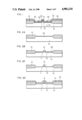
- FIG. 1 is a sectional view showing a structure of a MOSFET according to an embodiment of the present invention
- FIGS. 2A to 2H are sectional views for illustrating various steps for manufacturing the structure shown in FIG. 1;
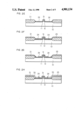
- FIGS. 3A and 3B show a portion of a MOSFET according to another embodiment of the invention in an equivalent circuit diagram and a sectional view, respectively;
- FIGS. 4A and 4B show a portion of a MOSFET according to still another embodiment of the invention in an equivalent circuit diagram and a sectional view;
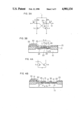
- FIGS. 5A to 5K are sectional views for illustrating various steps for manufacturing the structure shown in FIG. 4B.
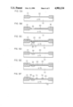
- FIG. 6 is a partial sectional view of a MOSFET device according to a further embodiment of the invention.
- FIG. 1 is a sectional view showing a portion of a semiconductor device according to an embodiment of the invention.
- a number of element regions i.e. regions for the elements constituting parts of the semiconductor device
- a silicon oxide film (field oxide) 21 of a relatively great thickness is formed on the surface of the p-type monocrystalline silicon substrate 10 except for the element regions, among which only one element region is shown in the drawing.
- the silicon oxide film 21 serves for isolation among the elements and is referred to as LOCOS (local oxidation of silicon) oxide film.
- a gate oxide film 20 on which a polycrystalline silicon layer 31 is formed to serve as a gate electrode.
- a source region 11 and a drain region 12 are Formed on the surface portions of the p-type monocrystalline silicon substrate 10 located on both sides of the gate electrode 31 .
- a source region 11 and a drain region 12 has a molybdenum (Mo) silicide layer 24 formed over the substantially whole region.
- Mo silicide layer 24 is formed over the substrate (inclusive of the surfaces of the polycrystalline silicon layer 31 and the silicon oxide film 21).
- polycrystalline silicon layers 33 which serve as interconnection layers brought into contact with the Mo silicide layers 24 through the contact holes.
- the molybdenum (Mo) silicide layer 24 is interposed between the silicon substrate 10 and the polycrystalline silicon layer 33 serving for the interconnection, as described above, contact of low resistance can be realized with an improved reproducibility. Further, because the diffused layer or doped region of the MOSFET is deposited thereon with the Mo silicide layer 24 over the whole surface thereof, lateral resistance of the diffused layer can be reduced, resulting in that the transconductance g m can be improved, to another advantage. It should be added that the deposition of the Mo silicide layer 24 over the gate electrode 31 allows resistance involved in the gate interconnection to be reduced, whereby contact to the polycrystalline silicon layer 31 serving as the gate electrode can be realized with low resistance.
- FIGS. 2A to 2H A method of manufacturing the semiconductor device described above will be elucidated by referring to FIGS. 2A to 2H.
- one major surface of the p-type monocrystalline silicon substrate 10 is first formed with a silicon oxide (Si0 2 ) thick film 21 serving for isolation of the elements through a selective oxidization (LOCOS) process, being followed by growth of a thin Si0 2 film 20 constituting the gate oxide film.
- LOC selective oxidization
- phosphorus (P) is thermally diffused into polycrystalline silicon for imparting electric conductivity.
- the polycrystalline silicon film is patterned through photo-etching technique to thereby form the gate electrode 31 of desired dimensions, as is shown in FIG. 2B.
- the regions which are to serve as the source and drain regions are implanted with arsenic (As) through ion beam irradiation process by employing the gate electrode 31 as the mask, to thereby form the self-aligned source and drain regions 11 and 12.
- the thin gate oxide film is partially removed through etching process known in the art to thereby expose the source region 11 and the drain region 12, as shown in FIG. 2C.
- a molybdenum (Mo) film 23 is deposited over the whole surface of the substrate in a thickness of 500 ⁇ through vacuum sputtering technique, as is shown in FIG. 2D. Then, the substrate undergoes heat treatment at 1000° C.
- the silicon oxide film 25 is deposited over the whole surface of the structure through CVD process (FIG. 2F).
- the contact holes or windows for the source region 11 and the drain region 12 are formed in the silicon oxide film 25 through photoetching technique (FIG. 2G).
- the polycrystalline silicon film 33 is deposited over the whole surface of the substrate through CVD process.
- the whole surface of the polycrystalline silicon film 33 is implanted with arsenic (As) through ion beam implantation, being followed by heat treatment at 1000° C. for ten minutes for imparting the electric conductivity.
- As arsenic
- FIG. 2H polycrystalline silicon is removed through photo-etching technique except for the polycrystalline silicon regions 33 serving for interconnection to the source region 11 and to the drain region 12. In this manner, the structure shown in FIG. 1 can be implemented.
- FIG. 3A is an equivalent circuit diagram of one memory cell and FIG. 3B is a sectional view showing a portion of the structure for realizing the circuit configuration shown in FIG. 3A.
- a pair of cross-wired MOSFETs Tr3 and Tr4 have respective load resistors R3 and R4 connected thereto. Junctions or interconnections A and B between the MOSFET Tr3 and the load resistor R3 and between the MOSFET Tr4 and the load resistor R4, respectively, are further connected to transfer gates Tr1 and Tr2, respectively, and additionally to the gates of the MOSFETs Tr4 and Tr3, respectively, of the counterpart branches, respectively. In this way, one cell of the static memory is implemented.
- FIG. 3B is a partial sectional view of the structure of a semiconductor device adapted for realizing the circuit shown in FIG. 3A and shows more specifically interconnection of the source/drain region 11 (junction B) of the MOSFET Tr2.
- the n + -type source/drain regions 11 and 12 are formed in a p-type silicon substrate 10 through ion implantation, diffusion or the like.
- the MOSFET Tr2 is circumferentially surrounded by a relatively thick field oxide film 21.
- Molybdenum silicide layers 24 are formed at the contact hole portions of the source and drain regions 11 and 12, respectively.
- a polycrystalline silicon interconnection layer 36 is connected to the Mo silicide layer 24 of the source/drain region 12 at the same level as the polycrystalline silicon layer 33.
- a Mo silicide layer is formed over the upper surface of the polycrystalline silicon layer 31 which serves as the gate electrode of the MOSFET Tr2.
- the structure shown in FIG. 3B differs from the one shown in FIG. 1 in that two polycrystalline silicon interconnection layers 30 and 33 are connected to the source/drain region 11 and that the molybdenum silicide layer is deposited only at the contact hole.
- connection of the polycrystalline silicon layers 30 and 33 to the Mo silicide layer 24 which in turn is connected to the source/drain region 11 with low contact resistance not only the contact resistance between the source/drain region 11 and the polycrystalline silicon layers 30 and 33 but also the connection resistance between the polycrystalline silicon layers 30 and 33 can be advantageously reduced.
- the interconnection layer 36 overlying the source/drain region 12 can be made of a metal instead of polycrystalline silicon.
- FIGS. 4A and 4B illustrate a structure in which two polycrystalline silicon interconnection layers are connected to one end of a serial connection of two MOSFETs Tr3 and Tr4. It should be noted that this structure may be realized as a part of the circuit shown in FIG. 3A.
- n + -type source/drain regions 11 and 12 are formed in a p-type silicon substrate 10 in a major surface thereof.
- the n + -type source/drain region 11 located to the leftmost includes a deep portion for connection and a shallow portion defining the source/drain of the MOSFET (the same applies also to the structure shown in FIG. 3B).
- contact resistance between the silicon substrate and the polycrystalline silicon layers 30 and 33 can be reduced because of interposition of the molybdenum silicide layer 24 between the former and the latter.
- the silicide layer 24 is so formed as to interconnect the polycrystalline silicon layers 30 and 33, connection resistance between these layers 30 and 33 can also be reduced, whereby characteristics of the implemented circuit can be improved.
- the reproducibility of contact between the silicon substrate and the polycrystalline silicon layers can be enhanced.
- the source/drain region 11 of the MOSFET is partially deposited with the silicide layer 24, lateral resistance of the region 11 can also be reduced.
- the transconductance g m of the MOSFET can also be improved.
- FIGS. 3A and 3B shares common features with the one shown in FIGS. 4A and 4B except for some differences.
- a method of manufacturing the structure shown in FIG. 4B will now be described by referring to FIGS. 5A to 5K. Modification of this method for realizing the structure shown in FIG. 3B will readily occur to those skilled in the art on the basis of the following description.
- a thick oxide (Si0 2 ) film 21 serving for isolation among the elements is first formed on a major surface of a p-type monocrystalline silicon substrate 10 through selective oxidization (LOCOS) process, being followed by formation of a thin Si0 2 -film 20.
- LOC selective oxidization
- a photoresist layer 16 is spun on the oxide film and a contact window 22 is formed through photolithography technique (FIG. 5B).
- the contact hole or window 22 is formed by removing a part of the oxide film 20 for forming a region to be doped to n + -type conductivity (FIG. 5B).
- a n + -type region 11' is formed through ion implantation of n-type impurity such as phosphorus (P) by using the photoresist layer as a mask or alternatively through diffusion by using the oxide film 20 as the mask. In the latter case, the oxide film is once removed, being followed by growth of a new oxide film 20 which is then formed with a window by using the same mask. Next, a molybdenum (Mo) film 23 of 500 ° ⁇ in thickness is deposited over the whole surface through vacuum sputtering method (FIG. 5C). The sub-structure thus obtained is subjected to heat treatment at 1000° C.
- n-type impurity such as phosphorus (P)
- molybdenum (Mo) silicide layer 24 selectively only at the window region 22.
- molybdenum undergoes no reaction with the Si02 films 20 and 21.
- molybdenum undergone no reaction is etched away by using aqua regia to leave the molybdenum (Mo) silicide layer on the contact hole region 22 (FIG. 5D).
- a polycrystalline silicon film 30 is deposited through CVD, which film 30 is then made electrically conductive through thermal diffusion of phosphorus (P) in the polycrystalline silicon film 30.
- a photoresist layer is then applied on the polycrystalline silicon film 30 for patterning the latter through photolithography and dry etching, to thereby form the gate electrodes 31 and 32 and interconnection 30 of desired dimensions (FIG. 5F).
- the gate electrode 31 is in the state electrically continuous to the interconnection layer 30.
- the whole surface is irradiated with an ion beam of arsenic (As) to thereby form n + -type source/drain regions 11 and 12, as shown in FIG. 5G.
- a CVD oxide (Si0 2 ) film 25 is deposited over the whole surface, as shown in FIG. 5H.
- the oxide film 25 is selectively etched away through photolithography, as is shown in FIG. 5I.
- a polycrystalline silicon film 33 is deposited through CVD, as shown in FIG. 5J, being followed by ion implantation of arsenic (As) and heat treatment.
- the polycrystalline silicon film 33 is then selectively etched away through photolithography and dry etching, while the portion of the film 33 overlying the polycrystalline silicon film 30 and the portion destined for interconnection to the layer 24 are left as they are (FIG. 5K). In this manner, the structure shown in FIG. 4B can be implemented.
- the molybdenum silicide layer serves as stopper for the dry etching, whereby the overetching of the silicon substrate at the region of the contact window can be effectively suppressed.
- nonuniformity in the characteristics of circuit elements due to the over-etched silicon substrate can be reduced, to an advantage.
- FIG. 6 shows a modification of the structure shown in FIG. 4B in which the polycrystalline silicon layer 33 is replaced by a metal layer 34. With the structure shown in FIG. 6, metal electrodes exhibiting contact resistance reduced more significantly can be realized.
- the metal for forming silicide there may be used other metals exhibiting a high melting point such as, for example, tungsten (W), titanium (Ti) and tantalum (Ta) in addition to molybdenum (Mo).
- W tungsten
- Ti titanium
- Ta tantalum
- Mo molybdenum
- the species of ions for use in ion implantation, the conditions of heat treatment and the order or sequence of processing steps may be changed.
- the polycrystalline silicon film serving as the gate may be replaced by a duplex structure consisting of a metal silicide and polycrystalline silicon.
- the polycrystalline silicon electrode and a portion of interconnections may be replaced by aluminium silicide electrode and interconnection to similar effect.
- deposition of the molybdenum film is realized by the vacuum sputtering.
- one selected from Mo, W, Ti, Ta and others may be deposited through CVD in the form of film on the silicon substrate at regions where no Si0 2 film is formed.
- a same metal layer as the one forming the overlying silicide layer may be formed over the latter to similar effect.
Abstract
A semiconductor LSI device formed in a semiconductor substrate comprising source/ drain regions of a MOSFET, polycrystalline silicon conductor to be connected to the source/drain region, and a silicide layer interposed between the source/drain region and the polycrystalline silicon conductor. Silicide intrudes into silicon bulk through an oxide film on the silicon substrate surface, assuring contact of low resistance, while lateral resistance of the source/drain region formed in the semiconductor substrate is also reduced. Reduction of contact/connection resistances is accomplished in a high density LSI which is thus imparted with an improved high-speed performance.
Description
This application is a continuation of application Ser. No. 794,687, filed Nov. 4, 1985now abandoned.
The present invention generally relates to a semiconductor device and a method of manufacturing the same. In particular, the invention concerns a semiconductor device incorporating polycrystalline silicon interconnections and a manufacturing method thereof.
In recent years, there arises an increasing tendency of using polycrystalline silicon in the semiconductor integrated circuit device for meeting the demand for implementation of high-speed semiconductor devices with high integration density. In particular, in the case of a MOSLSI in which insulated gate field effect transistors (IGFETs) are employed, there is obtained an advantage that the gate electrode of the IGFET and the interconnection layer can b formed of a same polycrystalline silicon layer. Besides, by selectively doping a polycrystalline silicon layer at regions with impurity at a high concentration to exhibit a low resistivity in such a manner that a polycrystalline silicon region of high resistivity is sandwiched therebetween, it is possible to incorporate resistors in the polycrystalline silicon layer. In other words, importance of polycrystalline silicon becomes predominant in the implementation of semiconductor devices and in particular in silicon IC device and silicon LSI device.
Polycrystalline silicon is usually formed through chemical vapor deposition (referred to as CVD in abbreviation), according to which silicon wafers are introduced into a heated quartz tube and supplied with a raw material gas (such as monosilane or the like), to thereby deposit polycrystalline silicon on the wafers. However, this method is accompanied with a problem that oxygen contained in the air may enter the quartz tube together with the wafers upon introducing wafers into the quartz tube, resulting in that exposed regions (contact holes or windows) of the silicon wafer will become oxidized more or less. As a consequence, a thin oxide film is formed between the silicon surface within the contact windows and the polycrystalline silicon film deposited on the silicon surface, whereby contact resistance of the polycrystalline silicon layer is increased, degrading the performance of the semiconductor device. In an extreme case, electric breakage (open-circuiting) will take place between the silicon wafer and the polycrystalline silicon layer, as the result of which yield of the manufactured semiconductor devices is decreased. Increasing the high integration density of the semiconductor LSI requires corresponding reduction of area available for a unit element, being accompanied with reduction in the area of the contact region (window). Under the circumstances, when the polycrystalline silicon layer is to be used for the interconnection in the manner known heretofore, the problem involved in the formation of the polycrystalline silicon layer as described above becomes more serious, providing the cause for the significant increase of the contact resistance as well as degradation of reproducibility (yield) of the contacts.
An object of the present invention is to provide a semiconductor device incorporating polycrystalline silicon interconnection layers of low contact resistance.
Another object of the invention is to provide a semiconductor device having polycrystalline silicon interconnection layers and an impurity-doped region exhibiting low lateral resistance.
As described hereinbefore, a thin oxide film formed on a silicon substrate upon deposition of a polycrystalline silicon layer on the substrate provides a main cause for increasing the contact resistance. It is observed that when a silicide layer is interposed between the polycrystalline silicon layer and the substrate, the silicide layer grows to intrude into the substrate through the oxide film, assuring thus an improved contact of low resistance. Besides, the doped region formed within the substrate having the silicide layer formed on the surface exhibits reduced lateral resistance. Accordingly, when the contact area of interconnection conductors is decreased for realizing LSI having an increased integration density, increase in contact resistance due to the reduced contact area can be suppressed to minimum.
FIG. 1 is a sectional view showing a structure of a MOSFET according to an embodiment of the present invention;
FIGS. 2A to 2H are sectional views for illustrating various steps for manufacturing the structure shown in FIG. 1;
FIGS. 3A and 3B show a portion of a MOSFET according to another embodiment of the invention in an equivalent circuit diagram and a sectional view, respectively;
FIGS. 4A and 4B show a portion of a MOSFET according to still another embodiment of the invention in an equivalent circuit diagram and a sectional view;
FIGS. 5A to 5K are sectional views for illustrating various steps for manufacturing the structure shown in FIG. 4B; and
FIG. 6 is a partial sectional view of a MOSFET device according to a further embodiment of the invention.
In the following, the invention will be described in detail in conjunction with the exemplary embodiments of the semiconductor device as well as the manufacturing method thereof by referring to the accompanying drawings.
FIG. 1 is a sectional view showing a portion of a semiconductor device according to an embodiment of the invention. As will be seen, a number of element regions (i.e. regions for the elements constituting parts of the semiconductor device) are formed on a major surface of a p-type monocrystalline silicon substrate 10. Additionally, a silicon oxide film (field oxide) 21 of a relatively great thickness is formed on the surface of the p-type monocrystalline silicon substrate 10 except for the element regions, among which only one element region is shown in the drawing. The silicon oxide film 21 serves for isolation among the elements and is referred to as LOCOS (local oxidation of silicon) oxide film. Formed at the center of the surface portion of the p-type monocrystalline silicon substrate 10 enclosed by the LOCOS oxide film 21 is a gate oxide film 20 on which a polycrystalline silicon layer 31 is formed to serve as a gate electrode. Formed on the surface portions of the p-type monocrystalline silicon substrate 10 located on both sides of the gate electrode 31 are a source region 11 and a drain region 12, respectively, through doping of n-type impurity. Each of the source region 11 and the drain region 12 has a molybdenum (Mo) silicide layer 24 formed over the substantially whole region. Except for portions (contact holes) of the Mo silicide layers 24, a CVD oxide film 25 is formed over the substrate (inclusive of the surfaces of the polycrystalline silicon layer 31 and the silicon oxide film 21). Finally, formed thereon are polycrystalline silicon layers 33 which serve as interconnection layers brought into contact with the Mo silicide layers 24 through the contact holes.
With the structure of the semiconductor device in which the molybdenum (Mo) silicide layer 24 is interposed between the silicon substrate 10 and the polycrystalline silicon layer 33 serving for the interconnection, as described above, contact of low resistance can be realized with an improved reproducibility. Further, because the diffused layer or doped region of the MOSFET is deposited thereon with the Mo silicide layer 24 over the whole surface thereof, lateral resistance of the diffused layer can be reduced, resulting in that the transconductance gm can be improved, to another advantage. It should be added that the deposition of the Mo silicide layer 24 over the gate electrode 31 allows resistance involved in the gate interconnection to be reduced, whereby contact to the polycrystalline silicon layer 31 serving as the gate electrode can be realized with low resistance.
A method of manufacturing the semiconductor device described above will be elucidated by referring to FIGS. 2A to 2H.
Referring to FIG. 2A, one major surface of the p-type monocrystalline silicon substrate 10 is first formed with a silicon oxide (Si02) thick film 21 serving for isolation of the elements through a selective oxidization (LOCOS) process, being followed by growth of a thin Si02 film 20 constituting the gate oxide film. Subsequently after the polycrystalline silicon film has been deposited over the whole surface through CVD process, phosphorus (P) is thermally diffused into polycrystalline silicon for imparting electric conductivity. Next, the polycrystalline silicon film is patterned through photo-etching technique to thereby form the gate electrode 31 of desired dimensions, as is shown in FIG. 2B. Subsequently, the regions which are to serve as the source and drain regions are implanted with arsenic (As) through ion beam irradiation process by employing the gate electrode 31 as the mask, to thereby form the self-aligned source and drain regions 11 and 12. Next, the thin gate oxide film is partially removed through etching process known in the art to thereby expose the source region 11 and the drain region 12, as shown in FIG. 2C. Subsequently, a molybdenum (Mo) film 23 is deposited over the whole surface of the substrate in a thickness of 500 Å through vacuum sputtering technique, as is shown in FIG. 2D. Then, the substrate undergoes heat treatment at 1000° C. for 30 minutes, thereby alloying the surfaces of silicon contacting directly the molybdenum film 23 (i.e. those of the source region 11, drain region 12 and the gate electrode 31), as the result of which the Mo silicide layers 24 are selectively formed. These M silicide layers are formed only on the silicon surfaces. The oxide film 21 undergoes no reaction with molybdenum. Accordingly, the molybdenum film on the oxide layer remains as it is. Subsequently, the molybdenum film 23 remaining on the oxide film 21 is etched away by using aqua regia, which results in the structure shown in FIG. 2E. It will be seen that Mo silicide films are left on the source region 11, the drain region 12 and the gate electrode 31. The silicon oxide film 25 is deposited over the whole surface of the structure through CVD process (FIG. 2F). The contact holes or windows for the source region 11 and the drain region 12 are formed in the silicon oxide film 25 through photoetching technique (FIG. 2G). Subsequently, the polycrystalline silicon film 33 is deposited over the whole surface of the substrate through CVD process. The whole surface of the polycrystalline silicon film 33 is implanted with arsenic (As) through ion beam implantation, being followed by heat treatment at 1000° C. for ten minutes for imparting the electric conductivity. Referring to FIG. 2H, polycrystalline silicon is removed through photo-etching technique except for the polycrystalline silicon regions 33 serving for interconnection to the source region 11 and to the drain region 12. In this manner, the structure shown in FIG. 1 can be implemented.
Next, description will be made on a MOS memory cell according to another embodiment of the present invention. FIG. 3A is an equivalent circuit diagram of one memory cell and FIG. 3B is a sectional view showing a portion of the structure for realizing the circuit configuration shown in FIG. 3A.
Referring to FIG. 3A, a pair of cross-wired MOSFETs Tr3 and Tr4 have respective load resistors R3 and R4 connected thereto. Junctions or interconnections A and B between the MOSFET Tr3 and the load resistor R3 and between the MOSFET Tr4 and the load resistor R4, respectively, are further connected to transfer gates Tr1 and Tr2, respectively, and additionally to the gates of the MOSFETs Tr4 and Tr3, respectively, of the counterpart branches, respectively. In this way, one cell of the static memory is implemented.
FIG. 3B is a partial sectional view of the structure of a semiconductor device adapted for realizing the circuit shown in FIG. 3A and shows more specifically interconnection of the source/drain region 11 (junction B) of the MOSFET Tr2. The n+ -type source/drain regions 11 and 12 are formed in a p-type silicon substrate 10 through ion implantation, diffusion or the like. The MOSFET Tr2 is circumferentially surrounded by a relatively thick field oxide film 21. Molybdenum silicide layers 24 are formed at the contact hole portions of the source and drain regions 11 and 12, respectively. Connected to the molybdenum silicide layer 24 of the source/drain region 11 are polycrystalline silicon layers 30 and 33 which are isolated from each other by a CVD oxide layer 25. On the other hand, a polycrystalline silicon interconnection layer 36 is connected to the Mo silicide layer 24 of the source/drain region 12 at the same level as the polycrystalline silicon layer 33. Further, a Mo silicide layer is formed over the upper surface of the polycrystalline silicon layer 31 which serves as the gate electrode of the MOSFET Tr2. The structure shown in FIG. 3B differs from the one shown in FIG. 1 in that two polycrystalline silicon interconnection layers 30 and 33 are connected to the source/drain region 11 and that the molybdenum silicide layer is deposited only at the contact hole.
By virtue of the connection of the polycrystalline silicon layers 30 and 33 to the Mo silicide layer 24 which in turn is connected to the source/drain region 11 with low contact resistance, not only the contact resistance between the source/drain region 11 and the polycrystalline silicon layers 30 and 33 but also the connection resistance between the polycrystalline silicon layers 30 and 33 can be advantageously reduced. It will be self-explanatory that the interconnection layer 36 overlying the source/drain region 12 can be made of a metal instead of polycrystalline silicon.
FIGS. 4A and 4B illustrate a structure in which two polycrystalline silicon interconnection layers are connected to one end of a serial connection of two MOSFETs Tr3 and Tr4. It should be noted that this structure may be realized as a part of the circuit shown in FIG. 3A.
Referring to the figures, n+ -type source/drain regions 11 and 12 are formed in a p-type silicon substrate 10 in a major surface thereof. The n+ -type source/drain region 11 located to the leftmost includes a deep portion for connection and a shallow portion defining the source/drain of the MOSFET (the same applies also to the structure shown in FIG. 3B).
According to the embodiment now under consideration, contact resistance between the silicon substrate and the polycrystalline silicon layers 30 and 33 can be reduced because of interposition of the molybdenum silicide layer 24 between the former and the latter. Besides, since the silicide layer 24 is so formed as to interconnect the polycrystalline silicon layers 30 and 33, connection resistance between these layers 30 and 33 can also be reduced, whereby characteristics of the implemented circuit can be improved. Further, the reproducibility of contact between the silicon substrate and the polycrystalline silicon layers can be enhanced. Additionally, since the source/drain region 11 of the MOSFET is partially deposited with the silicide layer 24, lateral resistance of the region 11 can also be reduced. Thus, the transconductance gm of the MOSFET can also be improved.
The structure shown in FIGS. 3A and 3B shares common features with the one shown in FIGS. 4A and 4B except for some differences. A method of manufacturing the structure shown in FIG. 4B will now be described by referring to FIGS. 5A to 5K. Modification of this method for realizing the structure shown in FIG. 3B will readily occur to those skilled in the art on the basis of the following description.
Referring to FIG. 5A, a thick oxide (Si02) film 21 serving for isolation among the elements is first formed on a major surface of a p-type monocrystalline silicon substrate 10 through selective oxidization (LOCOS) process, being followed by formation of a thin Si02 -film 20. A photoresist layer 16 is spun on the oxide film and a contact window 22 is formed through photolithography technique (FIG. 5B). The contact hole or window 22 is formed by removing a part of the oxide film 20 for forming a region to be doped to n+ -type conductivity (FIG. 5B). A n+ -type region 11' is formed through ion implantation of n-type impurity such as phosphorus (P) by using the photoresist layer as a mask or alternatively through diffusion by using the oxide film 20 as the mask. In the latter case, the oxide film is once removed, being followed by growth of a new oxide film 20 which is then formed with a window by using the same mask. Next, a molybdenum (Mo) film 23 of 500 ° Å in thickness is deposited over the whole surface through vacuum sputtering method (FIG. 5C). The sub-structure thus obtained is subjected to heat treatment at 1000° C. for 30 minutes to thereby cause silicon (at the surface of the window region 22) which is in direct contact with the molybdenum film 23 to react with molybdenum, to thereby form a molybdenum (Mo) silicide layer 24 selectively only at the window region 22. It is noted that molybdenum undergoes no reaction with the Si02 films 20 and 21. Subsequently, molybdenum undergone no reaction is etched away by using aqua regia to leave the molybdenum (Mo) silicide layer on the contact hole region 22 (FIG. 5D). Next, a polycrystalline silicon film 30 is deposited through CVD, which film 30 is then made electrically conductive through thermal diffusion of phosphorus (P) in the polycrystalline silicon film 30. A photoresist layer is then applied on the polycrystalline silicon film 30 for patterning the latter through photolithography and dry etching, to thereby form the gate electrodes 31 and 32 and interconnection 30 of desired dimensions (FIG. 5F). It should be noted that the gate electrode 31 is in the state electrically continuous to the interconnection layer 30. Subsequently, the whole surface is irradiated with an ion beam of arsenic (As) to thereby form n+ -type source/drain regions 11 and 12, as shown in FIG. 5G. Next, a CVD oxide (Si02) film 25 is deposited over the whole surface, as shown in FIG. 5H. Subsequently, the oxide film 25 is selectively etched away through photolithography, as is shown in FIG. 5I. Then, a polycrystalline silicon film 33 is deposited through CVD, as shown in FIG. 5J, being followed by ion implantation of arsenic (As) and heat treatment. The polycrystalline silicon film 33 is then selectively etched away through photolithography and dry etching, while the portion of the film 33 overlying the polycrystalline silicon film 30 and the portion destined for interconnection to the layer 24 are left as they are (FIG. 5K). In this manner, the structure shown in FIG. 4B can be implemented.
It should be mentioned here that the molybdenum silicide layer serves as stopper for the dry etching, whereby the overetching of the silicon substrate at the region of the contact window can be effectively suppressed. Thus, nonuniformity in the characteristics of circuit elements due to the over-etched silicon substrate can be reduced, to an advantage.
FIG. 6 shows a modification of the structure shown in FIG. 4B in which the polycrystalline silicon layer 33 is replaced by a metal layer 34. With the structure shown in FIG. 6, metal electrodes exhibiting contact resistance reduced more significantly can be realized.
In the foregoing, the invention has been described in conjunction with exemplary embodiments thereof. It will however be appreciated that numerous modifications may be made without departing from the spirit and scope of the invention. As the metal for forming silicide, there may be used other metals exhibiting a high melting point such as, for example, tungsten (W), titanium (Ti) and tantalum (Ta) in addition to molybdenum (Mo). With regards to the manufacturing process, the species of ions for use in ion implantation, the conditions of heat treatment and the order or sequence of processing steps may be changed. Further, the polycrystalline silicon film serving as the gate may be replaced by a duplex structure consisting of a metal silicide and polycrystalline silicon. The polycrystalline silicon electrode and a portion of interconnections may be replaced by aluminium silicide electrode and interconnection to similar effect. In the case of the embodiments described hereinbefore, deposition of the molybdenum film is realized by the vacuum sputtering. However, one selected from Mo, W, Ti, Ta and others may be deposited through CVD in the form of film on the silicon substrate at regions where no Si02 film is formed. Further, a same metal layer as the one forming the overlying silicide layer may be formed over the latter to similar effect.
Claims (23)
1. A semiconductor device comprising:
a semiconductor substrate having a region doped with impurity of an conductivity type differing from that of said semiconductor substrate, the impurity-doped region including a relatively deep portion intruding into the semiconductor substrate and a relatively shallow portion;
an insulation layer having a window through which at least part of said relatively deep portion of said impurity-doped region is exposed;
a silicide layer formed on said relatively deep portion of said impurity-doped region, the relatively deep portion and the silicide layer being substantially aligned with said window; and
at least two electrodes each directly contacting said silicide layer, one of said electrodes being mainly formed of a same main component material as said semiconductor substrate.
2. A semiconductor device according to claim 1, wherein said semiconductor device includes an insulated gate field effect transistor (IGFET), said impurity-doped region constituting one of source/drain regions of said IGFET.
3. A semiconductor device according to claim 1, wherein said semiconductor device includes at least two IGFETs, and said one electrode is connected to a source/drain region of one of said IGFETs and serves as a gate electrode of the other IGFET.
4. A semiconductor device according to claim 1, wherein said semiconductor substrate is silicon, and said one of said at least two electrodes is formed of polycrystalline silicon.
5. A semiconductor device according to claim 1, wherein said silicide layer extends over substantially the whole surface of said impurity-doped region.
6. A semiconductor device according to claim 4, wherein said polycrystalline electrodes extend over only part of said silicide layer.
7. A semiconductor device according to claim 1, wherein said window exposes only a portion of said impurity-doped region.
8. A semiconductor device according to claim 1, wherein at least one of said at least two electrodes is formed of metal, and at least one of said at least two electrodes is formed of polycrystalline silicon.
9. A semiconductor device according to claim 1, wherein said silicide is selected from the group consisting of molybdenum, tungsten, titanium and tantalum.
10. A semiconductor device according to claim 7, wherein said silicide layer extends only in the area substantially equal to the area exposed in said window.
11. A semiconductor device comprising:
a semiconductor substrate having a region doped with impurity of a conductivity type differing from that of said semiconductor substrate, the impurity-doped region including a relatively deep portion intruding into the semiconductor substrate and a relatively shallow portion;
an insulation layer having a window through which at least part of said relatively deep portion of said impurity-doped region is exposed;
a silicide layer formed on said relatively deep portion of said impurity-doped region, said relatively deep portion and said silicide layer having substantially a same shape, in plan view, as said window; and
at least two electrodes each directly contacting said silicide layer, one of said electrodes being mainly formed of a same main component material as said semiconductor substrate, said electrodes having a low connection resistance in the interconnection therebetween and a low contact resistance in the contact between each of the electrodes and the impurity-doped region, as compared to the connection and contact resistances without a silicide layer between the at least two electrodes and the impurity-doped region.
12. A semiconductor device according to claim 11, wherein said semiconductor device includes an insulated gate field effect transistor (IGFET), said impurity-doped region constituting one of source/drain regions of said IGFET.
13. A semiconductor device according to claim 11, wherein said semiconductor device includes at least two IGFETs, and said one electrode is connected to a source/drain region of one of said IGFETs and serves as a gate electrode of the other IGFET.
14. A semiconductor device according to claim 11, wherein said semiconductor substrate is silicon and said one of at least two electrodes is formed of polycrystalline silicon.
15. A semiconductor device according to claim 11, wherein said silicide layer extends over substantially the whole surface of said impurity-doped region.
16. A semiconductor device according to claim 14, wherein said polycrystalline electrodes extends over only part of said silicide layer.
17. A semiconductor device according to claim 11, wherein said window exposes only a portion of said impurity-doped region.
18. A semiconductor device according to claim 11, wherein at least one of said at least two electrodes is formed of metal, and at least one of said at least electrodes is formed of polycrystalline silicon.
19. A semiconductor device according to claim 11, wherein said silicide is selected from the group consisting of molybdenum, tungsten, titanium and tantalum.
20. A semiconductor device according to claim 17, wherein said silicide layer extends only in the area substantially equal to the area exposed in said window.
21. A semiconductor device according to claim 1, wherein each of the at least two electrodes directly contact the silicide only over the relatively deep portion of the impurity-doped region.
22. A semiconductor device according to claim 1, wherein the semiconductor device is a field effect transistor, the relatively shallow portion being a source or drain region of the field effect transistor, and the relatively deep portion being a portion for connection of the at least two electrodes to the source or drain region.
23. A semiconductor device according to claim 1, wherein the relatively deep portion is a portion for connection of the at least two electrodes to the impurity-doped region.
Applications Claiming Priority (4)
| Application Number | Priority Date | Filing Date | Title |
|---|---|---|---|
| JP23148984A JPS61110462A (en) | 1984-11-02 | 1984-11-02 | Semiconductor device and manufacture thereof |
| JP59-231489 | 1984-11-02 | ||
| JP59251376A JPH0682681B2 (en) | 1984-11-28 | 1984-11-28 | Semiconductor device and manufacturing method thereof |
| JP59-251376 | 1984-11-28 |
Related Parent Applications (1)
| Application Number | Title | Priority Date | Filing Date |
|---|---|---|---|
| US06794687 Continuation | 1985-11-04 |
Publications (1)
| Publication Number | Publication Date |
|---|---|
| US4901134A true US4901134A (en) | 1990-02-13 |
Family
ID=26529904
Family Applications (1)
| Application Number | Title | Priority Date | Filing Date |
|---|---|---|---|
| US07/184,370 Expired - Fee Related US4901134A (en) | 1984-11-02 | 1988-04-21 | Semiconductor device and manufacturing method thereof |
Country Status (3)
| Country | Link |
|---|---|
| US (1) | US4901134A (en) |
| EP (1) | EP0183995B1 (en) |
| DE (1) | DE3572423D1 (en) |
Cited By (14)
| Publication number | Priority date | Publication date | Assignee | Title |
|---|---|---|---|---|
| US4985740A (en) * | 1989-06-01 | 1991-01-15 | General Electric Company | Power field effect devices having low gate sheet resistance and low ohmic contact resistance |
| US5063422A (en) * | 1988-06-20 | 1991-11-05 | At&T Bell Laboratories | Devices having shallow junctions |
| US5079617A (en) * | 1988-09-20 | 1992-01-07 | Mitsubishi Denki Kabushiki Kaisha | Multiple layer electrode structure for semiconductor device and method of manufacturing thereof |
| US5146309A (en) * | 1989-06-23 | 1992-09-08 | Sgs-Thomson Microelectronics, Inc. | Method for forming polycrystalline silicon contacts |
| US5175118A (en) * | 1988-09-20 | 1992-12-29 | Mitsubishi Denki Kabushiki Kaisha | Multiple layer electrode structure for semiconductor device and method of manufacturing thereof |
| US5200637A (en) * | 1988-12-15 | 1993-04-06 | Kabushiki Kaisha Toshiba | MOS transistor and differential amplifier circuit with low offset |
| US5272099A (en) * | 1992-11-27 | 1993-12-21 | Etron Technology Inc. | Fabrication of transistor contacts |
| US5283449A (en) * | 1990-08-09 | 1994-02-01 | Nec Corporation | Semiconductor integrated circuit device including two types of MOSFETS having source/drain region different in sheet resistance from each other |
| US5336911A (en) * | 1988-05-10 | 1994-08-09 | Seiko Epson Corporation | Semiconductor device |
| US5410174A (en) * | 1991-07-31 | 1995-04-25 | Sgs-Thomson Microelectronics, Inc. | Contact structure for integrated circuits |
| US5589418A (en) * | 1993-08-04 | 1996-12-31 | Sgs-Thomson Microelectronics, Inc. | Method of forming a polysilicon buried contact |
| US6136698A (en) * | 1999-06-04 | 2000-10-24 | United Integrated Circuits Corp | Method of increasing contact area of a contact window |
| US6346465B1 (en) | 1997-06-23 | 2002-02-12 | Nec Corportion | Semiconductor device with silicide contact structure and fabrication method thereof |
| US20050102014A1 (en) * | 2003-11-07 | 2005-05-12 | Lilip Lau | Cardiac harness for treating congestive heart failure and for defibrillating and/or pacing/sensing |
Families Citing this family (3)
| Publication number | Priority date | Publication date | Assignee | Title |
|---|---|---|---|---|
| DE3724612A1 (en) * | 1987-07-24 | 1989-02-02 | Siemens Ag | Method for producing a semiconductor component |
| GB2222416B (en) * | 1988-08-31 | 1993-03-03 | Watkins Johnson Co | Processes using disilane |
| JP2727818B2 (en) * | 1991-09-17 | 1998-03-18 | 日本電気株式会社 | Semiconductor device |
Citations (4)
| Publication number | Priority date | Publication date | Assignee | Title |
|---|---|---|---|---|
| GB2082387A (en) * | 1980-08-15 | 1982-03-03 | Hitachi Ltd | A semiconductor device and a process for producing the same |
| US4453175A (en) * | 1979-09-19 | 1984-06-05 | Tokyo Shibaura Denki Kabushiki Kaisha | MOS Static RAM layout with polysilicon resistors over FET gates |
| US4558507A (en) * | 1982-11-12 | 1985-12-17 | Nec Corporation | Method of manufacturing semiconductor device |
| US4622735A (en) * | 1980-12-12 | 1986-11-18 | Tokyo Shibaura Denki Kabushiki Kaisha | Method for manufacturing a semiconductor device utilizing self-aligned silicide regions |
Family Cites Families (1)
| Publication number | Priority date | Publication date | Assignee | Title |
|---|---|---|---|---|
| JPS6164166A (en) * | 1984-09-06 | 1986-04-02 | Toshiba Corp | Semiconductor device |
-
1985
- 1985-10-31 DE DE8585113904T patent/DE3572423D1/en not_active Expired
- 1985-10-31 EP EP85113904A patent/EP0183995B1/en not_active Expired
-
1988
- 1988-04-21 US US07/184,370 patent/US4901134A/en not_active Expired - Fee Related
Patent Citations (4)
| Publication number | Priority date | Publication date | Assignee | Title |
|---|---|---|---|---|
| US4453175A (en) * | 1979-09-19 | 1984-06-05 | Tokyo Shibaura Denki Kabushiki Kaisha | MOS Static RAM layout with polysilicon resistors over FET gates |
| GB2082387A (en) * | 1980-08-15 | 1982-03-03 | Hitachi Ltd | A semiconductor device and a process for producing the same |
| US4622735A (en) * | 1980-12-12 | 1986-11-18 | Tokyo Shibaura Denki Kabushiki Kaisha | Method for manufacturing a semiconductor device utilizing self-aligned silicide regions |
| US4558507A (en) * | 1982-11-12 | 1985-12-17 | Nec Corporation | Method of manufacturing semiconductor device |
Non-Patent Citations (2)
| Title |
|---|
| Okabayashi et al., "Low-Resistance MOS Technology Using Self-Aligned Refractory Silicidation", IEEE Transactions on Electron Devices, ED-31, No. 9, Sep. 84, pp. 1329-1333. |
| Okabayashi et al., Low Resistance MOS Technology Using Self Aligned Refractory Silicidation , IEEE Transactions on Electron Devices, ED 31, No. 9, Sep. 84, pp. 1329 1333. * |
Cited By (14)
| Publication number | Priority date | Publication date | Assignee | Title |
|---|---|---|---|---|
| US5336911A (en) * | 1988-05-10 | 1994-08-09 | Seiko Epson Corporation | Semiconductor device |
| US5063422A (en) * | 1988-06-20 | 1991-11-05 | At&T Bell Laboratories | Devices having shallow junctions |
| US5079617A (en) * | 1988-09-20 | 1992-01-07 | Mitsubishi Denki Kabushiki Kaisha | Multiple layer electrode structure for semiconductor device and method of manufacturing thereof |
| US5175118A (en) * | 1988-09-20 | 1992-12-29 | Mitsubishi Denki Kabushiki Kaisha | Multiple layer electrode structure for semiconductor device and method of manufacturing thereof |
| US5200637A (en) * | 1988-12-15 | 1993-04-06 | Kabushiki Kaisha Toshiba | MOS transistor and differential amplifier circuit with low offset |
| US4985740A (en) * | 1989-06-01 | 1991-01-15 | General Electric Company | Power field effect devices having low gate sheet resistance and low ohmic contact resistance |
| US5146309A (en) * | 1989-06-23 | 1992-09-08 | Sgs-Thomson Microelectronics, Inc. | Method for forming polycrystalline silicon contacts |
| US5283449A (en) * | 1990-08-09 | 1994-02-01 | Nec Corporation | Semiconductor integrated circuit device including two types of MOSFETS having source/drain region different in sheet resistance from each other |
| US5410174A (en) * | 1991-07-31 | 1995-04-25 | Sgs-Thomson Microelectronics, Inc. | Contact structure for integrated circuits |
| US5272099A (en) * | 1992-11-27 | 1993-12-21 | Etron Technology Inc. | Fabrication of transistor contacts |
| US5589418A (en) * | 1993-08-04 | 1996-12-31 | Sgs-Thomson Microelectronics, Inc. | Method of forming a polysilicon buried contact |
| US6346465B1 (en) | 1997-06-23 | 2002-02-12 | Nec Corportion | Semiconductor device with silicide contact structure and fabrication method thereof |
| US6136698A (en) * | 1999-06-04 | 2000-10-24 | United Integrated Circuits Corp | Method of increasing contact area of a contact window |
| US20050102014A1 (en) * | 2003-11-07 | 2005-05-12 | Lilip Lau | Cardiac harness for treating congestive heart failure and for defibrillating and/or pacing/sensing |
Also Published As
| Publication number | Publication date |
|---|---|
| EP0183995B1 (en) | 1989-08-16 |
| DE3572423D1 (en) | 1989-09-21 |
| EP0183995A1 (en) | 1986-06-11 |
Similar Documents
| Publication | Publication Date | Title |
|---|---|---|
| US4901134A (en) | Semiconductor device and manufacturing method thereof | |
| US4392150A (en) | MOS Integrated circuit having refractory metal or metal silicide interconnect layer | |
| US5268590A (en) | CMOS device and process | |
| US4425700A (en) | Semiconductor device and method for manufacturing the same | |
| US4533935A (en) | Semiconductor device and a method for manufacturing the same | |
| US5512502A (en) | Manufacturing method for semiconductor integrated circuit device | |
| EP0052450A1 (en) | Method of manufacturing a semiconductor device with polycrystalline semiconductor cum metal electrodes | |
| US4663825A (en) | Method of manufacturing semiconductor device | |
| JPH0343778B2 (en) | ||
| US5851869A (en) | Manufacture of semiconductor device having low contact resistance | |
| JPH0644603B2 (en) | Semiconductor device and its manufacturing method | |
| US4693925A (en) | Integrated circuit structure having intermediate metal silicide layer | |
| US4985746A (en) | Semiconductor device and method of production | |
| JP3626773B2 (en) | Conductive layer of semiconductor device, MOSFET, and manufacturing method thereof | |
| GB2077993A (en) | Low sheet resistivity composite conductor gate MOS device | |
| US5652183A (en) | Method for fabricating semiconductor device containing excessive silicon in metal silicide film | |
| KR950001950B1 (en) | Method of making mos fet within ic | |
| US4924281A (en) | Gate structure for a MOS FET | |
| US5612557A (en) | Semiconductor device having an inter-layer insulating film disposed between two wiring layers | |
| US5521416A (en) | Semiconductor device having gate electrode and impurity diffusion layer different in conductivity type and method of manufacturing the same | |
| US5138425A (en) | Semiconductor integrated circuit device with nitride barrier layer ion implanted with resistivity decreasing elements | |
| JP3794915B2 (en) | Manufacturing method of semiconductor device | |
| US5714411A (en) | Process for forming a semiconductor device including a capacitor | |
| JPH065696B2 (en) | Method for manufacturing semiconductor device | |
| US6521517B1 (en) | Method of fabricating a gate electrode using a second conductive layer as a mask in the formation of an insulating layer by oxidation of a first conductive layer |
Legal Events
| Date | Code | Title | Description |
|---|---|---|---|
| FEPP | Fee payment procedure |
Free format text: PAYOR NUMBER ASSIGNED (ORIGINAL EVENT CODE: ASPN); ENTITY STATUS OF PATENT OWNER: LARGE ENTITY |
|
| FPAY | Fee payment |
Year of fee payment: 4 |
|
| REMI | Maintenance fee reminder mailed | ||
| LAPS | Lapse for failure to pay maintenance fees | ||
| FP | Lapsed due to failure to pay maintenance fee |
Effective date: 19980218 |
|
| STCH | Information on status: patent discontinuation |
Free format text: PATENT EXPIRED DUE TO NONPAYMENT OF MAINTENANCE FEES UNDER 37 CFR 1.362 |