US4912844A - Methods of producing printed circuit boards - Google Patents
Methods of producing printed circuit boards Download PDFInfo
- Publication number
- US4912844A US4912844A US07/230,460 US23046088A US4912844A US 4912844 A US4912844 A US 4912844A US 23046088 A US23046088 A US 23046088A US 4912844 A US4912844 A US 4912844A
- Authority
- US
- United States
- Prior art keywords
- substrate
- grooves
- punch
- cavities
- planar surface
- Prior art date
- Legal status (The legal status is an assumption and is not a legal conclusion. Google has not performed a legal analysis and makes no representation as to the accuracy of the status listed.)
- Expired - Lifetime
Links
Images


Classifications
-
- H—ELECTRICITY
- H05—ELECTRIC TECHNIQUES NOT OTHERWISE PROVIDED FOR
- H05K—PRINTED CIRCUITS; CASINGS OR CONSTRUCTIONAL DETAILS OF ELECTRIC APPARATUS; MANUFACTURE OF ASSEMBLAGES OF ELECTRICAL COMPONENTS
- H05K3/00—Apparatus or processes for manufacturing printed circuits
- H05K3/10—Apparatus or processes for manufacturing printed circuits in which conductive material is applied to the insulating support in such a manner as to form the desired conductive pattern
- H05K3/107—Apparatus or processes for manufacturing printed circuits in which conductive material is applied to the insulating support in such a manner as to form the desired conductive pattern by filling grooves in the support with conductive material
-
- H—ELECTRICITY
- H05—ELECTRIC TECHNIQUES NOT OTHERWISE PROVIDED FOR
- H05K—PRINTED CIRCUITS; CASINGS OR CONSTRUCTIONAL DETAILS OF ELECTRIC APPARATUS; MANUFACTURE OF ASSEMBLAGES OF ELECTRICAL COMPONENTS
- H05K3/00—Apparatus or processes for manufacturing printed circuits
- H05K3/0011—Working of insulating substrates or insulating layers
- H05K3/0014—Shaping of the substrate, e.g. by moulding
-
- H—ELECTRICITY
- H05—ELECTRIC TECHNIQUES NOT OTHERWISE PROVIDED FOR
- H05K—PRINTED CIRCUITS; CASINGS OR CONSTRUCTIONAL DETAILS OF ELECTRIC APPARATUS; MANUFACTURE OF ASSEMBLAGES OF ELECTRICAL COMPONENTS
- H05K3/00—Apparatus or processes for manufacturing printed circuits
- H05K3/02—Apparatus or processes for manufacturing printed circuits in which the conductive material is applied to the surface of the insulating support and is thereafter removed from such areas of the surface which are not intended for current conducting or shielding
- H05K3/04—Apparatus or processes for manufacturing printed circuits in which the conductive material is applied to the surface of the insulating support and is thereafter removed from such areas of the surface which are not intended for current conducting or shielding the conductive material being removed mechanically, e.g. by punching
- H05K3/041—Apparatus or processes for manufacturing printed circuits in which the conductive material is applied to the surface of the insulating support and is thereafter removed from such areas of the surface which are not intended for current conducting or shielding the conductive material being removed mechanically, e.g. by punching by using a die for cutting the conductive material
-
- H—ELECTRICITY
- H05—ELECTRIC TECHNIQUES NOT OTHERWISE PROVIDED FOR
- H05K—PRINTED CIRCUITS; CASINGS OR CONSTRUCTIONAL DETAILS OF ELECTRIC APPARATUS; MANUFACTURE OF ASSEMBLAGES OF ELECTRICAL COMPONENTS
- H05K3/00—Apparatus or processes for manufacturing printed circuits
- H05K3/02—Apparatus or processes for manufacturing printed circuits in which the conductive material is applied to the surface of the insulating support and is thereafter removed from such areas of the surface which are not intended for current conducting or shielding
- H05K3/04—Apparatus or processes for manufacturing printed circuits in which the conductive material is applied to the surface of the insulating support and is thereafter removed from such areas of the surface which are not intended for current conducting or shielding the conductive material being removed mechanically, e.g. by punching
- H05K3/045—Apparatus or processes for manufacturing printed circuits in which the conductive material is applied to the surface of the insulating support and is thereafter removed from such areas of the surface which are not intended for current conducting or shielding the conductive material being removed mechanically, e.g. by punching by making a conductive layer having a relief pattern, followed by abrading of the raised portions
-
- H—ELECTRICITY
- H05—ELECTRIC TECHNIQUES NOT OTHERWISE PROVIDED FOR
- H05K—PRINTED CIRCUITS; CASINGS OR CONSTRUCTIONAL DETAILS OF ELECTRIC APPARATUS; MANUFACTURE OF ASSEMBLAGES OF ELECTRICAL COMPONENTS
- H05K3/00—Apparatus or processes for manufacturing printed circuits
- H05K3/30—Assembling printed circuits with electric components, e.g. with resistor
- H05K3/32—Assembling printed circuits with electric components, e.g. with resistor electrically connecting electric components or wires to printed circuits
- H05K3/34—Assembling printed circuits with electric components, e.g. with resistor electrically connecting electric components or wires to printed circuits by soldering
- H05K3/3457—Solder materials or compositions; Methods of application thereof
-
- H—ELECTRICITY
- H05—ELECTRIC TECHNIQUES NOT OTHERWISE PROVIDED FOR
- H05K—PRINTED CIRCUITS; CASINGS OR CONSTRUCTIONAL DETAILS OF ELECTRIC APPARATUS; MANUFACTURE OF ASSEMBLAGES OF ELECTRICAL COMPONENTS
- H05K1/00—Printed circuits
- H05K1/02—Details
- H05K1/0201—Thermal arrangements, e.g. for cooling, heating or preventing overheating
- H05K1/0203—Cooling of mounted components
- H05K1/021—Components thermally connected to metal substrates or heat-sinks by insert mounting
-
- H—ELECTRICITY
- H05—ELECTRIC TECHNIQUES NOT OTHERWISE PROVIDED FOR
- H05K—PRINTED CIRCUITS; CASINGS OR CONSTRUCTIONAL DETAILS OF ELECTRIC APPARATUS; MANUFACTURE OF ASSEMBLAGES OF ELECTRICAL COMPONENTS
- H05K1/00—Printed circuits
- H05K1/02—Details
- H05K1/03—Use of materials for the substrate
- H05K1/05—Insulated conductive substrates, e.g. insulated metal substrate
- H05K1/056—Insulated conductive substrates, e.g. insulated metal substrate the metal substrate being covered by an organic insulating layer
-
- H—ELECTRICITY
- H05—ELECTRIC TECHNIQUES NOT OTHERWISE PROVIDED FOR
- H05K—PRINTED CIRCUITS; CASINGS OR CONSTRUCTIONAL DETAILS OF ELECTRIC APPARATUS; MANUFACTURE OF ASSEMBLAGES OF ELECTRICAL COMPONENTS
- H05K1/00—Printed circuits
- H05K1/02—Details
- H05K1/09—Use of materials for the conductive, e.g. metallic pattern
-
- H—ELECTRICITY
- H05—ELECTRIC TECHNIQUES NOT OTHERWISE PROVIDED FOR
- H05K—PRINTED CIRCUITS; CASINGS OR CONSTRUCTIONAL DETAILS OF ELECTRIC APPARATUS; MANUFACTURE OF ASSEMBLAGES OF ELECTRICAL COMPONENTS
- H05K1/00—Printed circuits
- H05K1/18—Printed circuits structurally associated with non-printed electric components
- H05K1/182—Printed circuits structurally associated with non-printed electric components associated with components mounted in the printed circuit board, e.g. insert mounted components [IMC]
- H05K1/183—Components mounted in and supported by recessed areas of the printed circuit board
-
- H—ELECTRICITY
- H05—ELECTRIC TECHNIQUES NOT OTHERWISE PROVIDED FOR
- H05K—PRINTED CIRCUITS; CASINGS OR CONSTRUCTIONAL DETAILS OF ELECTRIC APPARATUS; MANUFACTURE OF ASSEMBLAGES OF ELECTRICAL COMPONENTS
- H05K2201/00—Indexing scheme relating to printed circuits covered by H05K1/00
- H05K2201/01—Dielectrics
- H05K2201/0104—Properties and characteristics in general
- H05K2201/0129—Thermoplastic polymer, e.g. auto-adhesive layer; Shaping of thermoplastic polymer
-
- H—ELECTRICITY
- H05—ELECTRIC TECHNIQUES NOT OTHERWISE PROVIDED FOR
- H05K—PRINTED CIRCUITS; CASINGS OR CONSTRUCTIONAL DETAILS OF ELECTRIC APPARATUS; MANUFACTURE OF ASSEMBLAGES OF ELECTRICAL COMPONENTS
- H05K2201/00—Indexing scheme relating to printed circuits covered by H05K1/00
- H05K2201/03—Conductive materials
- H05K2201/0302—Properties and characteristics in general
- H05K2201/0305—Solder used for other purposes than connections between PCB or components, e.g. for filling vias or for programmable patterns
-
- H—ELECTRICITY
- H05—ELECTRIC TECHNIQUES NOT OTHERWISE PROVIDED FOR
- H05K—PRINTED CIRCUITS; CASINGS OR CONSTRUCTIONAL DETAILS OF ELECTRIC APPARATUS; MANUFACTURE OF ASSEMBLAGES OF ELECTRICAL COMPONENTS
- H05K2201/00—Indexing scheme relating to printed circuits covered by H05K1/00
- H05K2201/03—Conductive materials
- H05K2201/0332—Structure of the conductor
- H05K2201/0335—Layered conductors or foils
- H05K2201/0355—Metal foils
-
- H—ELECTRICITY
- H05—ELECTRIC TECHNIQUES NOT OTHERWISE PROVIDED FOR
- H05K—PRINTED CIRCUITS; CASINGS OR CONSTRUCTIONAL DETAILS OF ELECTRIC APPARATUS; MANUFACTURE OF ASSEMBLAGES OF ELECTRICAL COMPONENTS
- H05K2201/00—Indexing scheme relating to printed circuits covered by H05K1/00
- H05K2201/03—Conductive materials
- H05K2201/0332—Structure of the conductor
- H05K2201/0364—Conductor shape
- H05K2201/0376—Flush conductors, i.e. flush with the surface of the printed circuit
-
- H—ELECTRICITY
- H05—ELECTRIC TECHNIQUES NOT OTHERWISE PROVIDED FOR
- H05K—PRINTED CIRCUITS; CASINGS OR CONSTRUCTIONAL DETAILS OF ELECTRIC APPARATUS; MANUFACTURE OF ASSEMBLAGES OF ELECTRICAL COMPONENTS
- H05K2201/00—Indexing scheme relating to printed circuits covered by H05K1/00
- H05K2201/03—Conductive materials
- H05K2201/0332—Structure of the conductor
- H05K2201/0364—Conductor shape
- H05K2201/0382—Continuously deformed conductors
-
- H—ELECTRICITY
- H05—ELECTRIC TECHNIQUES NOT OTHERWISE PROVIDED FOR
- H05K—PRINTED CIRCUITS; CASINGS OR CONSTRUCTIONAL DETAILS OF ELECTRIC APPARATUS; MANUFACTURE OF ASSEMBLAGES OF ELECTRICAL COMPONENTS
- H05K2201/00—Indexing scheme relating to printed circuits covered by H05K1/00
- H05K2201/09—Shape and layout
- H05K2201/09009—Substrate related
- H05K2201/09036—Recesses or grooves in insulating substrate
-
- H—ELECTRICITY
- H05—ELECTRIC TECHNIQUES NOT OTHERWISE PROVIDED FOR
- H05K—PRINTED CIRCUITS; CASINGS OR CONSTRUCTIONAL DETAILS OF ELECTRIC APPARATUS; MANUFACTURE OF ASSEMBLAGES OF ELECTRICAL COMPONENTS
- H05K2203/00—Indexing scheme relating to apparatus or processes for manufacturing printed circuits covered by H05K3/00
- H05K2203/01—Tools for processing; Objects used during processing
- H05K2203/0104—Tools for processing; Objects used during processing for patterning or coating
- H05K2203/0108—Male die used for patterning, punching or transferring
-
- H—ELECTRICITY
- H05—ELECTRIC TECHNIQUES NOT OTHERWISE PROVIDED FOR
- H05K—PRINTED CIRCUITS; CASINGS OR CONSTRUCTIONAL DETAILS OF ELECTRIC APPARATUS; MANUFACTURE OF ASSEMBLAGES OF ELECTRICAL COMPONENTS
- H05K2203/00—Indexing scheme relating to apparatus or processes for manufacturing printed circuits covered by H05K3/00
- H05K2203/02—Details related to mechanical or acoustic processing, e.g. drilling, punching, cutting, using ultrasound
- H05K2203/025—Abrading, e.g. grinding or sand blasting
-
- H—ELECTRICITY
- H05—ELECTRIC TECHNIQUES NOT OTHERWISE PROVIDED FOR
- H05K—PRINTED CIRCUITS; CASINGS OR CONSTRUCTIONAL DETAILS OF ELECTRIC APPARATUS; MANUFACTURE OF ASSEMBLAGES OF ELECTRICAL COMPONENTS
- H05K2203/00—Indexing scheme relating to apparatus or processes for manufacturing printed circuits covered by H05K3/00
- H05K2203/11—Treatments characterised by their effect, e.g. heating, cooling, roughening
- H05K2203/1105—Heating or thermal processing not related to soldering, firing, curing or laminating, e.g. for shaping the substrate or during finish plating
-
- H—ELECTRICITY
- H05—ELECTRIC TECHNIQUES NOT OTHERWISE PROVIDED FOR
- H05K—PRINTED CIRCUITS; CASINGS OR CONSTRUCTIONAL DETAILS OF ELECTRIC APPARATUS; MANUFACTURE OF ASSEMBLAGES OF ELECTRICAL COMPONENTS
- H05K2203/00—Indexing scheme relating to apparatus or processes for manufacturing printed circuits covered by H05K3/00
- H05K2203/14—Related to the order of processing steps
- H05K2203/1461—Applying or finishing the circuit pattern after another process, e.g. after filling of vias with conductive paste, after making printed resistors
- H05K2203/1469—Circuit made after mounting or encapsulation of the components
-
- H—ELECTRICITY
- H05—ELECTRIC TECHNIQUES NOT OTHERWISE PROVIDED FOR
- H05K—PRINTED CIRCUITS; CASINGS OR CONSTRUCTIONAL DETAILS OF ELECTRIC APPARATUS; MANUFACTURE OF ASSEMBLAGES OF ELECTRICAL COMPONENTS
- H05K3/00—Apparatus or processes for manufacturing printed circuits
- H05K3/0058—Laminating printed circuit boards onto other substrates, e.g. metallic substrates
- H05K3/0061—Laminating printed circuit boards onto other substrates, e.g. metallic substrates onto a metallic substrate, e.g. a heat sink
-
- H—ELECTRICITY
- H05—ELECTRIC TECHNIQUES NOT OTHERWISE PROVIDED FOR
- H05K—PRINTED CIRCUITS; CASINGS OR CONSTRUCTIONAL DETAILS OF ELECTRIC APPARATUS; MANUFACTURE OF ASSEMBLAGES OF ELECTRICAL COMPONENTS
- H05K3/00—Apparatus or processes for manufacturing printed circuits
- H05K3/22—Secondary treatment of printed circuits
- H05K3/24—Reinforcing the conductive pattern
- H05K3/244—Finish plating of conductors, especially of copper conductors, e.g. for pads or lands
-
- H—ELECTRICITY
- H05—ELECTRIC TECHNIQUES NOT OTHERWISE PROVIDED FOR
- H05K—PRINTED CIRCUITS; CASINGS OR CONSTRUCTIONAL DETAILS OF ELECTRIC APPARATUS; MANUFACTURE OF ASSEMBLAGES OF ELECTRICAL COMPONENTS
- H05K3/00—Apparatus or processes for manufacturing printed circuits
- H05K3/30—Assembling printed circuits with electric components, e.g. with resistor
- H05K3/32—Assembling printed circuits with electric components, e.g. with resistor electrically connecting electric components or wires to printed circuits
- H05K3/34—Assembling printed circuits with electric components, e.g. with resistor electrically connecting electric components or wires to printed circuits by soldering
- H05K3/3457—Solder materials or compositions; Methods of application thereof
- H05K3/3468—Applying molten solder
-
- Y—GENERAL TAGGING OF NEW TECHNOLOGICAL DEVELOPMENTS; GENERAL TAGGING OF CROSS-SECTIONAL TECHNOLOGIES SPANNING OVER SEVERAL SECTIONS OF THE IPC; TECHNICAL SUBJECTS COVERED BY FORMER USPC CROSS-REFERENCE ART COLLECTIONS [XRACs] AND DIGESTS
- Y10—TECHNICAL SUBJECTS COVERED BY FORMER USPC
- Y10T—TECHNICAL SUBJECTS COVERED BY FORMER US CLASSIFICATION
- Y10T29/00—Metal working
- Y10T29/49—Method of mechanical manufacture
- Y10T29/49002—Electrical device making
- Y10T29/49117—Conductor or circuit manufacturing
- Y10T29/49124—On flat or curved insulated base, e.g., printed circuit, etc.
- Y10T29/4913—Assembling to base an electrical component, e.g., capacitor, etc.
- Y10T29/49139—Assembling to base an electrical component, e.g., capacitor, etc. by inserting component lead or terminal into base aperture
-
- Y—GENERAL TAGGING OF NEW TECHNOLOGICAL DEVELOPMENTS; GENERAL TAGGING OF CROSS-SECTIONAL TECHNOLOGIES SPANNING OVER SEVERAL SECTIONS OF THE IPC; TECHNICAL SUBJECTS COVERED BY FORMER USPC CROSS-REFERENCE ART COLLECTIONS [XRACs] AND DIGESTS
- Y10—TECHNICAL SUBJECTS COVERED BY FORMER USPC
- Y10T—TECHNICAL SUBJECTS COVERED BY FORMER US CLASSIFICATION
- Y10T29/00—Metal working
- Y10T29/49—Method of mechanical manufacture
- Y10T29/49002—Electrical device making
- Y10T29/49117—Conductor or circuit manufacturing
- Y10T29/49124—On flat or curved insulated base, e.g., printed circuit, etc.
- Y10T29/49155—Manufacturing circuit on or in base
- Y10T29/49158—Manufacturing circuit on or in base with molding of insulated base
Definitions
- This invention relates to printed circuit boards and more particularly relates to methods of making printed circuit boards having grooves for receiving electrical leads and cavities for receiving electrical components.
- the boards have been in use for decades to provide electrical circuitry.
- the boards generally include a thin substrate made from a suitable electrically insulating material such as a ceramic or an epoxy-glass composite. Thin electrical leads are disposed on one or both surfaces of the substrate and electrical components such as resistors and capacitors are disposed on the printed board and are connected electrically to the thin electrical leads.
- the printed circuit boards now in use have certain significant disadvantages. For example, since the thickness of the electrical leads is relatively small, the leads have to be made relatively wide in order to make the electrical resistance of the leads as low as possible. This tends to limit the amount of electrical circuitry which can be provided on a printed circuit board of any preselected size. Alternatively, the size of the printed circuit can be increased to provide the desired circuitry on the board even with the relatively wide dimensions of the leads.
- the printed circuit boards now in use also have other significant disadvantages.
- the electrical components such as the resistors and capacitors on the printed circuit board have to be connected electrically as by soldering the electrical leads on the board.
- soldering is time consuming, particularly when a considerable number of such soldering connections have to be made to complete the circuitry on a board.
- the soldering has to be quite precise. Otherwise, proper electrical connections will not be made between the electrical leads and the components, or short circuits will be established by drippings of solder between different electrical leads or between different terminals on adjacent components.
- U.S. Pat. No. 3,899,091 discloses and claims a printed circuit board in which grooves are disposed in the surface of the board and in which electrically conductive material such as solder is disposed in such grooves. Cavities are also provided in the printed circuit board to receive electrical components, preferably in a tight fit relationship in the cavities. The solder in the grooves then communicates electrically with the electrical components in the cavities. By providing this relationship, the widths of the grooves can be made relatively small. This is particularly true when the grooves are provided with a relatively great depth.
- This invention provides a method of expediting the manufacture of printed circuit boards with grooves and cavities as discussed in the previous paragraph.
- the invention is advantageous in insuring the precise duplication of the cavities and grooves in successive boards.
- the invention is also advantageous in providing such precise duplication of the cavities and grooves in the boards at a minimal cost in the production of printed circuit boards in comparison to the methods used to manufacture such boards in the prior art.
- a punch has a planar surface and raised portions extending from the planar surface.
- First ones of the raised portions may have a height of approximately 3-25 mils.
- Second ones of the raised portions may have a greater depth than the first raised portions.
- the punch may be heated and applied to the planar surface of a substrate which may also be pre-heated and which has properties of becoming deformed when subjected to heat and pressure.
- the punch produces cavities and grooves in the substrate at the positions of the raised portions. Electrical components may be disposed in the cavities in the substrate and an electrically conductive material may be disposed in the grooves to communicate with the electrical components.
- the raised portions in the punch may be provided by printed circuit techniques or by machining or by laser techniques.
- a foil may be disposed on the planar surface of the punch and the raised portions of the punch.
- the punch is applied to the substrate, the grooves and cavities are formed and the foil is transferred to the substrate on the planar surface and in the grooves and cavities in the substrate.
- the portions of the foil on the planar surface of the substrate may then be removed as by printed circuit techniques or machining or laser techniques so that only the portions of the foil in the grooves and the cavities remain. If desired, these portions of the foil may be electrically plated.
- FIG. 1 is a fragmentary top plan view of a printed circuit board constituting one embodiment of the invention
- FIG. 2 is a fragmentary sectional view of the printed circuit board shown in FIG. 1 and is taken substantially on the line 2--2 of FIG. 1;
- FIG. 3 is a perspective view of one embodiment of a punch which may be used to produce the printed circuit board shown in FIGS. 1 and 2;
- FIG. 4 is a perspective view of an alternate embodiment of a punch which may be used to produce the printed circuit board shown in FIGS. 1 and 2;
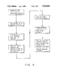
- FIGS. 5-8 show alternate methods of using a selected one of the punches shown in FIGS. 3 and 4 to produce the printed circuit board shown in FIGS. 1 and 2.
- FIGS. 1 and 2 show a printed circuit board, generally indicated at 10, which is constructed in accordance with the methods of this invention.
- the printed circuit board 10 includes a substrate 12 made from a suitable material such as a ceramic or an epoxy-glass material such as is now used on printed circuit boards of conventional construction.
- the substrate 12 may also be made of high temperature thermoplastic or thermosetting materials.
- the substrate 12 preferably has a relatively small thickness and substantially parallel planar surfaces.
- Grooves 14 are disposed in one or both of the parallel surfaces of the substrate 12.
- the grooves 14 are preferably provided with depths in the order of three thousandths of an inch (0.003") to twenty five thousandths of an inch (0.025”) but they may also be provided with different depths.
- the depth of the grooves is preferably at least as great as the width of the grooves.
- An electrically conductive material 16 such as solder is disposed in the grooves 14.
- the solder 16 may fill the grooves or partially fill the grooves or may be disposed essentially only on the walls of the grooves.
- Cavities 18 are also provided in one or both of the parallel surfaces of the substrate 12.
- the cavities 18 are provided with greater depths than the grooves 14.
- Electrical components are adapted to be disposed in the cavities 18, preferably in a tight fit with the walls of the cavities.
- the electrical components may include transistors such as a transistor 20, capacitors such as a capacitor 22 and resistors such as resistors 24.
- the electrical components such as the transistor 20, the capacitor 22 and the resistors 24 may be provided with electrical leads or may be constructed so as to have terminals without electrical leads. It will be appreciated that other electrical components may be disposed on the substrate above the planar surfaces of the boards.
- the grooves 14 are disposed to extend to the holes 18. In this way, the solder 16 in the grooves 14 establishes electrical continuity with the terminals or leads of the transistor 20, the capacitor 22 and the resistors 24. In the case of the transistor 20, the transistor is provided with a plurality of terminals or pads 26. The solder 16 is disposed in the grooves 16 to extend to the pads 26 and establish electrical continuity with the pads.
- the transistor 20 may generate a significant amount of heat in operation.
- a heat sink 28 may be disposed below the transistor in one of the cavities 18 to receive heat from the transistor 20 and thereby prevent the transistor from overheating.
- heat sinks may also be disposed below other components to facilitate the transfer of heat from these components and thereby prevent the components from overheating.
- the depths of the grooves 14 are preferably at least as great as the widths of the grooves and since the solder 16 can fill the grooves, the widths of the grooves can be made quite small while still retaining relatively low the electrical resistances of the leads formed by the solder.
- the size of the substrate 12 can accordingly be reduced in comparison to the size of the substrates which have previously been used.
- additional circuitry can be disposed on the substrate 12 by using the techniques of this invention. This is particularly true when it is considered that the provision of the cavities 18 in the substrate 12 and the disposition of the electrical components in the holes facilitate a compact arrangement of the electrical circuitry in and on the substrate.
- the components such as the transistor 20, the capacitor 22 and the resistors 24 can be disposed horizontally or vertically in the cavities 18.
- a vertical disposition facilitates a connection of one terminal of the component at a first surface of the substrate and a connection of another (or the other) terminal of the component at the other surface of the substrate.
- a horizontal disposition of the component facilitates the connection of the terminals of the component at the same surface of the substrate 12.
- the provision of the electrical circuitry in and on the substrate 12 is simplified in comparison to the prior art. Furthermore, the structural integrity of the connections to the components is enhanced. This may be seen from the fact that, in the prior art, electrical leads have to be bonded to the different components on the substrate. This is time consuming. Furthermore, the chances of an improper connection are considerably magnified in the methods of the prior art when considered in relation to the methods of this invention. The difficulties and disadvantages of the methods of the prior art become especially aggravating when connections are made to a component such as a transistor since the transistor is small and has a considerably number of closely spaced electrical terminals such as the pads 26.
- the grooves 14 and the cavities 18 can be formed by a number of different methods, all within the scope of the invention.
- a punch 30 is provided with a planar surface 31 and with raised portions 32 which are disposed and shaped to provide the grooves 14 and the holes 18 in the substrate 12.
- the punch 30 is heated to an elevated temperature dependent upon the characteristics of the material forming the substrate 12 and is then pressed against the substrate. The combination of the heat and pressure causes the substrate 12 to be deformed so that the grooves 14 and the cavities 18 are formed in the substrate.
- the substrate 12 may also be heated to facilitate the deformation of the substrate when the punch 30 is applied against the substrate.
- the punch 30 is removed from the substrate. Electrical components such as the transistor 20, the capacitor 22 and the resistors 24 may be disposed in the cavities 18 and solder 16 may be disposed in the grooves to communicate electrically with the electrical components. If desired, other electrical components may be disposed on the substrate 12 and may be connected to the solder 16 in the grooves to complete the electrical circuitry.
- a method as shown in FIG. 4 is provided for producing the printed circuit board 10.
- a mask is disposed on the punch 30.
- the punch 30 may be made from any material suitable for plating or the application of photosensitive or photoresist material.
- the punch 30 may be made from steel or copper.
- the mask 40 may be made from a photosensitive material which is well known in the art of printed circuitry.
- the thickness of the photosensitive mask 30 may be in the order of three thousandths of an inch (0.003") to twenty five thousandths of an inch (0.025") to provide the grooves 30.
- An image of the grooves 14 and the cavities 18 is then photoexposed on the mask 30.
- the techniques of, and the materials for, photoexposing the image of the grooves 14 and the cavities 18 on the mask 40 are well known in the art.
- the photoexposed portions of the mask 40 are then etched from the mask by materials and methods well known in the art to produce cavities in the mask at the positions of the grooves 14 and the holes 18 in the substrate 12.
- the cavities at the positions of the cavities may be machined to increase the depths of the cavities.
- the cavities in the mask 40 are subsequently filled by plating the punch 30 with a material, such as a metal, suitable for hot forming.
- a material such as a metal, suitable for hot forming.
- Plating materials well known in the art may be used. The plating may be accomplished by methods well known in the art. Typical plating materials may be nickel, copper, steel and/or chromium but other metals may also be used. The plating is controlled so that the plating material fills the cavities in the mask 40 to a level where the material is flush with the surface of the mask.
- the remaining portions of the mask 40 are now removed by materials and methods well known in the field of printed circuitry. In this way, only the plating materials discussed in the previous paragraph remain on the punch 30.
- the punch 30 is then heated to an elevated temperature dependent upon the material of the substrate 12. As will be appreciated, this elevated temperature is below the melting temperature of the material forming the substrate 12. Preferably the elevated temperature approaches the melting temperature of the substrate 12 to facilitate the deformation of the substrate by the punch 30 such that the grooves 14 and the cavities 18 are formed.
- the substrate 12 can be heated to an elevated temperature.
- This elevated temperature is below the melting temperature of the substrate 12 but approaches the melting temperature of the substrate to facilitate the deformation of the substrate by the punch for the formation of the grooves 14 and the cavities 18.
- the punch 30 is applied to the substrate to deform the substrate and produce the grooves 14 and the cavities 18.
- the punch 30 may be applied with some force to the substrate 12 to produce the grooves 14 and the cavities 18.
- the punch 30 is then removed from the substrate 12.
- the electrical components such as the transistor 20, the capacitor 22 and the resistors 24 are thereafter disposed in the associated ones of the cavities 18 in the substrate.
- An electrically conductive material such as the solder 16 is subsequently disposed in the grooves 18 to communicate electrically with other grooves and with the electrical components.
- the disposition of the solder 16 preferably occurs with the solder in molten form.
- the solder can be disposed in the grooves 14 by techniques well known in the art.
- the solder can fill the grooves 14 or partially fill the grooves or be disposed only against the walls of the grooves.
- electrical components may be externally disposed on the substrate 12 and may be connected to different electrical leads represented by the solder in the individual grooves.
- FIG. 6 sets forth the steps in an alternate method included within this invention.
- the projections for producing the grooves 14 and the cavities 18 in the substrate 12 may be produced in a punch as by machining.
- the punch is then heated and, alternatively or as an additional step, the substrate 12 may also be heated. While the punch and/or the substrate 12 are at an elevated temperature, the punch is then applied to the substrate 12 to form the grooves 14 and the cavities 18.
- the electrical components are disposed in the cavities 18 in the substrate and solder 16 is disposed in the grooves 14 in the substrate.
- FIG. 7 illustrates another alternative method included within this invention.
- a flat plate made from a suitable material such as copper, steel or nickel is attached to a punch.
- the plate is then coated with a photoresist material in a pattern corresponding to the pattern of the grooves 14 and the cavities 18 in the substrate 12.
- the coating of the plate with a photoresist material is well known in the art.
- the portions of the plate without the photoresist material are then removed from the plate by materials and methods well known in the art.
- the photoresist material on the plate is thereafter hardened by techniques well known in the art.
- the punch is provided with plated material, hardened, in a pattern corresponding to the pattern of the grooves 14 and the cavities 18 in the substrate 12.
- the remaining steps in the method shown in FIG. 7 correspond to steps in the method shown in FIG. 5 and discussed above.
- the punch and/or the substrate 12 are heated to an elevated temperature.
- the punch is then applied to the substrate 12 to form the grooves 14 and the holes 18 in the substrate.
- the punch is removed and the electrical components are inserted into the cavities 18 in the substrate 12.
- the grooves 14 are subsequently filled or at least partially filled with the solder 16 to establish electrical continuity with the components.
- the punch produced after the removal of the undesired portions of the plate may be used to make a female mold with a pattern inverse to the pattern of the portion of the plate remaining on the punch.
- a final tool may be made from the female mold for application against the substrate 12 to form the grooves 14 and the cavities 18 in the substrate.
- FIG. 8 still another method is shown which is included within this invention.
- a punch 50 is provided with raised portions 52 corresponding to the grooves 14 and the holes 16 in the substrate.
- the raised portions 52 may be provided in the punch by any of the methods discussed above.
- a metal foil 54 may be then disposed on the punch to conform to the surface of the punch including the raised portions on the surface of the punch. Such conformation may be provided by disposing elastomeric material on the workpiece which presses the metal foil on the punch and by pressing the workpiece against the punch such that the elastomeric material presses against the foil.
- the punch 50 and/or the metal foil 54 are then heated to an elevated temperature as described above.
- the foil 54 is then pressed by the punch on and into the substrate 12 to form the grooves 14 and the cavities 18 in the substrate.
- the foil becomes embedded in the substrate and adhered to the substrate.
- the foil is then removed from the substrate as by machining or printed circuit techniques such that only the portions of the foil in the grooves 14 remain.
- the electrical components may then be disposed in the cavities 18.
- the foil 54 may be a suitable material such as copper. Because of this, the foil may constitute the electrical leads extending through the grooves 14 to establish electrical continuity with the electrical components in the cavities 18. Preferably, the grooves 14 are thereafter plated as with solder to insure that good electrical conductivity is established with the electrical components.
- the methods described above and shown in the drawings have certain important advantages.
- One advantage is that the grooves 14 and the cavities 18 can be formed in the substrate 12 by a single stamping operation. This stamping operation is facilitated by heating the punch and/or the substrate. Furthermore, since successive ones of the substrates 12 are made by the same punch, substantial duplication of the grooves 14 and the cavities 18 in the successive ones of the substrates 12 is assured.
- the punch can be formed to define the grooves 14 and the holes 18 with great precision. In this way, printed circuit boards can be produced quickly and inexpensively with great precision in the location of electrical components and electrical leads and with optimal assurance that the electrical leads establish electrical continuity with the electrical components.
Abstract
Description
Claims (19)
Priority Applications (1)
| Application Number | Priority Date | Filing Date | Title |
|---|---|---|---|
| US07/230,460 US4912844A (en) | 1988-08-10 | 1988-08-10 | Methods of producing printed circuit boards |
Applications Claiming Priority (1)
| Application Number | Priority Date | Filing Date | Title |
|---|---|---|---|
| US07/230,460 US4912844A (en) | 1988-08-10 | 1988-08-10 | Methods of producing printed circuit boards |
Publications (1)
| Publication Number | Publication Date |
|---|---|
| US4912844A true US4912844A (en) | 1990-04-03 |
Family
ID=22865311
Family Applications (1)
| Application Number | Title | Priority Date | Filing Date |
|---|---|---|---|
| US07/230,460 Expired - Lifetime US4912844A (en) | 1988-08-10 | 1988-08-10 | Methods of producing printed circuit boards |
Country Status (1)
| Country | Link |
|---|---|
| US (1) | US4912844A (en) |
Cited By (47)
| Publication number | Priority date | Publication date | Assignee | Title |
|---|---|---|---|---|
| EP0626124A1 (en) * | 1992-02-14 | 1994-11-30 | Rock Ltd Partnership | High density conductive networks and method and apparatus for making same |
| US5584120A (en) * | 1992-02-14 | 1996-12-17 | Research Organization For Circuit Knowledge | Method of manufacturing printed circuits |
| US5718789A (en) * | 1995-06-07 | 1998-02-17 | The Dexter Corporation | Method for making a debossed conductive film composite |
| US5731086A (en) * | 1995-06-07 | 1998-03-24 | Gebhardt; William F. | Debossable films |
| US5761801A (en) * | 1995-06-07 | 1998-06-09 | The Dexter Corporation | Method for making a conductive film composite |
| EP0871568A1 (en) * | 1995-06-07 | 1998-10-21 | The Dexter Corporation | Conductive film composite |
| US5950305A (en) * | 1992-02-14 | 1999-09-14 | Research Organization For Circuit Knowledge | Environmentally desirable method of manufacturing printed circuits |
| US6083837A (en) * | 1996-12-13 | 2000-07-04 | Tessera, Inc. | Fabrication of components by coining |
| EP1019986A1 (en) * | 1997-10-07 | 2000-07-19 | Dimensional Circuits Corp. | Wiring board constructions and methods of making same |
| US6160714A (en) * | 1997-12-31 | 2000-12-12 | Elpac (Usa), Inc. | Molded electronic package and method of preparation |
| US6212072B1 (en) | 1999-05-19 | 2001-04-03 | Sagem Sa | Electronics package on a plate, and a method of making such a package |
| US6219253B1 (en) | 1997-12-31 | 2001-04-17 | Elpac (Usa), Inc. | Molded electronic package, method of preparation using build up technology and method of shielding |
| WO2001050825A1 (en) * | 2000-01-04 | 2001-07-12 | Elmicron Ag | Method, facility and device for producing an electrical connecting element, electrical connecting element and semi-finished product |
| US20030062123A1 (en) * | 2001-09-28 | 2003-04-03 | Hrl Laboratories, Llc | Method of self-latching for adhesion during self-assembly of electronic or optical components |
| US20030068519A1 (en) * | 2001-09-28 | 2003-04-10 | Hrl Laboratories, Llc | Method for assembly of complementary-shaped receptacle site and device microstructures |
| US20030112576A1 (en) * | 2001-09-28 | 2003-06-19 | Brewer Peter D. | Process for producing high performance interconnects |
| US20040118594A1 (en) * | 2002-12-18 | 2004-06-24 | Intel Corporation | Imprinted substrate and methods of manufacture |
| US20040118604A1 (en) * | 2002-12-18 | 2004-06-24 | Intel Corporation | Substrate-imprinting apparatus, methods of manufacture, and products formed therefrom |
| US20040124533A1 (en) * | 2002-12-31 | 2004-07-01 | Milan Keser | Method of semi-additive plating of imprinted layers and resulting product |
| US20040126547A1 (en) * | 2002-12-31 | 2004-07-01 | Coomer Boyd L. | Methods for performing substrate imprinting using thermoset resin varnishes and products formed therefrom |
| US20040142575A1 (en) * | 2002-07-25 | 2004-07-22 | Brewer Peter D. | Large area printing method for integrating device and circuit components |
| US20040176924A1 (en) * | 2003-03-07 | 2004-09-09 | Salmon Peter C. | Apparatus and method for testing electronic systems |
| US20050006335A1 (en) * | 2003-07-07 | 2005-01-13 | Christopher Wargo | Method of forming high resolution electronic circuits on a substrate |
| US20050040513A1 (en) * | 2003-08-20 | 2005-02-24 | Salmon Peter C. | Copper-faced modules, imprinted copper circuits, and their application to supercomputers |
| US20050064652A1 (en) * | 2003-08-08 | 2005-03-24 | Shmuel Shapira | Circuit forming system and method |
| US6916550B2 (en) | 2000-09-11 | 2005-07-12 | Allison Advanced Development Company | Method of manufacturing a metal matrix composite structure |
| US20050186712A1 (en) * | 1993-12-17 | 2005-08-25 | The Regents Of The University Of California | Method and apparatus for fabricating self-assembling microstructures |
| US20050183589A1 (en) * | 2004-02-19 | 2005-08-25 | Salmon Peter C. | Imprinting tools and methods for printed circuit boards and assemblies |
| US20050184376A1 (en) * | 2004-02-19 | 2005-08-25 | Salmon Peter C. | System in package |
| US20050255722A1 (en) * | 2004-05-07 | 2005-11-17 | Salmon Peter C | Micro blade assembly |
| US20060024900A1 (en) * | 2004-07-29 | 2006-02-02 | Lee Teck K | Interposer including at least one passive element at least partially defined by a recess formed therein, method of manufacture, system including same, and wafer-scale interposer |
| US20060037777A1 (en) * | 2004-07-12 | 2006-02-23 | Alps Electric Co., Ltd. | Mounting structure of electronic components and mounting method thereof |
| US20060160276A1 (en) * | 2002-12-14 | 2006-07-20 | Brown Thomas M | Electronic devices |
| US20060240360A1 (en) * | 2005-04-20 | 2006-10-26 | Samsung Electro-Mechanics Co., Ltd. | Method of manufacturing printed circuit board using imprinting process |
| US20070007983A1 (en) * | 2005-01-06 | 2007-01-11 | Salmon Peter C | Semiconductor wafer tester |
| US20070023904A1 (en) * | 2005-08-01 | 2007-02-01 | Salmon Peter C | Electro-optic interconnection apparatus and method |
| US20070023889A1 (en) * | 2005-08-01 | 2007-02-01 | Salmon Peter C | Copper substrate with feedthroughs and interconnection circuits |
| US20070023923A1 (en) * | 2005-08-01 | 2007-02-01 | Salmon Peter C | Flip chip interface including a mixed array of heat bumps and signal bumps |
| US7223635B1 (en) | 2003-07-25 | 2007-05-29 | Hrl Laboratories, Llc | Oriented self-location of microstructures with alignment structures |
| US7253091B2 (en) | 2001-09-28 | 2007-08-07 | Hrl Laboratories, Llc | Process for assembling three-dimensional systems on a chip and structure thus obtained |
| US7334326B1 (en) * | 2001-06-19 | 2008-02-26 | Amkor Technology, Inc. | Method for making an integrated circuit substrate having embedded passive components |
| US7427809B2 (en) | 2004-12-16 | 2008-09-23 | Salmon Technologies, Llc | Repairable three-dimensional semiconductor subsystem |
| US20090193652A1 (en) * | 2005-08-01 | 2009-08-06 | Salmon Peter C | Scalable subsystem architecture having integrated cooling channels |
| DE102009006181A1 (en) | 2009-01-27 | 2010-07-29 | Via Electronic Gmbh | Printed circuit or electronic component e.g. coil, manufacturing method, involves applying contours of conducting paths or component elements on ceramic substrate by silver paste, such that geometrical structures are formed on substrate |
| US7875952B1 (en) | 2006-09-19 | 2011-01-25 | Hrl Laboratories, Llc | Method of transistor level heterogeneous integration and system |
| US20110119912A1 (en) * | 2004-06-30 | 2011-05-26 | Choi Kyoung-Sei | Method for manufacturing tape wiring board |
| US11562984B1 (en) | 2020-10-14 | 2023-01-24 | Hrl Laboratories, Llc | Integrated mechanical aids for high accuracy alignable-electrical contacts |
Citations (6)
| Publication number | Priority date | Publication date | Assignee | Title |
|---|---|---|---|---|
| US2955351A (en) * | 1954-12-28 | 1960-10-11 | Plast O Fab Circuits Inc | Method of making a printed circuit |
| US2986804A (en) * | 1957-02-06 | 1961-06-06 | Rogers Corp | Method of making a printed circuit |
| US3990142A (en) * | 1973-10-02 | 1976-11-09 | Jerobee Industries, Inc. | Circuit board, method of making the circuit board and improved die for making said board |
| US4363930A (en) * | 1980-02-04 | 1982-12-14 | Amp Incorporated | Circuit path conductors in plural planes |
| US4374457A (en) * | 1980-08-04 | 1983-02-22 | Wiech Raymond E Jr | Method of fabricating complex micro-circuit boards and substrates |
| US4614837A (en) * | 1985-04-03 | 1986-09-30 | Allied Corporation | Method for placing electrically conductive paths on a substrate |
-
1988
- 1988-08-10 US US07/230,460 patent/US4912844A/en not_active Expired - Lifetime
Patent Citations (6)
| Publication number | Priority date | Publication date | Assignee | Title |
|---|---|---|---|---|
| US2955351A (en) * | 1954-12-28 | 1960-10-11 | Plast O Fab Circuits Inc | Method of making a printed circuit |
| US2986804A (en) * | 1957-02-06 | 1961-06-06 | Rogers Corp | Method of making a printed circuit |
| US3990142A (en) * | 1973-10-02 | 1976-11-09 | Jerobee Industries, Inc. | Circuit board, method of making the circuit board and improved die for making said board |
| US4363930A (en) * | 1980-02-04 | 1982-12-14 | Amp Incorporated | Circuit path conductors in plural planes |
| US4374457A (en) * | 1980-08-04 | 1983-02-22 | Wiech Raymond E Jr | Method of fabricating complex micro-circuit boards and substrates |
| US4614837A (en) * | 1985-04-03 | 1986-09-30 | Allied Corporation | Method for placing electrically conductive paths on a substrate |
Cited By (88)
| Publication number | Priority date | Publication date | Assignee | Title |
|---|---|---|---|---|
| US5950305A (en) * | 1992-02-14 | 1999-09-14 | Research Organization For Circuit Knowledge | Environmentally desirable method of manufacturing printed circuits |
| EP0626124A4 (en) * | 1992-02-14 | 1995-11-15 | Rock Lp | High density conductive networks and method and apparatus for making same. |
| US5584120A (en) * | 1992-02-14 | 1996-12-17 | Research Organization For Circuit Knowledge | Method of manufacturing printed circuits |
| KR100298010B1 (en) * | 1992-02-14 | 2001-11-22 | ||
| EP0626124A1 (en) * | 1992-02-14 | 1994-11-30 | Rock Ltd Partnership | High density conductive networks and method and apparatus for making same |
| US7229848B2 (en) * | 1993-12-17 | 2007-06-12 | The Regents Of The University Of California | Method and apparatus for fabricating self-assembling microstructures |
| US20100075463A1 (en) * | 1993-12-17 | 2010-03-25 | The Regents Of The University Of California | Method and apparatus for fabricating self-assembling microstructures |
| US7727804B2 (en) | 1993-12-17 | 2010-06-01 | The Regents Of The University Of California | Method and apparatus for fabricating self-assembling microstructures |
| US20050186712A1 (en) * | 1993-12-17 | 2005-08-25 | The Regents Of The University Of California | Method and apparatus for fabricating self-assembling microstructures |
| US5731086A (en) * | 1995-06-07 | 1998-03-24 | Gebhardt; William F. | Debossable films |
| EP0836795A4 (en) * | 1995-06-07 | 2000-05-10 | Dexter Corp | Method for making a debossed conductive film composite |
| US5928767A (en) * | 1995-06-07 | 1999-07-27 | Dexter Corporation | Conductive film composite |
| EP0871568A1 (en) * | 1995-06-07 | 1998-10-21 | The Dexter Corporation | Conductive film composite |
| US5761801A (en) * | 1995-06-07 | 1998-06-09 | The Dexter Corporation | Method for making a conductive film composite |
| EP0836795A1 (en) * | 1995-06-07 | 1998-04-22 | The Dexter Corporation | Method for making a debossed conductive film composite |
| US5718789A (en) * | 1995-06-07 | 1998-02-17 | The Dexter Corporation | Method for making a debossed conductive film composite |
| EP0871568A4 (en) * | 1995-06-07 | 2002-05-08 | Dexter Corp | Conductive film composite |
| US6184140B1 (en) | 1996-12-13 | 2001-02-06 | Tessera, Inc. | Methods of making microelectronic packages utilizing coining |
| US6083837A (en) * | 1996-12-13 | 2000-07-04 | Tessera, Inc. | Fabrication of components by coining |
| EP1019986A4 (en) * | 1997-10-07 | 2003-03-26 | Dimensional Circuits Corp | Wiring board constructions and methods of making same |
| EP1019986A1 (en) * | 1997-10-07 | 2000-07-19 | Dimensional Circuits Corp. | Wiring board constructions and methods of making same |
| US6219253B1 (en) | 1997-12-31 | 2001-04-17 | Elpac (Usa), Inc. | Molded electronic package, method of preparation using build up technology and method of shielding |
| US6519161B1 (en) | 1997-12-31 | 2003-02-11 | William J. Green | Molded electronic package, method of preparation and method of shielding-II |
| US6160714A (en) * | 1997-12-31 | 2000-12-12 | Elpac (Usa), Inc. | Molded electronic package and method of preparation |
| US6212072B1 (en) | 1999-05-19 | 2001-04-03 | Sagem Sa | Electronics package on a plate, and a method of making such a package |
| WO2001050825A1 (en) * | 2000-01-04 | 2001-07-12 | Elmicron Ag | Method, facility and device for producing an electrical connecting element, electrical connecting element and semi-finished product |
| EP1320287A1 (en) * | 2000-01-04 | 2003-06-18 | Elmicron AG | Electrical connecting element and semi-finished product |
| US20030135998A1 (en) * | 2000-01-04 | 2003-07-24 | Silke Walz | Method, facility and device for producing an electrical connecting element, electrical connecting element and semi-finished product |
| US6916550B2 (en) | 2000-09-11 | 2005-07-12 | Allison Advanced Development Company | Method of manufacturing a metal matrix composite structure |
| US7334326B1 (en) * | 2001-06-19 | 2008-02-26 | Amkor Technology, Inc. | Method for making an integrated circuit substrate having embedded passive components |
| US7351660B2 (en) | 2001-09-28 | 2008-04-01 | Hrl Laboratories, Llc | Process for producing high performance interconnects |
| US6974604B2 (en) | 2001-09-28 | 2005-12-13 | Hrl Laboratories, Llc | Method of self-latching for adhesion during self-assembly of electronic or optical components |
| US7253091B2 (en) | 2001-09-28 | 2007-08-07 | Hrl Laboratories, Llc | Process for assembling three-dimensional systems on a chip and structure thus obtained |
| US20030062123A1 (en) * | 2001-09-28 | 2003-04-03 | Hrl Laboratories, Llc | Method of self-latching for adhesion during self-assembly of electronic or optical components |
| US20030068519A1 (en) * | 2001-09-28 | 2003-04-10 | Hrl Laboratories, Llc | Method for assembly of complementary-shaped receptacle site and device microstructures |
| US20030112576A1 (en) * | 2001-09-28 | 2003-06-19 | Brewer Peter D. | Process for producing high performance interconnects |
| US7018575B2 (en) | 2001-09-28 | 2006-03-28 | Hrl Laboratories, Llc | Method for assembly of complementary-shaped receptacle site and device microstructures |
| US6946322B2 (en) | 2002-07-25 | 2005-09-20 | Hrl Laboratories, Llc | Large area printing method for integrating device and circuit components |
| US20040142575A1 (en) * | 2002-07-25 | 2004-07-22 | Brewer Peter D. | Large area printing method for integrating device and circuit components |
| US7935565B2 (en) * | 2002-12-14 | 2011-05-03 | Plastic Logic Limited | Electronic devices |
| US20060160276A1 (en) * | 2002-12-14 | 2006-07-20 | Brown Thomas M | Electronic devices |
| US20110207300A1 (en) * | 2002-12-14 | 2011-08-25 | Plastic Logic Limited | Electronic devices |
| US20040118604A1 (en) * | 2002-12-18 | 2004-06-24 | Intel Corporation | Substrate-imprinting apparatus, methods of manufacture, and products formed therefrom |
| US20040118594A1 (en) * | 2002-12-18 | 2004-06-24 | Intel Corporation | Imprinted substrate and methods of manufacture |
| US7637008B2 (en) | 2002-12-18 | 2009-12-29 | Intel Corporation | Methods for manufacturing imprinted substrates |
| US7371975B2 (en) | 2002-12-18 | 2008-05-13 | Intel Corporation | Electronic packages and components thereof formed by substrate-imprinting |
| US20080000674A1 (en) * | 2002-12-18 | 2008-01-03 | Intel Corporation | Substrate-imprinting apparatus and methods |
| US7594321B2 (en) | 2002-12-18 | 2009-09-29 | Intel Corporation | Substrate-imprinting methods |
| US6974775B2 (en) | 2002-12-31 | 2005-12-13 | Intel Corporation | Method and apparatus for making an imprinted conductive circuit using semi-additive plating |
| US20040126547A1 (en) * | 2002-12-31 | 2004-07-01 | Coomer Boyd L. | Methods for performing substrate imprinting using thermoset resin varnishes and products formed therefrom |
| US20040124533A1 (en) * | 2002-12-31 | 2004-07-01 | Milan Keser | Method of semi-additive plating of imprinted layers and resulting product |
| US7505862B2 (en) | 2003-03-07 | 2009-03-17 | Salmon Technologies, Llc | Apparatus and method for testing electronic systems |
| US20090192753A1 (en) * | 2003-03-07 | 2009-07-30 | Salmon Peter C | Apparatus and method for testing electronic systems |
| US20040176924A1 (en) * | 2003-03-07 | 2004-09-09 | Salmon Peter C. | Apparatus and method for testing electronic systems |
| US20060118233A1 (en) * | 2003-07-07 | 2006-06-08 | Christopher Wargo | System and method for forming high resolution electronic circuits on a substrate |
| US7014727B2 (en) | 2003-07-07 | 2006-03-21 | Potomac Photonics, Inc. | Method of forming high resolution electronic circuits on a substrate |
| US20050006335A1 (en) * | 2003-07-07 | 2005-01-13 | Christopher Wargo | Method of forming high resolution electronic circuits on a substrate |
| US7622813B2 (en) | 2003-07-25 | 2009-11-24 | Hrl Laboratories, Llc | Oriented self-location of microstructures with alignment structures |
| US20070252289A1 (en) * | 2003-07-25 | 2007-11-01 | Hrl Laboratories, Llc | Oriented self-location of microstructures with alignment structures |
| US7223635B1 (en) | 2003-07-25 | 2007-05-29 | Hrl Laboratories, Llc | Oriented self-location of microstructures with alignment structures |
| US20050064652A1 (en) * | 2003-08-08 | 2005-03-24 | Shmuel Shapira | Circuit forming system and method |
| US7152317B2 (en) * | 2003-08-08 | 2006-12-26 | Shmuel Shapira | Circuit forming method |
| US7408258B2 (en) | 2003-08-20 | 2008-08-05 | Salmon Technologies, Llc | Interconnection circuit and electronic module utilizing same |
| US20050040513A1 (en) * | 2003-08-20 | 2005-02-24 | Salmon Peter C. | Copper-faced modules, imprinted copper circuits, and their application to supercomputers |
| US20050184376A1 (en) * | 2004-02-19 | 2005-08-25 | Salmon Peter C. | System in package |
| US20050183589A1 (en) * | 2004-02-19 | 2005-08-25 | Salmon Peter C. | Imprinting tools and methods for printed circuit boards and assemblies |
| US20050255722A1 (en) * | 2004-05-07 | 2005-11-17 | Salmon Peter C | Micro blade assembly |
| US20110119912A1 (en) * | 2004-06-30 | 2011-05-26 | Choi Kyoung-Sei | Method for manufacturing tape wiring board |
| US8250750B2 (en) * | 2004-06-30 | 2012-08-28 | Samsung Electronics Co., Ltd. | Method for manufacturing tape wiring board |
| US20060037777A1 (en) * | 2004-07-12 | 2006-02-23 | Alps Electric Co., Ltd. | Mounting structure of electronic components and mounting method thereof |
| US7621042B2 (en) * | 2004-07-12 | 2009-11-24 | Alps Electric Co., Ltd. | Method for mounting electronic components on a substrate |
| US7663206B2 (en) | 2004-07-29 | 2010-02-16 | Micron Tachnology, Inc. | Interposer including at least one passive element at least partially defined by a recess formed therein, system including same, and wafer-scale interposer |
| US20060024900A1 (en) * | 2004-07-29 | 2006-02-02 | Lee Teck K | Interposer including at least one passive element at least partially defined by a recess formed therein, method of manufacture, system including same, and wafer-scale interposer |
| US7494889B2 (en) | 2004-07-29 | 2009-02-24 | Micron Technology, Inc. | Method of manufacturing an interposer including at least one passive element at least partially defined by a recess therein |
| US20060125047A1 (en) * | 2004-07-29 | 2006-06-15 | Lee Teck K | Interposer including at least one passive element at least partially defined by a recess formed therein, system including same, and wafer-scale interposer |
| US7427809B2 (en) | 2004-12-16 | 2008-09-23 | Salmon Technologies, Llc | Repairable three-dimensional semiconductor subsystem |
| US20070007983A1 (en) * | 2005-01-06 | 2007-01-11 | Salmon Peter C | Semiconductor wafer tester |
| US7666292B2 (en) | 2005-04-20 | 2010-02-23 | Samsung Electro-Mechanics Co., Ltd. | Method of manufacturing printed circuit board using imprinting process |
| US20060240360A1 (en) * | 2005-04-20 | 2006-10-26 | Samsung Electro-Mechanics Co., Ltd. | Method of manufacturing printed circuit board using imprinting process |
| US20070023889A1 (en) * | 2005-08-01 | 2007-02-01 | Salmon Peter C | Copper substrate with feedthroughs and interconnection circuits |
| US20070023904A1 (en) * | 2005-08-01 | 2007-02-01 | Salmon Peter C | Electro-optic interconnection apparatus and method |
| US20090193652A1 (en) * | 2005-08-01 | 2009-08-06 | Salmon Peter C | Scalable subsystem architecture having integrated cooling channels |
| US20070023923A1 (en) * | 2005-08-01 | 2007-02-01 | Salmon Peter C | Flip chip interface including a mixed array of heat bumps and signal bumps |
| US7586747B2 (en) | 2005-08-01 | 2009-09-08 | Salmon Technologies, Llc. | Scalable subsystem architecture having integrated cooling channels |
| US7875952B1 (en) | 2006-09-19 | 2011-01-25 | Hrl Laboratories, Llc | Method of transistor level heterogeneous integration and system |
| DE102009006181A1 (en) | 2009-01-27 | 2010-07-29 | Via Electronic Gmbh | Printed circuit or electronic component e.g. coil, manufacturing method, involves applying contours of conducting paths or component elements on ceramic substrate by silver paste, such that geometrical structures are formed on substrate |
| DE102009006181B4 (en) * | 2009-01-27 | 2021-06-24 | Via Electronic Gmbh | Process for the production of printed circuits or electronic components of this type |
| US11562984B1 (en) | 2020-10-14 | 2023-01-24 | Hrl Laboratories, Llc | Integrated mechanical aids for high accuracy alignable-electrical contacts |
Similar Documents
| Publication | Publication Date | Title |
|---|---|---|
| US4912844A (en) | Methods of producing printed circuit boards | |
| US4985601A (en) | Circuit boards with recessed traces | |
| US5055637A (en) | Circuit boards with recessed traces | |
| US5457881A (en) | Method for the through plating of conductor foils | |
| US5972140A (en) | Method of fabricating multilayer structures with nonplanar surfaces | |
| JP4129971B2 (en) | Wiring board manufacturing method | |
| US5305523A (en) | Method of direct transferring of electrically conductive elements into a substrate | |
| US2925645A (en) | Process for forming an insulation backed wiring panel | |
| US3013188A (en) | Mechanically integrated circuit board and a method of making same by die forms | |
| US5146674A (en) | Manufacturing process of a high density substrate design | |
| US3680209A (en) | Method of forming stacked circuit boards | |
| US4969257A (en) | Transfer sheet and process for making a circuit substrate | |
| EP1267595A4 (en) | Circuit forming board producing method, circuit forming board, and material for circuit forming board | |
| US3060076A (en) | Method of making bases for printed electric circuits | |
| JP3806294B2 (en) | Circuit board manufacturing method | |
| US5296082A (en) | Mold for printed wiring board | |
| WO1984003586A1 (en) | Method for bonding electrical conductors to an insulating substrate | |
| KR20050065289A (en) | Semiconductor multilayer wiring substrate of coaxial wiring structure and method of fabricating the same | |
| JPH0239879B2 (en) | ||
| EP1269808B1 (en) | Method for fabricating electrical connecting elements, and connecting element | |
| US4889962A (en) | Circuit board with coaxial circuit and method therefor | |
| JP2675985B2 (en) | Transfer board for circuit board manufacturing | |
| JP3948317B2 (en) | Method for manufacturing thermally conductive substrate | |
| JPH0774451A (en) | Manufacture of circuit board | |
| WO1999057951A1 (en) | A printed circuit board and a method of processing printed circuit boards |
Legal Events
| Date | Code | Title | Description |
|---|---|---|---|
| AS | Assignment |
Owner name: DIMENSIONAL CIRCUITS CORPORATION, 10660 SCRIPPS RA Free format text: ASSIGNMENT OF ASSIGNORS INTEREST.;ASSIGNOR:PARKER, FREDERICK;REEL/FRAME:004921/0367 Effective date: 19880730 |
|
| STCF | Information on status: patent grant |
Free format text: PATENTED CASE |
|
| FEPP | Fee payment procedure |
Free format text: PAYOR NUMBER ASSIGNED (ORIGINAL EVENT CODE: ASPN); ENTITY STATUS OF PATENT OWNER: SMALL ENTITY |
|
| FPAY | Fee payment |
Year of fee payment: 4 |
|
| FEPP | Fee payment procedure |
Free format text: PAYOR NUMBER ASSIGNED (ORIGINAL EVENT CODE: ASPN); ENTITY STATUS OF PATENT OWNER: SMALL ENTITY Free format text: PAYER NUMBER DE-ASSIGNED (ORIGINAL EVENT CODE: RMPN); ENTITY STATUS OF PATENT OWNER: SMALL ENTITY |
|
| FPAY | Fee payment |
Year of fee payment: 8 |
|
| FPAY | Fee payment |
Year of fee payment: 12 |