US4960719A - Method for producing amorphous silicon thin film transistor array substrate - Google Patents
Method for producing amorphous silicon thin film transistor array substrate Download PDFInfo
- Publication number
- US4960719A US4960719A US07/300,629 US30062989A US4960719A US 4960719 A US4960719 A US 4960719A US 30062989 A US30062989 A US 30062989A US 4960719 A US4960719 A US 4960719A
- Authority
- US
- United States
- Prior art keywords
- gate wiring
- layer
- insulating layer
- amorphous silicon
- gate
- Prior art date
- Legal status (The legal status is an assumption and is not a legal conclusion. Google has not performed a legal analysis and makes no representation as to the accuracy of the status listed.)
- Expired - Lifetime
Links
- 229910021417 amorphous silicon Inorganic materials 0.000 title claims abstract description 55
- 239000000758 substrate Substances 0.000 title claims abstract description 43
- 238000004519 manufacturing process Methods 0.000 title claims abstract description 28
- 239000010409 thin film Substances 0.000 title claims abstract description 8
- 239000011521 glass Substances 0.000 claims abstract description 37
- 230000001681 protective effect Effects 0.000 claims abstract description 29
- 229920002120 photoresistant polymer Polymers 0.000 claims abstract description 15
- 239000011248 coating agent Substances 0.000 claims abstract description 3
- 238000000576 coating method Methods 0.000 claims abstract description 3
- 238000005530 etching Methods 0.000 claims description 12
- 238000000059 patterning Methods 0.000 claims description 4
- 239000002184 metal Substances 0.000 description 37
- 238000000034 method Methods 0.000 description 22
- 229910052581 Si3N4 Inorganic materials 0.000 description 15
- VYPSYNLAJGMNEJ-UHFFFAOYSA-N Silicium dioxide Chemical compound O=[Si]=O VYPSYNLAJGMNEJ-UHFFFAOYSA-N 0.000 description 15
- 238000010586 diagram Methods 0.000 description 15
- HQVNEWCFYHHQES-UHFFFAOYSA-N silicon nitride Chemical compound N12[Si]34N5[Si]62N3[Si]51N64 HQVNEWCFYHHQES-UHFFFAOYSA-N 0.000 description 15
- 229910052814 silicon oxide Inorganic materials 0.000 description 15
- KRHYYFGTRYWZRS-UHFFFAOYSA-N Fluorane Chemical compound F KRHYYFGTRYWZRS-UHFFFAOYSA-N 0.000 description 9
- 229960002050 hydrofluoric acid Drugs 0.000 description 9
- 239000004973 liquid crystal related substance Substances 0.000 description 9
- 239000000243 solution Substances 0.000 description 9
- 230000000694 effects Effects 0.000 description 8
- 238000000151 deposition Methods 0.000 description 5
- 239000011159 matrix material Substances 0.000 description 5
- 238000005268 plasma chemical vapour deposition Methods 0.000 description 5
- 239000012670 alkaline solution Substances 0.000 description 4
- 238000010276 construction Methods 0.000 description 3
- 238000007796 conventional method Methods 0.000 description 2
- 230000002093 peripheral effect Effects 0.000 description 2
- 230000015556 catabolic process Effects 0.000 description 1
- 230000003247 decreasing effect Effects 0.000 description 1
- 230000007547 defect Effects 0.000 description 1
- 230000002950 deficient Effects 0.000 description 1
- 230000008021 deposition Effects 0.000 description 1
- 238000009826 distribution Methods 0.000 description 1
- 239000000428 dust Substances 0.000 description 1
- 239000010408 film Substances 0.000 description 1
- BHEPBYXIRTUNPN-UHFFFAOYSA-N hydridophosphorus(.) (triplet) Chemical compound [PH] BHEPBYXIRTUNPN-UHFFFAOYSA-N 0.000 description 1
- 239000012535 impurity Substances 0.000 description 1
- 238000009413 insulation Methods 0.000 description 1
- 230000003287 optical effect Effects 0.000 description 1
- 238000012827 research and development Methods 0.000 description 1
- 239000000126 substance Substances 0.000 description 1
Images


Classifications
-
- H—ELECTRICITY
- H01—ELECTRIC ELEMENTS
- H01L—SEMICONDUCTOR DEVICES NOT COVERED BY CLASS H10
- H01L29/00—Semiconductor devices adapted for rectifying, amplifying, oscillating or switching, or capacitors or resistors with at least one potential-jump barrier or surface barrier, e.g. PN junction depletion layer or carrier concentration layer; Details of semiconductor bodies or of electrodes thereof ; Multistep manufacturing processes therefor
- H01L29/66—Types of semiconductor device ; Multistep manufacturing processes therefor
- H01L29/68—Types of semiconductor device ; Multistep manufacturing processes therefor controllable by only the electric current supplied, or only the electric potential applied, to an electrode which does not carry the current to be rectified, amplified or switched
-
- H—ELECTRICITY
- H01—ELECTRIC ELEMENTS
- H01L—SEMICONDUCTOR DEVICES NOT COVERED BY CLASS H10
- H01L27/00—Devices consisting of a plurality of semiconductor or other solid-state components formed in or on a common substrate
- H01L27/02—Devices consisting of a plurality of semiconductor or other solid-state components formed in or on a common substrate including semiconductor components specially adapted for rectifying, oscillating, amplifying or switching and having at least one potential-jump barrier or surface barrier; including integrated passive circuit elements with at least one potential-jump barrier or surface barrier
- H01L27/12—Devices consisting of a plurality of semiconductor or other solid-state components formed in or on a common substrate including semiconductor components specially adapted for rectifying, oscillating, amplifying or switching and having at least one potential-jump barrier or surface barrier; including integrated passive circuit elements with at least one potential-jump barrier or surface barrier the substrate being other than a semiconductor body, e.g. an insulating body
- H01L27/1214—Devices consisting of a plurality of semiconductor or other solid-state components formed in or on a common substrate including semiconductor components specially adapted for rectifying, oscillating, amplifying or switching and having at least one potential-jump barrier or surface barrier; including integrated passive circuit elements with at least one potential-jump barrier or surface barrier the substrate being other than a semiconductor body, e.g. an insulating body comprising a plurality of TFTs formed on a non-semiconducting substrate, e.g. driving circuits for AMLCDs
- H01L27/124—Devices consisting of a plurality of semiconductor or other solid-state components formed in or on a common substrate including semiconductor components specially adapted for rectifying, oscillating, amplifying or switching and having at least one potential-jump barrier or surface barrier; including integrated passive circuit elements with at least one potential-jump barrier or surface barrier the substrate being other than a semiconductor body, e.g. an insulating body comprising a plurality of TFTs formed on a non-semiconducting substrate, e.g. driving circuits for AMLCDs with a particular composition, shape or layout of the wiring layers specially adapted to the circuit arrangement, e.g. scanning lines in LCD pixel circuits
- H01L27/1244—Devices consisting of a plurality of semiconductor or other solid-state components formed in or on a common substrate including semiconductor components specially adapted for rectifying, oscillating, amplifying or switching and having at least one potential-jump barrier or surface barrier; including integrated passive circuit elements with at least one potential-jump barrier or surface barrier the substrate being other than a semiconductor body, e.g. an insulating body comprising a plurality of TFTs formed on a non-semiconducting substrate, e.g. driving circuits for AMLCDs with a particular composition, shape or layout of the wiring layers specially adapted to the circuit arrangement, e.g. scanning lines in LCD pixel circuits for preventing breakage, peeling or short circuiting
-
- H—ELECTRICITY
- H01—ELECTRIC ELEMENTS
- H01L—SEMICONDUCTOR DEVICES NOT COVERED BY CLASS H10
- H01L27/00—Devices consisting of a plurality of semiconductor or other solid-state components formed in or on a common substrate
- H01L27/02—Devices consisting of a plurality of semiconductor or other solid-state components formed in or on a common substrate including semiconductor components specially adapted for rectifying, oscillating, amplifying or switching and having at least one potential-jump barrier or surface barrier; including integrated passive circuit elements with at least one potential-jump barrier or surface barrier
- H01L27/12—Devices consisting of a plurality of semiconductor or other solid-state components formed in or on a common substrate including semiconductor components specially adapted for rectifying, oscillating, amplifying or switching and having at least one potential-jump barrier or surface barrier; including integrated passive circuit elements with at least one potential-jump barrier or surface barrier the substrate being other than a semiconductor body, e.g. an insulating body
- H01L27/1214—Devices consisting of a plurality of semiconductor or other solid-state components formed in or on a common substrate including semiconductor components specially adapted for rectifying, oscillating, amplifying or switching and having at least one potential-jump barrier or surface barrier; including integrated passive circuit elements with at least one potential-jump barrier or surface barrier the substrate being other than a semiconductor body, e.g. an insulating body comprising a plurality of TFTs formed on a non-semiconducting substrate, e.g. driving circuits for AMLCDs
- H01L27/1259—Multistep manufacturing methods
- H01L27/1288—Multistep manufacturing methods employing particular masking sequences or specially adapted masks, e.g. half-tone mask
-
- H—ELECTRICITY
- H01—ELECTRIC ELEMENTS
- H01L—SEMICONDUCTOR DEVICES NOT COVERED BY CLASS H10
- H01L29/00—Semiconductor devices adapted for rectifying, amplifying, oscillating or switching, or capacitors or resistors with at least one potential-jump barrier or surface barrier, e.g. PN junction depletion layer or carrier concentration layer; Details of semiconductor bodies or of electrodes thereof ; Multistep manufacturing processes therefor
- H01L29/66—Types of semiconductor device ; Multistep manufacturing processes therefor
- H01L29/68—Types of semiconductor device ; Multistep manufacturing processes therefor controllable by only the electric current supplied, or only the electric potential applied, to an electrode which does not carry the current to be rectified, amplified or switched
- H01L29/76—Unipolar devices, e.g. field effect transistors
- H01L29/772—Field effect transistors
- H01L29/78—Field effect transistors with field effect produced by an insulated gate
Definitions
- the present invention relates to a method for producing an amorphous silicon (hereinafter referred to as a-Si) thin film transistor (hereinafter referred to as TFT) array substrate.
- a-Si amorphous silicon
- TFT thin film transistor
- a liquid crystal matrix display device especially a liquid crystal display device of the so-called active matrix type provided with a switching element per each pixel has been under research and development in various places.
- a switching element an MIS type TFT using a-Si is mainly utilized.
- FIG. 7 schematically represents an example of the circuit construction of an active matrix type liquid crystal display device using TFT.
- the gates of respective TFT 13-a connected thereto are turned on all at once, and through the sources of these TFT turned on, the signal voltage corresponding to the picture information is transmitted from respective signal lines 12 to the drains of respective TFT 13-a.
- a pixel electrode (not shown in the Figure) is connected to the drain, and by the voltage difference between this pixel electrode and the counter electrode 15 formed on the substrate, which is on the other side, when putting the liquid crystal layer 14 between, the optical transparency of the liquid crystal layer 14 is changed to effect a picture image display.
- each TFT 13-a connected thereto When the Xi is in a non-selective state, the gate of each TFT 13-a connected thereto is turned off, and successively, Xi+1 is selected, and the gate of each TFT 13-b is turned on, and a process similar to that as described above is effected. Even after the gate was turned off, since the voltage difference between both the pixel electrode and the counter electrode 15 is preserved by the liquid crystal layer 14 until the same scanning line is selected the next time, the liquid crystal corresponding to each pixel becomes statically driven, and a display of high contrast can be obtained.
- the TFT produced by the production method having the process of successively depositing a gate insulating layer, an a-Si layer, and a protective insulating layer is hopeful from the viewpoint of reliability, reproducibility of the production method and the like.
- FIGS. 8(a) to 8(d) are diagrams schematically representing an example of the production method of the a-Si TFT used in an active matrix type liquid crystal display device, and having the above-described method of production. In the following, explanation will be given by referring to this Figure.
- a metal layer of Cr or the like is selectively formed by coating on a glass substrate 21, and a gate electrode 22 and gate wiring (not shown in the Figure) are formed thereon, and successively, a gate insulating layer 23 made of silicon nitride or silicon oxide, an intrinsic a-Si (hereinafter referred to as i-a-Si layer 24 containing almost no impurities which form an active layer, and a protective insulating layer 25 made of silicon nitride or silicon oxide are deposited by using, for example, a plasma CVD method.
- the protective insulating layer Z5 is selectively etched by use of a buffer fluoric acid solution to expose the i-a-Si layer 24 such as to make a part thereof overlap on the gate electrode 22.
- n-a-Si layer 26 An n-type a-Si (hereinafter referred to as an n-a-Si) layer 26 containing an appropriate amount of phosphorous and a metal layer 27 of Ti or the like are successively deposited, and the metal layer 27 is selectively etched and is patterned into the shape of source and drain electrodes, and using the metal layer 27 and the protective insulating layer 25 as a mask, the n-a-Si layer 26 and i-a-Si layer 24 are etched by use of an organic alkaline solution, and an island-like structure is formed.
- a transparent conductive layer 28 of ITO or the like is deposited, and by selectively removing it, a source wiring and a pixel electrode are formed.
- FIG. 10 schematically shows the status of the connecting terminal part at this time.
- Numeral 21 denotes a glass substrate, numeral 22 a gate wiring, numeral 23 a gate insulating layer, and numeral 24 an i-a-Si layer.
- the present invention has been carried out in view of the above-described defects, and has the main object of removing the roughness of the surface of the glass substrate or the under cut at the end part of the gate wiring or the like.
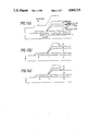
- FIGS. 1(a) to 1(c) are sectional diagrams showing the production method of the first embodiment of the present invention.
- FIGS. 2(a) to 2(c) are sectional diagrams showing the second embodiment.
- FIGS. 3(a) to 3(d) are sectional diagrams showing the third embodiment.
- FIG. 4 is a sectional diagram showing the fourth embodiment.
- FIG. 5 is a sectional diagram showing the fifth embodiment.
- FIG. 6 is a sectional diagram showing the sixth embodiment.
- FIG. 7 is an electric circuit diagram showing the principle of the active matrix type liquid crystal display device.
- FIGS. 8(a) to 8(d) are sectional diagrams showing one example of the production process of the amorphous silicon thin film transistor.
- FIG. 9 is a perspective diagram showing the relationship between the glass substrate and the metal mask.
- FIG. 10 is a sectional diagram showing the connecting terminal part of the gate wiring in a conventional production method.
- FIG. 1 is a diagram which shows the first embodiment of the present invention, and schematically shows the section of the connecting terminal part of the gate wiring.
- Numeral 1 denotes a glass substrate, numeral 2 a gate wiring, numeral 3 silicon nitride or silicon oxide for forming the gate insulating layer, numeral 4 an i-a-Si layer, numeral 5 silicon nitride or silicon oxide for forming the protective insulating layer, numeral 9 a connecting terminal, and numeral 10 the photoresist.
- a gate insulating layer 3 made of silicon nitride or silicon oxide, the i-a-Si layer 4, and a protective insulating layer 5 made of silicon nitride or silicon oxide by using a metal mask to mask the connecting terminal part of the gate wiring 2, and for example, by means of the plasma CVD method.
- the photoresist is applied thereon to form a pattern of a predetermined shape as the etching mask of the protective insulating layer 5 in exposing the i-a-Si layers of the source and drain parts of the TFT.
- the connecting terminal part of the gate wiring 2 is also covered with the photoresist 10 at the same time.
- the photoresist pattern of the TFT part and the photoresist pattern of the connecting terminal part are formed by using the same photomask.
- the protective insulating layer is etched by use of a buffer fluoric acid solution. At this time, since the glass surface of the connecting terminal part of the gate wiring 2 is covered with the photoresist 10, it is not invaded in any way by the buffer fluoric acid solution. After finishing the etching, the photoresist is peeled off.
- n-a-Si layer (not shown in the Figure) and a metal layer (not shown in the Figure) are successively deposited, and the metal layer is patterned into the shapes of source and drain electrodes, and using these as the mask, the n-a-Si layer and the i-a-Si layer 4 are etched by use of an organic alkaline solution. Finally, a transparent conductive layer of ITO or the like is deposited, and by selectively removing this layer, a source wiring and a pixel electrode are formed.
- the connecting terminal part of the gate wiring 2 can be obtained without the roughness due to the etching of the surface of the glass substrate as shown in FIG. 1(c).
- numeral 1 denotes a glass substrate
- numeral 2 a gate wiring
- numeral 3 silicon nitride or silicon oxide for forming a gate insulating layer
- numeral 4 an i-a-Si layer
- numeral 5 silicon nitride or silicon oxide for forming a protective insulating layer
- numeral 9 a connecting terminal.
- silicon nitride or silicon oxide for forming a gate insulating layer 3 is deposited by using a metal mask to mask the connecting terminal part of the gate wiring 2, and successively, an i-a-Si layer 4 is deposited on the whole surface without using a metal mask, and further, silicon nitride or silicon oxide for forming a protective insulating layer 5 is deposited on the whole surface of the substrate without using a metal mask.
- the plasma CVD method is suitable.
- the protective insulating layer 5 may be deposited by use of a metal mask.
- n-a-Si layer 26 (FIG. 8(c)) and a metal layer 27 (FIG. 8(c)) are successively deposited, and the metal layer is patterned into the shapes of source and drain electrodes, and by making the pattern of the above-described metal layer and protective insulating layer as the mask, the n-a-Si layer and the i-a-Si layer are etched by use of an organic alkaline solution.
- the connecting terminal 9 of the gate wiring is exposed.
- a transparent conductive layer of ITO or the like is deposited, anc by selectively removing this layer, a source wiring and a pixel electrode are formed.
- the connecting terminal part of the gate wiring can be obtained without the roughness or the like due to the etching of the surface of the glass substrate as shown in FIG. 2(c).
- Numeral 1 denotes a glass substrate, numeral 2 a gate insulating layer, numeral 3 silicon nitride or silicon oxide for forming a gate insulating layer, numeral 4 an i-a-Si layer, numeral 5 silicon nitride or silicon oxide for forming a protective insulating layer.
- Numeral 7 denotes a metal layer, and numeral 8 a transparent conductive layer, and the connecting terminal 9 of the gate wiring is constituted of these latter layers.
- the protective insulating layer 5 (25) is not necessarily deposited by use of a metal mask.
- the plasma CVD method is suitable.
- the protective insulating layer 5 (25) is selectively removed by use of a buffer fluoric acid solution, and the i-a-Si layer (24) is exposed to overlap to at least a part of the pattern of the gate electrode 2, and at the same time, an opening part 5a is provided in the inside of the pattern of gate wiring 2 such that a part of the gate wiring 2 is exposed to the gate insulating layer 3 of the part where the i-a-Si layer of the pattern end part of the gate wiring 2 is not deposited. At this time, since the surface of the glass substrate 1 is not exposed, it is entirely not invaded by the buffer fluoric acid solution.
- the n-a-Si layer (26) is deposited by the plasma CVD method by use of a metal mask similar to the one described above, and successively, a metal layer 7 (27) of Ti or the like is vapor deposited on the whole surface of the glass substrate 1 (21) and by selectively etching the metal layer 7 (27), a pattern of the source and drain electrode shape is formed at the TFT, and at the same time, in the region of the above-described opening part, a pattern for making connection to the gate wiring 2 is formed. Successively, by using the pattern formed by the above-described metal layer 7 (27) and the pattern of the protective insulating layer 5 (25) as the mask, the n-a-Si layer (26) is etched with an organic alkaline solution.
- a transparent conductive layer 8 (28) of ITO or the like is vapor deposited on the whole surface of the glass substrate 1 (21), and by selectively etching this layer 8, a source wiring and a pixel electrode are formed, and at the same time, on the pattern formed with the metal layer 7 on the above-described opening part 5a, is formed the connecting terminal 9 to the external circuit of the gate wiring Z formed with the transparent conductive layer 8.
- the TFT is completed, and together with that, the connecting terminal 9 formed with the transparent conductive layer 8 to the external circuit of the gate wiring 2 as shown in FIG. 3(d) is completed.
- FIG. 4 is a sectional diagram in the neighborhood of the gate wiring end part showing the fourth embodiment of the present invention.
- FIG. 5 is a sectional diagram of the neighborhood of the end part of the gate wiring showing the fifth embodiment of the present invention.
- FIG. 6 is a sectional diagram of the neighborhood of the end part of the gate wiring showing the sixth embodiment of the present invention.
- the conductive layer for forming the connecting terminal of the gate wiring was the transparent conductive layer to be used as the source wiring
- the metal layer used in the case of forming the shape of the source and drain electrodes are used. More concretely, the following points are changed in contrast to the above-described embodiments and in the other points, conditions are the same as in the third embodiment. That is, in the process (d) in the third embodiment, the pattern of the transparent conductive layer in the opening part region is not formed, and as described above, the connecting terminal 9 of the gate wiring was made of the metal layer 7.
- the above-described effects can be attained only, in contrast to the conventional methods, due to the fact that the mask pattern was changed and the presence or not of the metal mask at the time of depositing each layer was changed.
- production can be carried out without the surface of the glass substrate in the neighborhood of the end part of the gate wiring being entirely invaded by an etching substance. Therefore, there occurs no roughness of the surface of the glass substrate caused by the etching of the glass substrate, nor peeling off of the gate wiring due to the under cut in the end part of the gate wiring, or the like, so that the method can contribute to the improvement of the yield of products.
- the method in which the gate insulating layer, amorphous silicon layer, and protective insulating layer are successively coated such as not to cover the connecting terminal part of the gate wiring, and the exposed regions of the connecting terminal of the gate wiring and the glass substrate are covered with the photoresist in the case of patterning the protective insulating layer, has the effect as described in the following.
- the photoresist is coated in the same process as that of the photoresist used in the case of exposing the amorphous silicon layer of the source and drain region, it is only necessary to change the pattern of the photomask, and there is no increase of the production process.
- the method in which the gate insulating layer is deposited not to cover the connecting terminal part of the gate wiring, and the amorphous silicon layer to cover the connecting terminal part of the gate wiring, and at the time of patterning the above-described amorphous silicon layer, the amorphous silicon layer covering the connecting terminal part of the abovedescribed gate wiring is removed, has the following effect. Since the amorphous silicon layer is deposited without using a metal mask, the film thickness distribution becomes more uniform in comparison with that in the case of using a metal mask to improve the stability and reproducibility of the transistor characteristics. Also, since this effect can be attained only by the presence of the metal mask at the time of depositing the gate insulating layer and the amorphous silicon layer, an increase of the production process is not caused.
- the gate insulating layer is deposited without the use of a metal mask, such defective parts as are called pinholes or weak points formed by the generation of dust accompanying the use of a metal mask are decreased, and since the probability of the occurrence of the insulation breakdown between the gate and source, between the gate and the drain, and between the gate wiring and source wiring is reduced, the method contributes to the improvement of the yield. Also, by forming the conductive layer for the connecting terminal of the gate wiring in the same process as that of the source and drain electrodes or that of the source wiring, the effect of the method can be attained, in comparison with the conventional production procedures, by only changing the mask pattern or by changing the presence or not of the metal mask at the time of depositing each layer.
Abstract
Description
Claims (2)
Applications Claiming Priority (6)
| Application Number | Priority Date | Filing Date | Title |
|---|---|---|---|
| JP63024729A JPH01200665A (en) | 1988-02-04 | 1988-02-04 | Manufacture of amorphous silicon thin-film transistor array substrate |
| JP63-24729 | 1988-02-04 | ||
| JP63029182A JPH01205461A (en) | 1988-02-10 | 1988-02-10 | Manufacture of amorphous silicon thin film transistor array substrate |
| JP63-29181 | 1988-02-10 | ||
| JP2918188A JPH0823641B2 (en) | 1988-02-10 | 1988-02-10 | Method for manufacturing amorphous silicon thin film transistor array substrate |
| JP63-29182 | 1988-02-10 |
Related Child Applications (2)
| Application Number | Title | Priority Date | Filing Date |
|---|---|---|---|
| US07/383,120 Division US5034339A (en) | 1988-02-04 | 1989-07-19 | Method for producing amorphous silicon thin film transistor array substrate |
| US07/383,119 Division US5045485A (en) | 1988-02-04 | 1989-07-19 | Method for producing amorphous silicon thin film transistor array substrate |
Publications (1)
| Publication Number | Publication Date |
|---|---|
| US4960719A true US4960719A (en) | 1990-10-02 |
Family
ID=27284759
Family Applications (3)
| Application Number | Title | Priority Date | Filing Date |
|---|---|---|---|
| US07/300,629 Expired - Lifetime US4960719A (en) | 1988-02-04 | 1989-01-23 | Method for producing amorphous silicon thin film transistor array substrate |
| US07/383,119 Expired - Lifetime US5045485A (en) | 1988-02-04 | 1989-07-19 | Method for producing amorphous silicon thin film transistor array substrate |
| US07/383,120 Expired - Lifetime US5034339A (en) | 1988-02-04 | 1989-07-19 | Method for producing amorphous silicon thin film transistor array substrate |
Family Applications After (2)
| Application Number | Title | Priority Date | Filing Date |
|---|---|---|---|
| US07/383,119 Expired - Lifetime US5045485A (en) | 1988-02-04 | 1989-07-19 | Method for producing amorphous silicon thin film transistor array substrate |
| US07/383,120 Expired - Lifetime US5034339A (en) | 1988-02-04 | 1989-07-19 | Method for producing amorphous silicon thin film transistor array substrate |
Country Status (2)
| Country | Link |
|---|---|
| US (3) | US4960719A (en) |
| KR (1) | KR920005538B1 (en) |
Cited By (50)
| Publication number | Priority date | Publication date | Assignee | Title |
|---|---|---|---|---|
| US5065202A (en) * | 1988-02-26 | 1991-11-12 | Seikosha Co., Ltd. | Amorphous silicon thin film transistor array substrate and method for producing the same |
| US5073723A (en) * | 1990-08-10 | 1991-12-17 | Xerox Corporation | Space charge current limited shunt in a cascode circuit for hvtft devices |
| US5075237A (en) * | 1990-07-26 | 1991-12-24 | Industrial Technology Research Institute | Process of making a high photosensitive depletion-gate thin film transistor |
| EP0520713A2 (en) * | 1991-06-24 | 1992-12-30 | General Electric Company | Process for thin film transistor device fabrication with reduced number of mask steps |
| US5196911A (en) * | 1990-07-26 | 1993-03-23 | Industrial Technology Research Institute | High photosensitive depletion-gate thin film transistor |
| US5311040A (en) * | 1990-03-27 | 1994-05-10 | Kabushiki Kaisha Toshiba | Thin film transistor with nitrogen concentration gradient |
| US5541126A (en) * | 1991-12-04 | 1996-07-30 | Mitsubishi Denki Kabushiki Kaisha | Method of making semiconductor device having thin film transistor |
| US5580801A (en) * | 1993-08-31 | 1996-12-03 | Matsushita Electric Industrial Co., Ltd. | Method for processing a thin film using an energy beam |
| US5610082A (en) * | 1992-12-29 | 1997-03-11 | Lg Electronics Inc. | Method for fabricating thin film transistor using back light exposure |
| WO1997019465A1 (en) * | 1995-11-20 | 1997-05-29 | Telefonaktiebolaget Lm Ericsson (Publ) | Method in the manufacturing of a semiconductor device |
| US5707746A (en) * | 1992-09-25 | 1998-01-13 | Sharp Kabushiki Kaisha | Thin film transistor device with advanced characteristics by improved matching between a glass substrate and a silicon nitride layer |
| US5821559A (en) * | 1991-02-16 | 1998-10-13 | Semiconductor Energy Laboratory Co., Ltd. | Electric device, matrix device, electro-optical display device, and semiconductor memory having thin-film transistors |
| US5830776A (en) * | 1995-08-04 | 1998-11-03 | Sharp Kabushiki Kaisha | Method of manufacturing thin film transistor |
| US5894151A (en) * | 1992-02-25 | 1999-04-13 | Semiconductor Energy Laboratory Co., Ltd. | Semiconductor device having reduced leakage current |
| US5923964A (en) * | 1995-10-16 | 1999-07-13 | Sony Corporation | Nitride encapsulated thin film transistor fabrication technique |
| US5981973A (en) * | 1988-06-29 | 1999-11-09 | Hitachi, Ltd. | Thin film transistor structure having increased on-current |
| US6028333A (en) * | 1991-02-16 | 2000-02-22 | Semiconductor Energy Laboratory Co., Ltd. | Electric device, matrix device, electro-optical display device, and semiconductor memory having thin-film transistors |
| US6077752A (en) * | 1995-11-20 | 2000-06-20 | Telefonaktiebolaget Lm Ericsson | Method in the manufacturing of a semiconductor device |
| US6163356A (en) * | 1997-04-03 | 2000-12-19 | Lg Electronics | Liquid crystal display with enhanced gate pad protection and method of manufacturing the same |
| US6326642B1 (en) | 1992-05-29 | 2001-12-04 | Semiconductor Energy Laboratory Co., Ltd. | Electric device, matrix device, electro-optical display device, and semiconductor memory having thin-film transistors |
| US6437367B1 (en) | 1991-03-26 | 2002-08-20 | Semiconductor Energy Laboratory Co., Ltd. | Electro-optical device and method for driving the same |
| US6441399B1 (en) | 1994-04-22 | 2002-08-27 | Semiconductor Energy Laboratory Co., Ltd. | Semiconductor integrated system |
| US20020132396A1 (en) * | 2000-03-08 | 2002-09-19 | Semiconductor Energy Laboratory Co., Ltd. | Semiconductor device and manufacturing method thereof |
| US20020171085A1 (en) * | 2001-03-06 | 2002-11-21 | Hideomi Suzawa | Semiconductor device and manufacturing method thereof |
| US6566711B1 (en) | 1991-08-23 | 2003-05-20 | Semiconductor Energy Laboratory Co., Ltd. | Semiconductor device having interlayer insulating film |
| US20030160236A1 (en) * | 2000-03-13 | 2003-08-28 | Semiconductor Energy Laboratory Co., Ltd. | Semiconductor device and a method of manufacturing the same |
| US20040029308A1 (en) * | 2000-04-19 | 2004-02-12 | Hyang-Shik Kong | Method for manufacturing contact structures of wirings |
| US6709907B1 (en) | 1992-02-25 | 2004-03-23 | Semiconductor Energy Laboratory Co., Ltd. | Method of fabricating a thin film transistor |
| US6747627B1 (en) | 1994-04-22 | 2004-06-08 | Semiconductor Energy Laboratory Co., Ltd. | Redundancy shift register circuit for driver circuit in active matrix type liquid crystal display device |
| US6756258B2 (en) | 1991-06-19 | 2004-06-29 | Semiconductor Energy Laboratory Co., Ltd. | Method of manufacturing a semiconductor device |
| US6762082B2 (en) | 2000-03-06 | 2004-07-13 | Semiconductor Energy Laboratory Co., Ltd. | Semiconductor device and method of fabricating the same |
| US20040160565A1 (en) * | 1999-03-25 | 2004-08-19 | Tetsuya Kawamura | Liquid crystal display device |
| US6855957B1 (en) | 2000-03-13 | 2005-02-15 | Semiconductor Energy Laboratory Co., Ltd. | Semiconductor device and manufacturing method thereof |
| US6876405B1 (en) * | 2000-02-10 | 2005-04-05 | Samsung Electronics Co., Ltd. | Method for manufacturing a liquid crystal display with a novel structure of thin film transistor substrate |
| US6900084B1 (en) | 2000-05-09 | 2005-05-31 | Semiconductor Energy Laboratory Co., Ltd. | Semiconductor device having a display device |
| US20050208711A1 (en) * | 2000-02-10 | 2005-09-22 | Woon-Yong Park | Thin film transistor array substrate for a liquid crystal display and the method for fabricating the same |
| US20060038958A1 (en) * | 2002-12-31 | 2006-02-23 | Kyoung-Mook Lee | Method of manufacturing array substrate for liquid crystal display device |
| US7102718B1 (en) | 2000-03-16 | 2006-09-05 | Semiconductor Energy Laboratory Co., Ltd. | Liquid crystal display device with particular TFT structure and method of manufacturing the same |
| US20070146568A1 (en) * | 2000-03-17 | 2007-06-28 | Semiconductor Energy Laboratory Co., Ltd. | Liquid crystal display device and manufacturing method thereof |
| US20070184665A1 (en) * | 2000-01-26 | 2007-08-09 | Semiconductor Energy Laboratory Co., Ltd. | Semiconductor device and manufacturing method thereof |
| US20080185567A1 (en) * | 2007-02-05 | 2008-08-07 | Nitin Kumar | Methods for forming resistive switching memory elements |
| US7420628B1 (en) * | 1991-02-16 | 2008-09-02 | Semiconductor Energy Laboratory Co., Ltd. | Method of making an active-type LCD with digitally graded display |
| US20090090694A1 (en) * | 2007-10-03 | 2009-04-09 | Apple Inc. | Shaping a cover glass |
| US20110169003A1 (en) * | 1999-07-22 | 2011-07-14 | Semiconductor Energy Laboratory Co., Ltd. | Contact structure and semiconductor device |
| US20140038398A1 (en) * | 2012-08-03 | 2014-02-06 | Samsung Electronics Co., Ltd. | Substrate treating methods and apparatuses employing the same |
| US9018068B2 (en) | 2013-04-24 | 2015-04-28 | Intermolecular, Inc. | Nonvolatile resistive memory element with a silicon-based switching layer |
| US20150318313A1 (en) * | 2013-07-23 | 2015-11-05 | Beijing Boe Optoelectronics Technology Co., Ltd. | Array substrate and method for manufacturing the same, display device |
| US9318610B2 (en) | 2000-02-22 | 2016-04-19 | Semiconductor Energy Laboratory Co., Ltd. | Semiconductor device and method of manufacturing the same |
| CN107833924A (en) * | 2017-10-26 | 2018-03-23 | 京东方科技集团股份有限公司 | Top gate type thin film transistor and preparation method thereof, array base palte, display panel |
| CN112635553A (en) * | 2020-12-25 | 2021-04-09 | 广东省科学院半导体研究所 | Manufacturing method of thin film transistor and display device |
Families Citing this family (13)
| Publication number | Priority date | Publication date | Assignee | Title |
|---|---|---|---|---|
| EP0459763B1 (en) * | 1990-05-29 | 1997-05-02 | Semiconductor Energy Laboratory Co., Ltd. | Thin-film transistors |
| US5284784A (en) * | 1991-10-02 | 1994-02-08 | National Semiconductor Corporation | Buried bit-line source-side injection flash memory cell |
| US5576225A (en) * | 1992-05-09 | 1996-11-19 | Semiconductor Energy Laboratory Co., Ltd. | Method of forming electric circuit using anodic oxidation |
| JP2886066B2 (en) * | 1993-11-16 | 1999-04-26 | 株式会社フロンテック | Thin film transistor substrate and method of manufacturing the same |
| KR0135391B1 (en) * | 1994-05-28 | 1998-04-22 | 김광호 | Self aligned thin film transistor for lcd and manufacture |
| US5723371A (en) * | 1994-08-23 | 1998-03-03 | Samsung Electronics Co., Ltd. | Method for fabricating a thin film transistor having a taper-etched semiconductor film |
| KR0145900B1 (en) * | 1995-02-11 | 1998-09-15 | 김광호 | Thin film transistor liquid crystal display elements and its manufacturing method |
| US5539219A (en) * | 1995-05-19 | 1996-07-23 | Ois Optical Imaging Systems, Inc. | Thin film transistor with reduced channel length for liquid crystal displays |
| US5532180A (en) * | 1995-06-02 | 1996-07-02 | Ois Optical Imaging Systems, Inc. | Method of fabricating a TFT with reduced channel length |
| US5650358A (en) * | 1995-08-28 | 1997-07-22 | Ois Optical Imaging Systems, Inc. | Method of making a TFT having a reduced channel length |
| US5728608A (en) * | 1995-10-11 | 1998-03-17 | Applied Komatsu Technology, Inc. | Tapered dielectric etch in semiconductor devices |
| US5721164A (en) * | 1996-11-12 | 1998-02-24 | Industrial Technology Research Institute | Method of manufacturing thin film transistors |
| KR101019048B1 (en) * | 2008-11-20 | 2011-03-07 | 엘지디스플레이 주식회사 | Array substrate and method of fabricating the same |
Citations (18)
| Publication number | Priority date | Publication date | Assignee | Title |
|---|---|---|---|---|
| US3885196A (en) * | 1972-11-30 | 1975-05-20 | Us Army | Pocketable direct current electroluminescent display device addressed by MOS or MNOS circuitry |
| US4368467A (en) * | 1980-02-29 | 1983-01-11 | Fujitsu Limited | Display device |
| US4623908A (en) * | 1982-04-01 | 1986-11-18 | Seiko Epson Kabushiki Kaisha | Thin film transistors |
| US4685195A (en) * | 1984-06-14 | 1987-08-11 | Thomson-Csf | Method for the manufacture of at least one thin film field effect transistor |
| US4700458A (en) * | 1981-07-27 | 1987-10-20 | Tokyo Shibaura Denki Kabushiki Kaisha | Method of manufacture thin film transistor |
| US4723838A (en) * | 1984-12-10 | 1988-02-09 | Hosiden Electronics Co., Ltd. | Liquid crystal display device |
| US4752814A (en) * | 1984-03-12 | 1988-06-21 | Xerox Corporation | High voltage thin film transistor |
| US4767723A (en) * | 1987-10-30 | 1988-08-30 | International Business Machines Corporation | Process for making self-aligning thin film transistors |
| US4778773A (en) * | 1986-06-10 | 1988-10-18 | Nec Corporation | Method of manufacturing a thin film transistor |
| US4779086A (en) * | 1985-09-05 | 1988-10-18 | Canon Kabushiki Kaisha | Liquid crystal device and method of driving same |
| US4786780A (en) * | 1987-04-21 | 1988-11-22 | Alps Electric Co., Ltd. | Method for trimming thin-film transistor array |
| US4788157A (en) * | 1986-05-02 | 1988-11-29 | Fuji Xerox Co., Ltd. | Method of fabricating a thin film transistor |
| JPS64178A (en) * | 1987-06-22 | 1989-01-05 | Tanaka Kikinzoku Kogyo Kk | Organoplatinum ink |
| US4803536A (en) * | 1986-10-24 | 1989-02-07 | Xerox Corporation | Electrostatic discharge protection network for large area transducer arrays |
| US4810061A (en) * | 1987-06-24 | 1989-03-07 | Alps Electric Co., Ltd. | Liquid crystal element having conductive wiring part extending from top of transistor light shield to edge |
| US4823180A (en) * | 1981-11-26 | 1989-04-18 | Siemens Aktiengesellschaft | Photo-transistor in MOS thin-film technology and method for production and operation thereof |
| US4853755A (en) * | 1987-04-23 | 1989-08-01 | Alps Electric Co., Ltd. | Method for manufacturing a thin-film transistor array and a thin-film transistor array manufactured by the method |
| US4890097A (en) * | 1984-11-16 | 1989-12-26 | Matsushita Electric Industrial Co., Ltd. | Active matrix circuit for liquid crystal displays |
Family Cites Families (10)
| Publication number | Priority date | Publication date | Assignee | Title |
|---|---|---|---|---|
| JPS60103676A (en) * | 1983-11-11 | 1985-06-07 | Seiko Instr & Electronics Ltd | Manufacture of thin film transistor array |
| JPS60170261A (en) * | 1984-02-14 | 1985-09-03 | Fujitsu Ltd | Constituting method of thin-film transistor |
| JPS60224278A (en) * | 1984-04-20 | 1985-11-08 | Seiko Instr & Electronics Ltd | N type transistor |
| JPH077827B2 (en) * | 1984-06-20 | 1995-01-30 | 株式会社日立製作所 | Liquid crystal display |
| US4904056A (en) * | 1985-07-19 | 1990-02-27 | General Electric Company | Light blocking and cell spacing for liquid crystal matrix displays |
| JPS6315470A (en) * | 1986-07-08 | 1988-01-22 | Sharp Corp | Manufacture of thin film transistor |
| US4862234A (en) * | 1986-11-29 | 1989-08-29 | Sharp Kabushiki Kaisha | Thin-film transistor |
| JPS63263743A (en) * | 1987-04-22 | 1988-10-31 | Alps Electric Co Ltd | Thin film transistor array and manufacture thereof |
| US4918504A (en) * | 1987-07-31 | 1990-04-17 | Nippon Telegraph And Telephone Corporation | Active matrix cell |
| JP2590938B2 (en) * | 1987-10-02 | 1997-03-19 | 旭硝子株式会社 | Thin film transistor substrate |
-
1989
- 1989-01-23 US US07/300,629 patent/US4960719A/en not_active Expired - Lifetime
- 1989-02-03 KR KR1019890001286A patent/KR920005538B1/en not_active IP Right Cessation
- 1989-07-19 US US07/383,119 patent/US5045485A/en not_active Expired - Lifetime
- 1989-07-19 US US07/383,120 patent/US5034339A/en not_active Expired - Lifetime
Patent Citations (18)
| Publication number | Priority date | Publication date | Assignee | Title |
|---|---|---|---|---|
| US3885196A (en) * | 1972-11-30 | 1975-05-20 | Us Army | Pocketable direct current electroluminescent display device addressed by MOS or MNOS circuitry |
| US4368467A (en) * | 1980-02-29 | 1983-01-11 | Fujitsu Limited | Display device |
| US4700458A (en) * | 1981-07-27 | 1987-10-20 | Tokyo Shibaura Denki Kabushiki Kaisha | Method of manufacture thin film transistor |
| US4823180A (en) * | 1981-11-26 | 1989-04-18 | Siemens Aktiengesellschaft | Photo-transistor in MOS thin-film technology and method for production and operation thereof |
| US4623908A (en) * | 1982-04-01 | 1986-11-18 | Seiko Epson Kabushiki Kaisha | Thin film transistors |
| US4752814A (en) * | 1984-03-12 | 1988-06-21 | Xerox Corporation | High voltage thin film transistor |
| US4685195A (en) * | 1984-06-14 | 1987-08-11 | Thomson-Csf | Method for the manufacture of at least one thin film field effect transistor |
| US4890097A (en) * | 1984-11-16 | 1989-12-26 | Matsushita Electric Industrial Co., Ltd. | Active matrix circuit for liquid crystal displays |
| US4723838A (en) * | 1984-12-10 | 1988-02-09 | Hosiden Electronics Co., Ltd. | Liquid crystal display device |
| US4779086A (en) * | 1985-09-05 | 1988-10-18 | Canon Kabushiki Kaisha | Liquid crystal device and method of driving same |
| US4788157A (en) * | 1986-05-02 | 1988-11-29 | Fuji Xerox Co., Ltd. | Method of fabricating a thin film transistor |
| US4778773A (en) * | 1986-06-10 | 1988-10-18 | Nec Corporation | Method of manufacturing a thin film transistor |
| US4803536A (en) * | 1986-10-24 | 1989-02-07 | Xerox Corporation | Electrostatic discharge protection network for large area transducer arrays |
| US4786780A (en) * | 1987-04-21 | 1988-11-22 | Alps Electric Co., Ltd. | Method for trimming thin-film transistor array |
| US4853755A (en) * | 1987-04-23 | 1989-08-01 | Alps Electric Co., Ltd. | Method for manufacturing a thin-film transistor array and a thin-film transistor array manufactured by the method |
| JPS64178A (en) * | 1987-06-22 | 1989-01-05 | Tanaka Kikinzoku Kogyo Kk | Organoplatinum ink |
| US4810061A (en) * | 1987-06-24 | 1989-03-07 | Alps Electric Co., Ltd. | Liquid crystal element having conductive wiring part extending from top of transistor light shield to edge |
| US4767723A (en) * | 1987-10-30 | 1988-08-30 | International Business Machines Corporation | Process for making self-aligning thin film transistors |
Cited By (151)
| Publication number | Priority date | Publication date | Assignee | Title |
|---|---|---|---|---|
| US5065202A (en) * | 1988-02-26 | 1991-11-12 | Seikosha Co., Ltd. | Amorphous silicon thin film transistor array substrate and method for producing the same |
| US5981973A (en) * | 1988-06-29 | 1999-11-09 | Hitachi, Ltd. | Thin film transistor structure having increased on-current |
| US5311040A (en) * | 1990-03-27 | 1994-05-10 | Kabushiki Kaisha Toshiba | Thin film transistor with nitrogen concentration gradient |
| US5075237A (en) * | 1990-07-26 | 1991-12-24 | Industrial Technology Research Institute | Process of making a high photosensitive depletion-gate thin film transistor |
| US5196911A (en) * | 1990-07-26 | 1993-03-23 | Industrial Technology Research Institute | High photosensitive depletion-gate thin film transistor |
| US5073723A (en) * | 1990-08-10 | 1991-12-17 | Xerox Corporation | Space charge current limited shunt in a cascode circuit for hvtft devices |
| US7701523B2 (en) | 1991-02-16 | 2010-04-20 | Semiconductor Energy Laboratory Co., Ltd | Electro-optical device |
| US7948569B2 (en) | 1991-02-16 | 2011-05-24 | Semiconductor Energy Laboratory Co., Ltd. | Active matrix type display device |
| US7420628B1 (en) * | 1991-02-16 | 2008-09-02 | Semiconductor Energy Laboratory Co., Ltd. | Method of making an active-type LCD with digitally graded display |
| US6028333A (en) * | 1991-02-16 | 2000-02-22 | Semiconductor Energy Laboratory Co., Ltd. | Electric device, matrix device, electro-optical display device, and semiconductor memory having thin-film transistors |
| US7671827B2 (en) | 1991-02-16 | 2010-03-02 | Semiconductor Energy Laboratory Co., Ltd. | Electro-optical device |
| US5821559A (en) * | 1991-02-16 | 1998-10-13 | Semiconductor Energy Laboratory Co., Ltd. | Electric device, matrix device, electro-optical display device, and semiconductor memory having thin-film transistors |
| US7646441B2 (en) | 1991-02-16 | 2010-01-12 | Semiconductor Energy Laboratory Co., Ltd. | Electro-optical display device having thin film transistors including a gate insulating film containing fluorine |
| US7916232B2 (en) | 1991-03-26 | 2011-03-29 | Semiconductor Energy Laboratory Co., Ltd. | Electro-optical device and method for driving the same |
| US7489367B1 (en) | 1991-03-26 | 2009-02-10 | Semiconductor Energy Laboratory, Co., Ltd. | Electro-optical device and method for driving the same |
| US6436815B1 (en) | 1991-03-26 | 2002-08-20 | Semiconductor Energy Laboratory Co., Ltd. | Electro-optical device and method for driving the same |
| US6437367B1 (en) | 1991-03-26 | 2002-08-20 | Semiconductor Energy Laboratory Co., Ltd. | Electro-optical device and method for driving the same |
| US20110101362A1 (en) * | 1991-06-19 | 2011-05-05 | Semiconductor Energy Laboratory Co., Ltd. | Electro-optical device and thin film transistor and method for forming the same |
| US7923311B2 (en) | 1991-06-19 | 2011-04-12 | Semiconductor Energy Laboratory Co., Ltd. | Electro-optical device and thin film transistor and method for forming the same |
| US6797548B2 (en) | 1991-06-19 | 2004-09-28 | Semiconductor Energy Laboratory Co., Inc. | Electro-optical device and thin film transistor and method for forming the same |
| US6847064B2 (en) | 1991-06-19 | 2005-01-25 | Semiconductor Energy Laboratory Co., Ltd. | Semiconductor device having a thin film transistor |
| US7507991B2 (en) | 1991-06-19 | 2009-03-24 | Semiconductor Energy Laboratory Co., Ltd. | Electro-optical device and thin film transistor and method for forming the same |
| US6756258B2 (en) | 1991-06-19 | 2004-06-29 | Semiconductor Energy Laboratory Co., Ltd. | Method of manufacturing a semiconductor device |
| US20080044962A1 (en) * | 1991-06-19 | 2008-02-21 | Semiconductor Energy Laboratory Co., Ltd. | Electro-optical device and thin film transistor and method for forming the same |
| EP0520713A2 (en) * | 1991-06-24 | 1992-12-30 | General Electric Company | Process for thin film transistor device fabrication with reduced number of mask steps |
| EP0520713A3 (en) * | 1991-06-24 | 1993-05-05 | General Electric Company | Process for thin film transistor device fabrication with reduced number of mask steps |
| US6566711B1 (en) | 1991-08-23 | 2003-05-20 | Semiconductor Energy Laboratory Co., Ltd. | Semiconductor device having interlayer insulating film |
| US6977392B2 (en) | 1991-08-23 | 2005-12-20 | Semiconductor Energy Laboratory Co., Ltd. | Semiconductor display device |
| US5541126A (en) * | 1991-12-04 | 1996-07-30 | Mitsubishi Denki Kabushiki Kaisha | Method of making semiconductor device having thin film transistor |
| US5670390A (en) * | 1991-12-04 | 1997-09-23 | Mitsubishi Denki Kabushiki Kaisha | Method of making semiconductor device having thin film transistor |
| US7649227B2 (en) | 1992-02-25 | 2010-01-19 | Semiconductor Energy Laboratory Co., Ltd. | Semiconductor device and method of forming the same |
| US20070096210A1 (en) * | 1992-02-25 | 2007-05-03 | Semiconductor Energy Laboratory Co., Ltd. | Semiconductor device and method of forming the same |
| US7148542B2 (en) | 1992-02-25 | 2006-12-12 | Semiconductor Energy Laboratory Co., Ltd. | Semiconductor device and method of forming the same |
| US6709907B1 (en) | 1992-02-25 | 2004-03-23 | Semiconductor Energy Laboratory Co., Ltd. | Method of fabricating a thin film transistor |
| US5894151A (en) * | 1992-02-25 | 1999-04-13 | Semiconductor Energy Laboratory Co., Ltd. | Semiconductor device having reduced leakage current |
| US6326642B1 (en) | 1992-05-29 | 2001-12-04 | Semiconductor Energy Laboratory Co., Ltd. | Electric device, matrix device, electro-optical display device, and semiconductor memory having thin-film transistors |
| US7223996B2 (en) | 1992-05-29 | 2007-05-29 | Semiconductor Energy Laboratory Co., Ltd. | Electric device, matrix device, electro-optical display device, and semiconductor memory having thin-film transistors |
| US6953713B2 (en) | 1992-05-29 | 2005-10-11 | Semiconductor Energy Laboratory Co., Ltd. | Electric device, matrix device, electro-optical display device and semiconductor memory having thin-film transistors |
| US20050214990A1 (en) * | 1992-05-29 | 2005-09-29 | Semiconductor Energy Laboratory Co., Ltd. | Electric device, matrix device, electro-optical display device, and semiconductor memory having thin-film transistors |
| US5707746A (en) * | 1992-09-25 | 1998-01-13 | Sharp Kabushiki Kaisha | Thin film transistor device with advanced characteristics by improved matching between a glass substrate and a silicon nitride layer |
| US6013310A (en) * | 1992-09-25 | 2000-01-11 | Sharp Kabushiki Kaisha | Method for producing a thin film semiconductor device |
| US5610082A (en) * | 1992-12-29 | 1997-03-11 | Lg Electronics Inc. | Method for fabricating thin film transistor using back light exposure |
| US5580801A (en) * | 1993-08-31 | 1996-12-03 | Matsushita Electric Industrial Co., Ltd. | Method for processing a thin film using an energy beam |
| US7166862B2 (en) | 1994-04-22 | 2007-01-23 | Semiconductor Energy Laboratory Co., Ltd. | Semiconductor integrated circuit |
| US7477222B2 (en) | 1994-04-22 | 2009-01-13 | Semiconductor Energy Laboratory Co., Ltd. | Redundancy shift register circuit for driver circuit in active matrix type liquid crystal display device |
| US7145173B2 (en) | 1994-04-22 | 2006-12-05 | Semiconductor Energy Laboratory Co., Ltd. | Semiconductor integrated circuit |
| US8638286B2 (en) | 1994-04-22 | 2014-01-28 | Semiconductor Energy Laboratory Co., Ltd. | Redundancy shift register circuit for driver circuit in active matrix type liquid crystal display device |
| US6599791B1 (en) | 1994-04-22 | 2003-07-29 | Semiconductor Energy Laboratory Co., Ltd. | Semiconductor integrated circuit |
| US20020195634A1 (en) * | 1994-04-22 | 2002-12-26 | Semiconductor Energy Laboratory Co., Ltd. | Semiconductor integrated circuit |
| US20050139831A1 (en) * | 1994-04-22 | 2005-06-30 | Semiconductor Energy | Semiconductor integrated circuit |
| US6943764B1 (en) | 1994-04-22 | 2005-09-13 | Semiconductor Energy Laboratory Co., Ltd. | Driver circuit for an active matrix display device |
| US6441399B1 (en) | 1994-04-22 | 2002-08-27 | Semiconductor Energy Laboratory Co., Ltd. | Semiconductor integrated system |
| US8319720B2 (en) | 1994-04-22 | 2012-11-27 | Semiconductor Energy Laboratory Co., Ltd. | Redundancy shift register circuit for driver circuit in active matrix type liquid crystal display device |
| US6747627B1 (en) | 1994-04-22 | 2004-06-08 | Semiconductor Energy Laboratory Co., Ltd. | Redundancy shift register circuit for driver circuit in active matrix type liquid crystal display device |
| US20090046049A1 (en) * | 1994-04-22 | 2009-02-19 | Semiconductor Energy Laboratory Co., Ltd. | Redundancy shift register circuit for driver circuit in active matrix type liquid crystal display device |
| US5830776A (en) * | 1995-08-04 | 1998-11-03 | Sharp Kabushiki Kaisha | Method of manufacturing thin film transistor |
| US5923964A (en) * | 1995-10-16 | 1999-07-13 | Sony Corporation | Nitride encapsulated thin film transistor fabrication technique |
| US6333216B1 (en) | 1995-11-20 | 2001-12-25 | Telefonaktiebolaget Lm Ericsson (Publ) | Method in the manufacturing of a semiconductor device |
| US6077752A (en) * | 1995-11-20 | 2000-06-20 | Telefonaktiebolaget Lm Ericsson | Method in the manufacturing of a semiconductor device |
| WO1997019465A1 (en) * | 1995-11-20 | 1997-05-29 | Telefonaktiebolaget Lm Ericsson (Publ) | Method in the manufacturing of a semiconductor device |
| US6163356A (en) * | 1997-04-03 | 2000-12-19 | Lg Electronics | Liquid crystal display with enhanced gate pad protection and method of manufacturing the same |
| US20040160565A1 (en) * | 1999-03-25 | 2004-08-19 | Tetsuya Kawamura | Liquid crystal display device |
| US6989881B2 (en) | 1999-03-25 | 2006-01-24 | Hitachi, Ltd. | Display device with signal line extended from display area to peripheral area being covered in peripheral area |
| US8368076B2 (en) | 1999-07-22 | 2013-02-05 | Semiconductor Energy Laboratory Co., Ltd. | Contact structure and semiconductor device |
| US8258515B2 (en) | 1999-07-22 | 2012-09-04 | Semiconductor Energy Laboratory Co., Ltd. | Contact structure and semiconductor device |
| US8624253B2 (en) | 1999-07-22 | 2014-01-07 | Semiconductor Energy Laboratory Co., Ltd. | Contact structure and semiconductor device |
| US20110169003A1 (en) * | 1999-07-22 | 2011-07-14 | Semiconductor Energy Laboratory Co., Ltd. | Contact structure and semiconductor device |
| US8017456B2 (en) * | 2000-01-26 | 2011-09-13 | Semiconductor Energy Laboratory Co., Ltd. | Semiconductor device and manufacturing method thereof |
| US8513666B2 (en) | 2000-01-26 | 2013-08-20 | Semiconductor Energy Laboratory Co., Ltd. | Semiconductor device and manufacturing method thereof |
| US7799590B2 (en) | 2000-01-26 | 2010-09-21 | Semiconductor Energy Laboratory Co., Ltd. | Semiconductor device and manufacturing method thereof |
| US20070184665A1 (en) * | 2000-01-26 | 2007-08-09 | Semiconductor Energy Laboratory Co., Ltd. | Semiconductor device and manufacturing method thereof |
| US6876405B1 (en) * | 2000-02-10 | 2005-04-05 | Samsung Electronics Co., Ltd. | Method for manufacturing a liquid crystal display with a novel structure of thin film transistor substrate |
| US20050208711A1 (en) * | 2000-02-10 | 2005-09-22 | Woon-Yong Park | Thin film transistor array substrate for a liquid crystal display and the method for fabricating the same |
| US7130003B2 (en) | 2000-02-10 | 2006-10-31 | Samsung Electronics Co., Ltd. | Thin film transistor array substrate for a liquid crystal display and the method for fabricating the same |
| US9318610B2 (en) | 2000-02-22 | 2016-04-19 | Semiconductor Energy Laboratory Co., Ltd. | Semiconductor device and method of manufacturing the same |
| US9869907B2 (en) | 2000-02-22 | 2018-01-16 | Semiconductor Energy Laboratory Co., Ltd. | Semiconductor device and method of manufacturing the same |
| US7973312B2 (en) | 2000-03-06 | 2011-07-05 | Semiconductor Energy Laboratory Co., Ltd. | Semiconductor device and method of fabricating the same |
| US8188478B2 (en) | 2000-03-06 | 2012-05-29 | Semiconductor Energy Laboratory Co., Ltd. | Semiconductor device and method of fabricating the same |
| US7705354B2 (en) | 2000-03-06 | 2010-04-27 | Semiconductor Energy Laboratory Co., Ltd | Semiconductor device and method for fabricating the same |
| US6806495B1 (en) | 2000-03-06 | 2004-10-19 | Semiconductor Energy Laboratory Co., Ltd. | Semiconductor device and method of fabricating the same |
| US9099355B2 (en) | 2000-03-06 | 2015-08-04 | Semiconductor Energy Laboratory Co., Ltd. | Semiconductor device and method of fabricating the same |
| US6762082B2 (en) | 2000-03-06 | 2004-07-13 | Semiconductor Energy Laboratory Co., Ltd. | Semiconductor device and method of fabricating the same |
| US20020132396A1 (en) * | 2000-03-08 | 2002-09-19 | Semiconductor Energy Laboratory Co., Ltd. | Semiconductor device and manufacturing method thereof |
| US7019329B2 (en) | 2000-03-08 | 2006-03-28 | Semiconductor Energy Laboratory Co., Ltd. | Semiconductor device and manufacturing method thereof |
| US20060163574A1 (en) * | 2000-03-08 | 2006-07-27 | Semiconductor Energy Laboratory Co., Ltd. | Semiconductor device and manufacturing method thereof |
| US7414266B2 (en) | 2000-03-08 | 2008-08-19 | Semiconductor Energy Laboratory Co., Ltd. | Semiconductor device and manufacturing method thereof |
| US8586988B2 (en) | 2000-03-08 | 2013-11-19 | Semiconductor Energy Laboratory Co., Ltd. | Semiconductor device and manufacturing method thereof |
| US8198630B2 (en) | 2000-03-08 | 2012-06-12 | Semiconductor Energy Laboratory Co., Ltd. | Semiconductor device and manufacturing method thereof |
| US7728334B2 (en) | 2000-03-08 | 2010-06-01 | Semiconductor Energy Laboratory Co., Ltd. | Semiconductor device and manufacturing method thereof |
| US9786687B2 (en) | 2000-03-08 | 2017-10-10 | Semiconductor Energy Laboratory Co., Ltd. | Semiconductor device and manufacturing method thereof |
| US9368514B2 (en) | 2000-03-08 | 2016-06-14 | Semiconductor Energy Laboratory Co., Ltd. | Semiconductor device and manufacturing method thereof |
| US7652294B2 (en) | 2000-03-08 | 2010-01-26 | Semiconductor Energy Laboratory Co., Ltd. | Semiconductor device and manufacturing method thereof |
| US6747288B2 (en) | 2000-03-08 | 2004-06-08 | Semiconductor Energy Laboratory Co., Ltd. | Semiconductor device and manufacturing method thereof |
| US9059045B2 (en) | 2000-03-08 | 2015-06-16 | Semiconductor Energy Laboratory Co., Ltd. | Semiconductor device and manufacturing method thereof |
| US7995183B2 (en) | 2000-03-13 | 2011-08-09 | Semiconductor Energy Laboratory Co., Ltd. | Semiconductor device and a method of manufacturing the same |
| US8300201B2 (en) | 2000-03-13 | 2012-10-30 | Semiconductor Energy Laboratory Co., Ltd. | Semiconductor device and a method of manufacturing the same |
| US20050041166A1 (en) * | 2000-03-13 | 2005-02-24 | Semiconductor Energy Laboratory Co., Ltd. | Semiconductor device and a method of manufacturing the same |
| US20030160236A1 (en) * | 2000-03-13 | 2003-08-28 | Semiconductor Energy Laboratory Co., Ltd. | Semiconductor device and a method of manufacturing the same |
| US8934066B2 (en) | 2000-03-13 | 2015-01-13 | Semiconductor Energy Laboratory Co., Ltd. | Semiconductor device having stick drivers and a method of manufacturing the same |
| US7687325B2 (en) | 2000-03-13 | 2010-03-30 | Semiconductor Energy Laboratory Co., Ltd. | Semiconductor device and manufacturing method thereof |
| US6855957B1 (en) | 2000-03-13 | 2005-02-15 | Semiconductor Energy Laboratory Co., Ltd. | Semiconductor device and manufacturing method thereof |
| US6709901B1 (en) | 2000-03-13 | 2004-03-23 | Semiconductor Energy Laboratory Co., Ltd. | Semiconductor device having stick drivers and a method of manufacturing the same |
| US6806499B2 (en) | 2000-03-13 | 2004-10-19 | Semiconductor Energy Laboratory Co., Ltd. | Semiconductor device and a method of manufacturing the same |
| US9298056B2 (en) | 2000-03-16 | 2016-03-29 | Semiconductor Energy Laboratory Co., Ltd. | Liquid crystal display device and method of manufacturing the same |
| US8228477B2 (en) | 2000-03-16 | 2012-07-24 | Semiconductor Energy Laboratory Co., Ltd. | Liquid crystal display device and method of manufacturing the same |
| US7102718B1 (en) | 2000-03-16 | 2006-09-05 | Semiconductor Energy Laboratory Co., Ltd. | Liquid crystal display device with particular TFT structure and method of manufacturing the same |
| US8873011B2 (en) | 2000-03-16 | 2014-10-28 | Semiconductor Energy Laboratory Co., Ltd. | Liquid crystal display device and method of manufacturing the same |
| US7656491B2 (en) | 2000-03-16 | 2010-02-02 | Semiconductor Energy Laboratory Co., Ltd. | Liquid crystal display device and method of manufacturing the same |
| US7990508B2 (en) | 2000-03-16 | 2011-08-02 | Semiconductor Energy Laboratory Co., Ltd. | Liquid crystal display device and method of manufacturing the same |
| US8610861B2 (en) | 2000-03-16 | 2013-12-17 | Semiconductor Energy Laboratory Co., Ltd. | Liquid crystal display device and method of manufacturing the same |
| US7714975B1 (en) | 2000-03-17 | 2010-05-11 | Semiconductor Energy Laboratory Co., Ltd | Liquid crystal display device and manfacturing method thereof |
| US8558983B2 (en) | 2000-03-17 | 2013-10-15 | Semiconductor Energy Laboratory Co., Ltd. | Liquid crystal display device and manufacturing method thereof |
| US8421985B2 (en) | 2000-03-17 | 2013-04-16 | Semiconductor Energy Laboratory Co., Ltd. | Liquid crystal display device and manufacturing method thereof |
| US20070146568A1 (en) * | 2000-03-17 | 2007-06-28 | Semiconductor Energy Laboratory Co., Ltd. | Liquid crystal display device and manufacturing method thereof |
| US20040029308A1 (en) * | 2000-04-19 | 2004-02-12 | Hyang-Shik Kong | Method for manufacturing contact structures of wirings |
| US7288442B2 (en) * | 2000-04-19 | 2007-10-30 | Samsung Electronics Co., Ltd | Method for manufacturing contact structures of wirings |
| US20080032499A1 (en) * | 2000-04-19 | 2008-02-07 | Hyang-Shik Kong | Method for manufacturing contact structures of wiring |
| US7575963B2 (en) | 2000-04-19 | 2009-08-18 | Samsung Electronics Co., Ltd. | Method for manufacturing contact structures of wiring |
| US9048146B2 (en) | 2000-05-09 | 2015-06-02 | Semiconductor Energy Laboratory Co., Ltd. | Semiconductor device and manufacturing method thereof |
| US20050205870A1 (en) * | 2000-05-09 | 2005-09-22 | Semiconductor Energy Laboratory Co., Ltd. | Semiconductor device and manufacturing method thereof |
| US7102165B2 (en) | 2000-05-09 | 2006-09-05 | Semiconductor Energy Laboratory Co., Ltd. | Semiconductor device and manufacturing method thereof |
| US7902550B2 (en) | 2000-05-09 | 2011-03-08 | Semiconductor Energy Laboratory Co., Ltd. | Semiconductor device and manufacturing method thereof |
| US7323715B2 (en) | 2000-05-09 | 2008-01-29 | Semiconductor Energy Laboratory Co., Ltd. | Semiconductor device and manufacturing method thereof |
| US8823004B2 (en) | 2000-05-09 | 2014-09-02 | Semiconductor Energy Laboratory Co., Ltd. | Semiconductor device and manufacturing method thereof |
| US6900084B1 (en) | 2000-05-09 | 2005-05-31 | Semiconductor Energy Laboratory Co., Ltd. | Semiconductor device having a display device |
| US9429807B2 (en) | 2000-05-09 | 2016-08-30 | Semiconductor Energy Laboratory Co., Ltd. | Semiconductor device and manufacturing method thereof |
| US8525173B2 (en) | 2000-05-09 | 2013-09-03 | Semiconductor Energy Laboratory Co., Ltd. | Semiconductor device and manufacturing method thereof |
| US20070001171A1 (en) * | 2000-05-09 | 2007-01-04 | Semiconductor Energy Laboratory Co., Ltd. | Semiconductor device and manufacturing method thereof |
| US8053781B2 (en) | 2001-03-06 | 2011-11-08 | Semiconductor Energy Laboratory Co., Ltd. | Semiconductor device having thin film transistor |
| US7420209B2 (en) | 2001-03-06 | 2008-09-02 | Semiconductor Energy Laboratory Co., Ltd. | Semiconductor device |
| US8461596B2 (en) | 2001-03-06 | 2013-06-11 | Semiconductor Energy Laboratory Co., Ltd. | Semiconductor device including semiconductor film with outer end having tapered shape |
| US7071037B2 (en) | 2001-03-06 | 2006-07-04 | Semiconductor Energy Laboratory Co., Ltd. | Semiconductor device and manufacturing method thereof |
| US7875886B2 (en) | 2001-03-06 | 2011-01-25 | Semiconductor Energy Laboratory Co., Ltd. | Semiconductor device having a thin film transistor |
| US7714329B2 (en) | 2001-03-06 | 2010-05-11 | Semiconductor Energy Laboratory Co., Ltd. | Semiconductor device having thin film transistor |
| US20020171085A1 (en) * | 2001-03-06 | 2002-11-21 | Hideomi Suzawa | Semiconductor device and manufacturing method thereof |
| US20060086935A1 (en) * | 2001-03-06 | 2006-04-27 | Semiconductor Energy Laboratory Co., Ltd. | Semiconductor device and manufacturing method thereof |
| US7760318B2 (en) * | 2002-12-31 | 2010-07-20 | Lg Display Co., Ltd. | Method of manufacturing array substrate for liquid crystal display device with gate pad terminal acting as etching mask |
| US7525630B2 (en) * | 2002-12-31 | 2009-04-28 | Lg Display Co., Ltd. | Method of manufacturing array substrate for liquid crystal display device |
| US20060038956A1 (en) * | 2002-12-31 | 2006-02-23 | Kyoung-Mook Lee | Method of manufacturing array substrate for liquid crystal display device |
| US20060038958A1 (en) * | 2002-12-31 | 2006-02-23 | Kyoung-Mook Lee | Method of manufacturing array substrate for liquid crystal display device |
| US7972897B2 (en) * | 2007-02-05 | 2011-07-05 | Intermolecular, Inc. | Methods for forming resistive switching memory elements |
| US20080185567A1 (en) * | 2007-02-05 | 2008-08-07 | Nitin Kumar | Methods for forming resistive switching memory elements |
| US8153016B2 (en) | 2007-10-03 | 2012-04-10 | Apple Inc. | Shaping a cover glass |
| US20090090694A1 (en) * | 2007-10-03 | 2009-04-09 | Apple Inc. | Shaping a cover glass |
| US20140038398A1 (en) * | 2012-08-03 | 2014-02-06 | Samsung Electronics Co., Ltd. | Substrate treating methods and apparatuses employing the same |
| US9018068B2 (en) | 2013-04-24 | 2015-04-28 | Intermolecular, Inc. | Nonvolatile resistive memory element with a silicon-based switching layer |
| US20150318313A1 (en) * | 2013-07-23 | 2015-11-05 | Beijing Boe Optoelectronics Technology Co., Ltd. | Array substrate and method for manufacturing the same, display device |
| US10204936B2 (en) * | 2013-07-23 | 2019-02-12 | Boe Technology Group Co., Ltd. | Array substrate and method for manufacturing the same, display device |
| CN107833924A (en) * | 2017-10-26 | 2018-03-23 | 京东方科技集团股份有限公司 | Top gate type thin film transistor and preparation method thereof, array base palte, display panel |
| CN107833924B (en) * | 2017-10-26 | 2020-06-19 | 京东方科技集团股份有限公司 | Top gate type thin film transistor, preparation method thereof, array substrate and display panel |
| CN112635553A (en) * | 2020-12-25 | 2021-04-09 | 广东省科学院半导体研究所 | Manufacturing method of thin film transistor and display device |
Also Published As
| Publication number | Publication date |
|---|---|
| US5034339A (en) | 1991-07-23 |
| US5045485A (en) | 1991-09-03 |
| KR920005538B1 (en) | 1992-07-06 |
| KR890013785A (en) | 1989-09-26 |
Similar Documents
| Publication | Publication Date | Title |
|---|---|---|
| US4960719A (en) | Method for producing amorphous silicon thin film transistor array substrate | |
| US5926235A (en) | Active matrix liquid crystal display and method of making | |
| KR100231936B1 (en) | Thin film transistor and manufacturing thereof | |
| US5990998A (en) | Active matrix liquid crystal display and related method | |
| US5017984A (en) | Amorphous silicon thin film transistor array | |
| US5034340A (en) | Amorphous silicon thin film transistor array substrate and method for producing the same | |
| US20060180814A1 (en) | Thin film transistor-liquid crystal display and manufacturing method therefor | |
| JPH10123572A (en) | Liquid crystal display device and its manufacture | |
| US5751020A (en) | Structure of a liquid crystal display unit having exposed channel region | |
| JPH0553147A (en) | Liquid crystal display device and production thereof | |
| US6309903B2 (en) | Method for manufacturing fringe field switching mode liquid crystal display device | |
| KR970010774B1 (en) | Thin film transistor for liquid crystal device | |
| US20020037646A1 (en) | Liquid crystal display and method | |
| JPH0792491A (en) | Thin-film transistor substrate for active matrix display device | |
| KR100190035B1 (en) | Fabrication method of liquid crystal display device | |
| JPH0823641B2 (en) | Method for manufacturing amorphous silicon thin film transistor array substrate | |
| KR100663288B1 (en) | Method for fabricating tft-lcd | |
| JPH05265039A (en) | Liquid crystal display device | |
| JPH08262491A (en) | Liquid crystal display element and its production | |
| KR100205867B1 (en) | Active matrix substrate and its fabrication method | |
| US6462793B1 (en) | Liquid crystal display device and method of fabricating the same | |
| JP3719844B2 (en) | Liquid crystal display element | |
| KR100193650B1 (en) | Method of manufacturing thin film transistor of liquid crystal display device | |
| GB2211992A (en) | Method of manufacturing an amorphous-silicon thin film transistor | |
| JP2550692B2 (en) | Method of manufacturing thin film transistor array |
Legal Events
| Date | Code | Title | Description |
|---|---|---|---|
| AS | Assignment |
Owner name: SEIKOSHA CO., LTD., JAPAN Free format text: ASSIGNMENT OF ASSIGNORS INTEREST.;ASSIGNORS:TANAKA, SAKAE;WATANABE, YOSHIAKI;REEL/FRAME:005046/0572;SIGNING DATES FROM 19890228 TO 19890303 |
|
| STCF | Information on status: patent grant |
Free format text: PATENTED CASE |
|
| FPAY | Fee payment |
Year of fee payment: 4 |
|
| AS | Assignment |
Owner name: SEIKO PRECISION INC., JAPAN Free format text: ASSIGNMENT OF ASSIGNORS INTEREST;ASSIGNOR:SEIKOSHA CO., LTD.;REEL/FRAME:008447/0737 Effective date: 19970217 |
|
| FPAY | Fee payment |
Year of fee payment: 8 |
|
| FPAY | Fee payment |
Year of fee payment: 12 |