US5024372A - Method of making high density solder bumps and a substrate socket for high density solder bumps - Google Patents
Method of making high density solder bumps and a substrate socket for high density solder bumps Download PDFInfo
- Publication number
- US5024372A US5024372A US07/520,995 US52099590A US5024372A US 5024372 A US5024372 A US 5024372A US 52099590 A US52099590 A US 52099590A US 5024372 A US5024372 A US 5024372A
- Authority
- US
- United States
- Prior art keywords
- solder
- substrate
- solder bumps
- resist
- bumps
- Prior art date
- Legal status (The legal status is an assumption and is not a legal conclusion. Google has not performed a legal analysis and makes no representation as to the accuracy of the status listed.)
- Expired - Fee Related
Links
Images

Classifications
-
- H—ELECTRICITY
- H01—ELECTRIC ELEMENTS
- H01L—SEMICONDUCTOR DEVICES NOT COVERED BY CLASS H10
- H01L24/00—Arrangements for connecting or disconnecting semiconductor or solid-state bodies; Methods or apparatus related thereto
- H01L24/01—Means for bonding being attached to, or being formed on, the surface to be connected, e.g. chip-to-package, die-attach, "first-level" interconnects; Manufacturing methods related thereto
- H01L24/10—Bump connectors ; Manufacturing methods related thereto
- H01L24/15—Structure, shape, material or disposition of the bump connectors after the connecting process
- H01L24/16—Structure, shape, material or disposition of the bump connectors after the connecting process of an individual bump connector
-
- H—ELECTRICITY
- H01—ELECTRIC ELEMENTS
- H01L—SEMICONDUCTOR DEVICES NOT COVERED BY CLASS H10
- H01L24/00—Arrangements for connecting or disconnecting semiconductor or solid-state bodies; Methods or apparatus related thereto
- H01L24/01—Means for bonding being attached to, or being formed on, the surface to be connected, e.g. chip-to-package, die-attach, "first-level" interconnects; Manufacturing methods related thereto
- H01L24/10—Bump connectors ; Manufacturing methods related thereto
- H01L24/11—Manufacturing methods
-
- H—ELECTRICITY
- H01—ELECTRIC ELEMENTS
- H01L—SEMICONDUCTOR DEVICES NOT COVERED BY CLASS H10
- H01L24/00—Arrangements for connecting or disconnecting semiconductor or solid-state bodies; Methods or apparatus related thereto
- H01L24/80—Methods for connecting semiconductor or other solid state bodies using means for bonding being attached to, or being formed on, the surface to be connected
- H01L24/81—Methods for connecting semiconductor or other solid state bodies using means for bonding being attached to, or being formed on, the surface to be connected using a bump connector
-
- H—ELECTRICITY
- H05—ELECTRIC TECHNIQUES NOT OTHERWISE PROVIDED FOR
- H05K—PRINTED CIRCUITS; CASINGS OR CONSTRUCTIONAL DETAILS OF ELECTRIC APPARATUS; MANUFACTURE OF ASSEMBLAGES OF ELECTRICAL COMPONENTS
- H05K3/00—Apparatus or processes for manufacturing printed circuits
- H05K3/30—Assembling printed circuits with electric components, e.g. with resistor
- H05K3/32—Assembling printed circuits with electric components, e.g. with resistor electrically connecting electric components or wires to printed circuits
- H05K3/34—Assembling printed circuits with electric components, e.g. with resistor electrically connecting electric components or wires to printed circuits by soldering
- H05K3/341—Surface mounted components
- H05K3/3431—Leadless components
- H05K3/3436—Leadless components having an array of bottom contacts, e.g. pad grid array or ball grid array components
-
- H—ELECTRICITY
- H05—ELECTRIC TECHNIQUES NOT OTHERWISE PROVIDED FOR
- H05K—PRINTED CIRCUITS; CASINGS OR CONSTRUCTIONAL DETAILS OF ELECTRIC APPARATUS; MANUFACTURE OF ASSEMBLAGES OF ELECTRICAL COMPONENTS
- H05K3/00—Apparatus or processes for manufacturing printed circuits
- H05K3/30—Assembling printed circuits with electric components, e.g. with resistor
- H05K3/32—Assembling printed circuits with electric components, e.g. with resistor electrically connecting electric components or wires to printed circuits
- H05K3/34—Assembling printed circuits with electric components, e.g. with resistor electrically connecting electric components or wires to printed circuits by soldering
- H05K3/3457—Solder materials or compositions; Methods of application thereof
- H05K3/3485—Applying solder paste, slurry or powder
-
- G—PHYSICS
- G02—OPTICS
- G02B—OPTICAL ELEMENTS, SYSTEMS OR APPARATUS
- G02B6/00—Light guides; Structural details of arrangements comprising light guides and other optical elements, e.g. couplings
- G02B6/24—Coupling light guides
- G02B6/42—Coupling light guides with opto-electronic elements
- G02B6/4201—Packages, e.g. shape, construction, internal or external details
- G02B6/4219—Mechanical fixtures for holding or positioning the elements relative to each other in the couplings; Alignment methods for the elements, e.g. measuring or observing methods especially used therefor
- G02B6/4228—Passive alignment, i.e. without a detection of the degree of coupling or the position of the elements
- G02B6/4232—Passive alignment, i.e. without a detection of the degree of coupling or the position of the elements using the surface tension of fluid solder to align the elements, e.g. solder bump techniques
-
- H—ELECTRICITY
- H01—ELECTRIC ELEMENTS
- H01L—SEMICONDUCTOR DEVICES NOT COVERED BY CLASS H10
- H01L2224/00—Indexing scheme for arrangements for connecting or disconnecting semiconductor or solid-state bodies and methods related thereto as covered by H01L24/00
- H01L2224/01—Means for bonding being attached to, or being formed on, the surface to be connected, e.g. chip-to-package, die-attach, "first-level" interconnects; Manufacturing methods related thereto
- H01L2224/10—Bump connectors; Manufacturing methods related thereto
- H01L2224/11—Manufacturing methods
- H01L2224/1147—Manufacturing methods using a lift-off mask
-
- H—ELECTRICITY
- H01—ELECTRIC ELEMENTS
- H01L—SEMICONDUCTOR DEVICES NOT COVERED BY CLASS H10
- H01L2224/00—Indexing scheme for arrangements for connecting or disconnecting semiconductor or solid-state bodies and methods related thereto as covered by H01L24/00
- H01L2224/01—Means for bonding being attached to, or being formed on, the surface to be connected, e.g. chip-to-package, die-attach, "first-level" interconnects; Manufacturing methods related thereto
- H01L2224/10—Bump connectors; Manufacturing methods related thereto
- H01L2224/12—Structure, shape, material or disposition of the bump connectors prior to the connecting process
- H01L2224/13—Structure, shape, material or disposition of the bump connectors prior to the connecting process of an individual bump connector
- H01L2224/13001—Core members of the bump connector
- H01L2224/13099—Material
-
- H—ELECTRICITY
- H01—ELECTRIC ELEMENTS
- H01L—SEMICONDUCTOR DEVICES NOT COVERED BY CLASS H10
- H01L2224/00—Indexing scheme for arrangements for connecting or disconnecting semiconductor or solid-state bodies and methods related thereto as covered by H01L24/00
- H01L2224/80—Methods for connecting semiconductor or other solid state bodies using means for bonding being attached to, or being formed on, the surface to be connected
- H01L2224/81—Methods for connecting semiconductor or other solid state bodies using means for bonding being attached to, or being formed on, the surface to be connected using a bump connector
- H01L2224/818—Bonding techniques
- H01L2224/81801—Soldering or alloying
-
- H—ELECTRICITY
- H01—ELECTRIC ELEMENTS
- H01L—SEMICONDUCTOR DEVICES NOT COVERED BY CLASS H10
- H01L2924/00—Indexing scheme for arrangements or methods for connecting or disconnecting semiconductor or solid-state bodies as covered by H01L24/00
- H01L2924/013—Alloys
- H01L2924/014—Solder alloys
-
- H—ELECTRICITY
- H01—ELECTRIC ELEMENTS
- H01L—SEMICONDUCTOR DEVICES NOT COVERED BY CLASS H10
- H01L2924/00—Indexing scheme for arrangements or methods for connecting or disconnecting semiconductor or solid-state bodies as covered by H01L24/00
- H01L2924/10—Details of semiconductor or other solid state devices to be connected
- H01L2924/11—Device type
- H01L2924/14—Integrated circuits
-
- H—ELECTRICITY
- H05—ELECTRIC TECHNIQUES NOT OTHERWISE PROVIDED FOR
- H05K—PRINTED CIRCUITS; CASINGS OR CONSTRUCTIONAL DETAILS OF ELECTRIC APPARATUS; MANUFACTURE OF ASSEMBLAGES OF ELECTRICAL COMPONENTS
- H05K2201/00—Indexing scheme relating to printed circuits covered by H05K1/00
- H05K2201/10—Details of components or other objects attached to or integrated in a printed circuit board
- H05K2201/10613—Details of electrical connections of non-printed components, e.g. special leads
- H05K2201/10621—Components characterised by their electrical contacts
- H05K2201/10734—Ball grid array [BGA]; Bump grid array
-
- H—ELECTRICITY
- H05—ELECTRIC TECHNIQUES NOT OTHERWISE PROVIDED FOR
- H05K—PRINTED CIRCUITS; CASINGS OR CONSTRUCTIONAL DETAILS OF ELECTRIC APPARATUS; MANUFACTURE OF ASSEMBLAGES OF ELECTRICAL COMPONENTS
- H05K2201/00—Indexing scheme relating to printed circuits covered by H05K1/00
- H05K2201/10—Details of components or other objects attached to or integrated in a printed circuit board
- H05K2201/10613—Details of electrical connections of non-printed components, e.g. special leads
- H05K2201/10954—Other details of electrical connections
- H05K2201/10992—Using different connection materials, e.g. different solders, for the same connection
-
- H—ELECTRICITY
- H05—ELECTRIC TECHNIQUES NOT OTHERWISE PROVIDED FOR
- H05K—PRINTED CIRCUITS; CASINGS OR CONSTRUCTIONAL DETAILS OF ELECTRIC APPARATUS; MANUFACTURE OF ASSEMBLAGES OF ELECTRICAL COMPONENTS
- H05K2203/00—Indexing scheme relating to apparatus or processes for manufacturing printed circuits covered by H05K3/00
- H05K2203/04—Soldering or other types of metallurgic bonding
- H05K2203/043—Reflowing of solder coated conductors, not during connection of components, e.g. reflowing solder paste
-
- H—ELECTRICITY
- H05—ELECTRIC TECHNIQUES NOT OTHERWISE PROVIDED FOR
- H05K—PRINTED CIRCUITS; CASINGS OR CONSTRUCTIONAL DETAILS OF ELECTRIC APPARATUS; MANUFACTURE OF ASSEMBLAGES OF ELECTRICAL COMPONENTS
- H05K2203/00—Indexing scheme relating to apparatus or processes for manufacturing printed circuits covered by H05K3/00
- H05K2203/05—Patterning and lithography; Masks; Details of resist
- H05K2203/0562—Details of resist
- H05K2203/0568—Resist used for applying paste, ink or powder
-
- H—ELECTRICITY
- H05—ELECTRIC TECHNIQUES NOT OTHERWISE PROVIDED FOR
- H05K—PRINTED CIRCUITS; CASINGS OR CONSTRUCTIONAL DETAILS OF ELECTRIC APPARATUS; MANUFACTURE OF ASSEMBLAGES OF ELECTRICAL COMPONENTS
- H05K2203/00—Indexing scheme relating to apparatus or processes for manufacturing printed circuits covered by H05K3/00
- H05K2203/07—Treatments involving liquids, e.g. plating, rinsing
- H05K2203/0756—Uses of liquids, e.g. rinsing, coating, dissolving
- H05K2203/0769—Dissolving insulating materials, e.g. coatings, not used for developing resist after exposure
-
- H—ELECTRICITY
- H05—ELECTRIC TECHNIQUES NOT OTHERWISE PROVIDED FOR
- H05K—PRINTED CIRCUITS; CASINGS OR CONSTRUCTIONAL DETAILS OF ELECTRIC APPARATUS; MANUFACTURE OF ASSEMBLAGES OF ELECTRICAL COMPONENTS
- H05K3/00—Apparatus or processes for manufacturing printed circuits
- H05K3/30—Assembling printed circuits with electric components, e.g. with resistor
- H05K3/32—Assembling printed circuits with electric components, e.g. with resistor electrically connecting electric components or wires to printed circuits
- H05K3/34—Assembling printed circuits with electric components, e.g. with resistor electrically connecting electric components or wires to printed circuits by soldering
- H05K3/3452—Solder masks
-
- Y—GENERAL TAGGING OF NEW TECHNOLOGICAL DEVELOPMENTS; GENERAL TAGGING OF CROSS-SECTIONAL TECHNOLOGIES SPANNING OVER SEVERAL SECTIONS OF THE IPC; TECHNICAL SUBJECTS COVERED BY FORMER USPC CROSS-REFERENCE ART COLLECTIONS [XRACs] AND DIGESTS
- Y02—TECHNOLOGIES OR APPLICATIONS FOR MITIGATION OR ADAPTATION AGAINST CLIMATE CHANGE
- Y02P—CLIMATE CHANGE MITIGATION TECHNOLOGIES IN THE PRODUCTION OR PROCESSING OF GOODS
- Y02P70/00—Climate change mitigation technologies in the production process for final industrial or consumer products
- Y02P70/50—Manufacturing or production processes characterised by the final manufactured product
Definitions
- This invention relates to solder bumps in general and particularly to a method for making high density solder bumps and for providing a socket on a substrate for receiving a solder bumped member.
- solder bumps are particularly useful with pad grid array substrates.
- the closeness or density of solder pads is limited using known technologies due to problems in providing high density solder bumps and preventing the solder bumps from flowing together and shorting pads and bumps when reflowed.
- One approach for providing solder bumps involves using a stencil process where a stencil is placed over the substrate and solder paste is applied to the substrate through the stencil as by using a squeegee. With this approach the density is limited due to the slumping of the solder paste when the stencil is removed.
- solder balls which are precisely placed on a substrate.
- the placing of solder balls is time consuming and can present reliability problems. If a single ball is misplaced, the proper soldering to the substrate will not be accomplished.
- This method of providing high density solder bumps permits close spacing of the solder with a reliable technique for solder application.
- the method of attaching a solder bumped member to a substrate provides a socket for self-alignment of the solder bumped member.
- This method of forming solder bumps includes the steps of applying a thick layer of solder resist to a substrate.
- the solder resist is selectively removed to provide wells at solder pads on the substrate.
- the solder is then applied to form solder bumps on the pads. After forming the solder bumps, the remaining resist can be removed.
- solder paste is applied to the substrate in the wells, and the solder paste is reflowed to form solder bumps.
- the solder paste is applied directly to the substrate with a squeegee.
- the wells are formed to be larger than the solder pads.
- the layer solder resist is at least 10 mils. thick.
- the method of attaching a solder bumped member to a substrate includes the step of providing a substrate having metalized pads corresponding to the solder bumps of the member. A thick layer of solder resist is applied to the substrate. The solder resist is selectively removed to provide wells at the metalized pads on the substrate. Solder paste is deposited in the wells. The solder bumped member is positioned so that the solder bumps are located in the wells. The solder paste is reflowed to wet and bond to the solder bumps and the metalized pads. In one aspect of the invention, the solder paste is selected to have a melting temperature less than that of the solder bumps.
- the solder paste is heated to a temperature less than the melting temperature of the solder bumps, but sufficiently high to melt the solder paste and effect a metallurgical connection to both the higher melting temperature solder bumps and the metalized pads of the substrate.
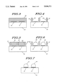
- FIG. 1 is a top plan view of an array of substrates with metalized pads.
- FIG. 2 is a top plan view of the array of substrates after application of solder paste.
- FIG. 3 is a cross-sectional view of a substrate covered with undefined solder resist.
- FIG. 4 is a cross sectional view of the substrate of FIG. 3 after selective delineation and removal of resist.
- FIG. 5 is a cross-sectional view of the substrate of FIG. 3 after application of solder paste.
- FIG. 6 is a cross-sectional view of the substrate of FIG. 3 after reflow of the paste.
- FIG. 7 is a cross-sectional view of the substrate of FIG. 3 after removal of the remaining resist.
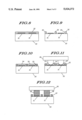
- FIG. 8 is a cross-sectional view of a substrate that can be used as a socket for a solder bumped member, shown covered with undefined solder resist.
- FIG. 9 is a cross-sectional view of the substrate of FIG. 8 after selective delineation and removal of resist.
- FIG. 10 is a cross-sectional view of the substrate of FIG. 8 after application of solder paste.
- FIG. 11 is a cross-sectional view of the substrate of FIG. 8 showing the positioned bumped member.
- FIG. 12 is a cross-sectional view of the substrate of FIG. 8 after reflow of the solder paste.
- a substrate 10 which includes fifteen pad grid arrays 11 on a single substrate.
- Each of the pad grid arrays 11 includes a plurality of metalized pads 12 arranged in a matrix.
- About the periphery of each pad grid array 11 is a plurality of side pads 13 and corner pads 14.
- the substrate 10 can be any desired material as for example ceramic.
- the individual pad grid arrays when separated can be used for electronic components such as for integrated circuit chip carriers.
- FIG. 2 illustrates the substrate 10 after the application of photo definable solder resist which has been exposed and processed to provide areas about the metalized pads 12, 13, and 14 which are slightly larger than the area of the metalized pads. These areas have been filled with solder paste 16 as is discussed below.
- FIG. 3 illustrates a substrate 20 which for clarity shows only two metalized pads 21 which can include a thin layer of solder.
- the substrate 20 can include any desired pattern of metalized pads 21, which can include a thin layer of solder.
- a thick layer of photo definable solder resist 22 is applied to the substrate 20.
- the resist 22 is preferably at least 10 mils. thick and preferably 15 mils. thick.
- Suitable photo definable solder resist is manufactured by Armstrong World Industries of Lancaster, Pa. and sold under the trademarks FANTON 106, 306, 370, or 363.
- the resist 22 is then exposed with ultraviolet radiation through a master stencil which defines the areas over the metalized pads 21 and can define an area larger than the metalized pads 21, by sensitizing the resist to then allow selective removal of the resist.
- solder paste 24 is then applied directly to the substrate 20 as by a squeegee.
- the remaining resist 22 acts essentially as a stencil capturing the solder paste 24 in the wells 23, as illustrated in FIG. 5.
- the size of the wells 23 is selected so that an appropriate amount of solder paste 24 is captured in each well.
- the solder paste 24 is then heated to reflow the solder and form the solder bumps 25 illustrated in FIG. 6.
- the height of the solder bumps 25 is determined by the composition of the solder paste 24, the area of the metalized pad 21, and by the dimensions of the well 23. Where higher solder bumps 25 are desired, larger wells 23 can be provided so that more solder paste 24 is available for reflow.
- a similar approach can be utilized for providing a mating substrate for attachment of a solder bumped substrate.
- a self-fixturing substrate is provided by substrate 30 of FIG. 8.
- the substrate 30 can be ceramic, polyimide, a printed circuit board or other substrate.
- the substrate 30 includes metalized pads 31 having a pattern corresponding to that of the solder bumped substrate to which it is being connected, such as that of FIG. 7.
- a photo definable solder resist 32 (which can be the same as resist 22) is applied over the substrate 30 and is delineated to define wells 33 in the photoresist 32, as illustrated in FIG. 9. Solder paste 34 is then directly applied, as by a squeegee, to fill the wells 33 as illustrated in FIG. 10.
- a solder bumped member 36 having solder bumps 37 which can be the solder bumped substrate 20 of FIG. 7, is positioned over the substrate 30 so that its solder bumps 37 settle into the solder paste 34.
- the wells 33 are preferably about 10 mils.
- solder bumps 37 tend to settle into the solder paste 34 under the force of gravity.
- the assembly is then heated to reflow the solder paste 34 for bonding with the solder bumps 37 and interconnecting the member 36 to substrate 30.
- a resulting solder interconnection is illustrated as solder 38 of FIG. 12.
- the solder paste 34 is selected to have a lower melting temperature than the solder of the solder bumps 37.
- the solder paste 34 will flow and wet to the metalized pads 31 and the solder bumps 37, blending with the solder bumps 37. While the solder bumps 37 can be reflowed, it is desirable not to reflow them in order avoid the possibility of the inadvertent shorting of adjacent solder bumps.
Abstract
Description
Claims (6)
Priority Applications (1)
| Application Number | Priority Date | Filing Date | Title |
|---|---|---|---|
| US07/520,995 US5024372A (en) | 1989-01-03 | 1990-05-09 | Method of making high density solder bumps and a substrate socket for high density solder bumps |
Applications Claiming Priority (2)
| Application Number | Priority Date | Filing Date | Title |
|---|---|---|---|
| US29298889A | 1989-01-03 | 1989-01-03 | |
| US07/520,995 US5024372A (en) | 1989-01-03 | 1990-05-09 | Method of making high density solder bumps and a substrate socket for high density solder bumps |
Related Parent Applications (1)
| Application Number | Title | Priority Date | Filing Date |
|---|---|---|---|
| US29298889A Continuation | 1989-01-03 | 1989-01-03 |
Publications (1)
| Publication Number | Publication Date |
|---|---|
| US5024372A true US5024372A (en) | 1991-06-18 |
Family
ID=26967676
Family Applications (1)
| Application Number | Title | Priority Date | Filing Date |
|---|---|---|---|
| US07/520,995 Expired - Fee Related US5024372A (en) | 1989-01-03 | 1990-05-09 | Method of making high density solder bumps and a substrate socket for high density solder bumps |
Country Status (1)
| Country | Link |
|---|---|
| US (1) | US5024372A (en) |
Cited By (117)
| Publication number | Priority date | Publication date | Assignee | Title |
|---|---|---|---|---|
| US5118027A (en) * | 1991-04-24 | 1992-06-02 | International Business Machines Corporation | Method of aligning and mounting solder balls to a substrate |
| US5162257A (en) * | 1991-09-13 | 1992-11-10 | Mcnc | Solder bump fabrication method |
| US5203075A (en) * | 1991-08-12 | 1993-04-20 | Inernational Business Machines | Method of bonding flexible circuit to cicuitized substrate to provide electrical connection therebetween using different solders |
| US5261155A (en) * | 1991-08-12 | 1993-11-16 | International Business Machines Corporation | Method for bonding flexible circuit to circuitized substrate to provide electrical connection therebetween using different solders |
| US5315070A (en) * | 1991-12-02 | 1994-05-24 | Siemens Aktiengesellschaft | Printed wiring board to which solder has been applied |
| EP0618757A1 (en) * | 1993-04-02 | 1994-10-05 | Siemens Aktiengesellschaft | Printed circuit board arrangement and process for producing printed circuit board |
| AU653945B2 (en) * | 1990-07-30 | 1994-10-20 | Industrial Development Corporation Of South Africa Limited | Attaching integrated circuits to circuit boards |
| DE4324479A1 (en) * | 1993-07-22 | 1995-03-09 | Blaupunkt Werke Gmbh | Method for producing structures which can be soldered in order to make contact with electrical modules |
| US5429293A (en) * | 1994-12-19 | 1995-07-04 | Motorola, Inc. | Soldering process |
| US5431332A (en) * | 1994-02-07 | 1995-07-11 | Motorola, Inc. | Method and apparatus for solder sphere placement using an air knife |
| US5452842A (en) * | 1993-05-03 | 1995-09-26 | Motorola, Inc. | Tin-zinc solder connection to a printed circuit board or the like |
| US5471011A (en) * | 1994-05-26 | 1995-11-28 | Ak Technology, Inc. | Homogeneous thermoplastic semi-conductor chip carrier package |
| US5482736A (en) * | 1994-08-04 | 1996-01-09 | Amkor Electronics, Inc. | Method for applying flux to ball grid array package |
| US5497545A (en) * | 1992-03-19 | 1996-03-12 | Hitachi, Ltd. | Method of making electrical connections in the manufacture of wiring sheet assemblies |
| US5499756A (en) * | 1995-02-03 | 1996-03-19 | Motorola, Inc. | Method of applying a tacking agent to a printed circuit board |
| US5531020A (en) * | 1989-11-14 | 1996-07-02 | Poly Flex Circuits, Inc. | Method of making subsurface electronic circuits |
| US5535936A (en) * | 1994-09-30 | 1996-07-16 | International Business Machines Corporation | Fine pitch solder formation on printed circuit board process and product |
| US5539153A (en) * | 1994-08-08 | 1996-07-23 | Hewlett-Packard Company | Method of bumping substrates by contained paste deposition |
| US5540379A (en) * | 1994-05-02 | 1996-07-30 | Motorola, Inc. | Soldering process |
| US5573171A (en) * | 1995-02-16 | 1996-11-12 | Trw Inc. | Method of thin film patterning by reflow |
| WO1997023903A1 (en) * | 1995-12-22 | 1997-07-03 | Tti Testron, Inc. | Method of placing contacts onto a substrate |
| US5658827A (en) * | 1994-11-09 | 1997-08-19 | International Business Machines Corporation | Method for forming solder balls on a substrate |
| WO1997040530A1 (en) * | 1996-04-19 | 1997-10-30 | Motorola Inc. | Solder bump apparatus, electronic component and method for forming a solder bump |
| US5735452A (en) * | 1996-06-17 | 1998-04-07 | International Business Machines Corporation | Ball grid array by partitioned lamination process |
| US5744759A (en) * | 1996-05-29 | 1998-04-28 | International Business Machines Corporation | Circuit boards that can accept a pluggable tab module that can be attached or removed without solder |
| US5759737A (en) * | 1996-09-06 | 1998-06-02 | International Business Machines Corporation | Method of making a component carrier |
| WO1998026318A1 (en) * | 1996-12-13 | 1998-06-18 | Commissariat A L'energie Atomique | Assembly of optical components optically aligned and method for making this assembly |
| US5787580A (en) * | 1996-11-19 | 1998-08-04 | Lg Information & Communications, Ltd. | Method for making radio-frequency module by ball grid array package |
| US5803340A (en) * | 1995-09-29 | 1998-09-08 | Delco Electronics Corporation | Composite solder paste for flip chip bumping |
| US5820014A (en) | 1993-11-16 | 1998-10-13 | Form Factor, Inc. | Solder preforms |
| US5872051A (en) * | 1995-08-02 | 1999-02-16 | International Business Machines Corporation | Process for transferring material to semiconductor chip conductive pads using a transfer substrate |
| US5874199A (en) * | 1995-11-30 | 1999-02-23 | International Business Machines Corporation | Method of forming oversized solder bumps |
| US5994152A (en) | 1996-02-21 | 1999-11-30 | Formfactor, Inc. | Fabricating interconnects and tips using sacrificial substrates |
| US6000603A (en) * | 1997-05-23 | 1999-12-14 | 3M Innovative Properties Company | Patterned array of metal balls and methods of making |
| US6024584A (en) * | 1996-10-10 | 2000-02-15 | Berg Technology, Inc. | High density connector |
| US6042389A (en) * | 1996-10-10 | 2000-03-28 | Berg Technology, Inc. | Low profile connector |
| US6053397A (en) * | 1996-11-12 | 2000-04-25 | Hewlett-Packard Company | Method for the manufacture of micro solder bumps on copper pads |
| US6077725A (en) * | 1992-09-03 | 2000-06-20 | Lucent Technologies Inc | Method for assembling multichip modules |
| US6085968A (en) * | 1999-01-22 | 2000-07-11 | Hewlett-Packard Company | Solder retention ring for improved solder bump formation |
| US6093035A (en) * | 1996-06-28 | 2000-07-25 | Berg Technology, Inc. | Contact for use in an electrical connector |
| US6137693A (en) * | 1998-07-31 | 2000-10-24 | Agilent Technologies Inc. | High-frequency electronic package with arbitrarily-shaped interconnects and integral shielding |
| US6139336A (en) * | 1996-11-14 | 2000-10-31 | Berg Technology, Inc. | High density connector having a ball type of contact surface |
| US6146203A (en) * | 1995-06-12 | 2000-11-14 | Berg Technology, Inc. | Low cross talk and impedance controlled electrical connector |
| US6156408A (en) * | 1997-08-29 | 2000-12-05 | Motorola, Inc. | Device for reworkable direct chip attachment |
| US6239385B1 (en) | 1998-02-27 | 2001-05-29 | Agilent Technologies, Inc. | Surface mountable coaxial solder interconnect and method |
| US6241535B1 (en) | 1996-10-10 | 2001-06-05 | Berg Technology, Inc. | Low profile connector |
| US6274823B1 (en) | 1993-11-16 | 2001-08-14 | Formfactor, Inc. | Interconnection substrates with resilient contact structures on both sides |
| US6287893B1 (en) | 1997-10-20 | 2001-09-11 | Flip Chip Technologies, L.L.C. | Method for forming chip scale package |
| US6293456B1 (en) | 1997-05-27 | 2001-09-25 | Spheretek, Llc | Methods for forming solder balls on substrates |
| US6316736B1 (en) | 1998-06-08 | 2001-11-13 | Visteon Global Technologies, Inc. | Anti-bridging solder ball collection zones |
| US6325644B1 (en) | 1996-10-10 | 2001-12-04 | Berg Technology, Inc. | High density connector and method of manufacture |
| US6329608B1 (en) | 1995-04-05 | 2001-12-11 | Unitive International Limited | Key-shaped solder bumps and under bump metallurgy |
| US20020014703A1 (en) * | 1997-07-21 | 2002-02-07 | Capote Miguel A. | Semiconductor flip-chip package and method for the fabrication thereof |
| US6388203B1 (en) | 1995-04-04 | 2002-05-14 | Unitive International Limited | Controlled-shaped solder reservoirs for increasing the volume of solder bumps, and structures formed thereby |
| US20020058356A1 (en) * | 1998-04-16 | 2002-05-16 | Yoichi Oya | Semiconductor package and mount board, and mounting method using the same |
| US6419148B1 (en) | 2001-01-23 | 2002-07-16 | Orbotech Ltd. | System for forming bumps on wafers |
| US6420255B1 (en) * | 1999-01-18 | 2002-07-16 | Nec Corporation | Mounting substrate with a solder resist layer and method of forming the same |
| US6547124B2 (en) * | 2001-06-14 | 2003-04-15 | Bae Systems Information And Electronic Systems Integration Inc. | Method for forming a micro column grid array (CGA) |
| US6609652B2 (en) | 1997-05-27 | 2003-08-26 | Spheretek, Llc | Ball bumping substrates, particuarly wafers |
| US20040026771A1 (en) * | 2001-09-10 | 2004-02-12 | Layman Paul Arthur | High-density inter-die interconnect structure |
| US6738600B1 (en) * | 2000-08-04 | 2004-05-18 | Harris Corporation | Ceramic microelectromechanical structure |
| US6759319B2 (en) | 2001-05-17 | 2004-07-06 | Institute Of Microelectronics | Residue-free solder bumping process |
| US20040175657A1 (en) * | 2003-03-06 | 2004-09-09 | International Business Machines Corporation | Dual-solder flip-chip solder bump |
| US20040209406A1 (en) * | 2003-02-18 | 2004-10-21 | Jong-Rong Jan | Methods of selectively bumping integrated circuit substrates and related structures |
| US20040209451A1 (en) * | 2003-04-15 | 2004-10-21 | Harima Chemicals, Inc. | Solder deposition method and solder bump forming method |
| US20040227592A1 (en) * | 2003-02-05 | 2004-11-18 | Chiu Luna H. | Method of applying patterned metallization to block filter resonators |
| US20040241906A1 (en) * | 2003-05-28 | 2004-12-02 | Vincent Chan | Integrated circuit package and method for making same that employs under bump metalization layer |
| US20050136641A1 (en) * | 2003-10-14 | 2005-06-23 | Rinne Glenn A. | Solder structures for out of plane connections and related methods |
| US20050140026A1 (en) * | 2001-09-07 | 2005-06-30 | Salmon Peter C. | Fabrication methods for electronic system modules |
| US20050150936A1 (en) * | 1997-05-27 | 2005-07-14 | Mackay John | Bumping electronic components using transfer substrates |
| US6939173B1 (en) | 1995-06-12 | 2005-09-06 | Fci Americas Technology, Inc. | Low cross talk and impedance controlled electrical connector with solder masses |
| US20050215045A1 (en) * | 2004-03-10 | 2005-09-29 | Rinne Glenn A | Methods of forming bumps using barrier layers as etch masks and related structures |
| US20050221675A1 (en) * | 2003-07-16 | 2005-10-06 | Rathburn James J | Fine pitch electrical interconnect assembly |
| US6960828B2 (en) | 2002-06-25 | 2005-11-01 | Unitive International Limited | Electronic structures including conductive shunt layers |
| EP1593450A1 (en) * | 2004-05-04 | 2005-11-09 | Agere System Inc. | Electronic device with surface mount components having stand-off space free of solder mask under the component - method for manfacturing the same |
| US20050279809A1 (en) * | 2000-11-10 | 2005-12-22 | Rinne Glenn A | Optical structures including liquid bumps and related methods |
| US20060035483A1 (en) * | 2003-07-16 | 2006-02-16 | Gryphics, Inc. | Fine pitch electrical interconnect assembly |
| US7007833B2 (en) | 1997-05-27 | 2006-03-07 | Mackay John | Forming solder balls on substrates |
| US20060076679A1 (en) * | 2002-06-25 | 2006-04-13 | Batchelor William E | Non-circular via holes for bumping pads and related structures |
| US20060125110A1 (en) * | 2004-12-09 | 2006-06-15 | Stats Chippac Ltd. | Method for solder bumping, and solder-bumping structures produced thereby |
| US20060205170A1 (en) * | 2005-03-09 | 2006-09-14 | Rinne Glenn A | Methods of forming self-healing metal-insulator-metal (MIM) structures and related devices |
| US7156284B2 (en) | 2000-12-15 | 2007-01-02 | Unitive International Limited | Low temperature methods of bonding components and related structures |
| US20070182004A1 (en) * | 2006-02-08 | 2007-08-09 | Rinne Glenn A | Methods of Forming Electronic Interconnections Including Compliant Dielectric Layers and Related Devices |
| US20070184604A1 (en) * | 1999-10-05 | 2007-08-09 | Nec Electronics Corporation | Multilayer interconnection board, semiconductor device having the same, and method of forming the same as well as method of mounting the semicondutor chip on the interconnection board |
| US20070245554A1 (en) * | 2001-09-07 | 2007-10-25 | Hynix Semiconductor, Inc. | Fabrication Method For Electronic System Modules |
| US7358174B2 (en) | 2004-04-13 | 2008-04-15 | Amkor Technology, Inc. | Methods of forming solder bumps on exposed metal pads |
| US20080087709A1 (en) * | 1997-05-27 | 2008-04-17 | Mackay John | Bumping Electronic Components Using Transfer Substrates |
| US20080182436A1 (en) * | 2003-07-16 | 2008-07-31 | Gryphics, Inc. | Fine pitch electrical interconnect assembly |
| US20080202804A1 (en) * | 2007-02-26 | 2008-08-28 | Yasuhiro Fakutomi | Printed circuit board and method of producing the same |
| US20090111259A1 (en) * | 2007-10-29 | 2009-04-30 | Applied Materials, Inc. | Methods for forming connective elements on integrated circuits for packaging applications |
| US7547623B2 (en) | 2002-06-25 | 2009-06-16 | Unitive International Limited | Methods of forming lead free solder bumps |
| US7654432B2 (en) | 1997-05-27 | 2010-02-02 | Wstp, Llc | Forming solder balls on substrates |
| US20100044416A1 (en) * | 2008-08-21 | 2010-02-25 | Nec Corporation | Method of manufacturing electronic components having bump |
| US7674701B2 (en) | 2006-02-08 | 2010-03-09 | Amkor Technology, Inc. | Methods of forming metal layers using multi-layer lift-off patterns |
| US20110092066A1 (en) * | 1997-05-27 | 2011-04-21 | Mackay John | Bumping Electronic Components Using Transfer Substrates |
| WO2011076788A1 (en) * | 2009-12-23 | 2011-06-30 | Pyreos Ltd. | Method for producing an infrared light detector |
| US8033838B2 (en) | 1996-02-21 | 2011-10-11 | Formfactor, Inc. | Microelectronic contact structure |
| US8044502B2 (en) | 2006-03-20 | 2011-10-25 | Gryphics, Inc. | Composite contact for fine pitch electrical interconnect assembly |
| US8373428B2 (en) | 1993-11-16 | 2013-02-12 | Formfactor, Inc. | Probe card assembly and kit, and methods of making same |
| USD718253S1 (en) | 2012-04-13 | 2014-11-25 | Fci Americas Technology Llc | Electrical cable connector |
| US8905651B2 (en) | 2012-01-31 | 2014-12-09 | Fci | Dismountable optical coupling device |
| USD720698S1 (en) | 2013-03-15 | 2015-01-06 | Fci Americas Technology Llc | Electrical cable connector |
| US8944831B2 (en) | 2012-04-13 | 2015-02-03 | Fci Americas Technology Llc | Electrical connector having ribbed ground plate with engagement members |
| US20150053752A1 (en) * | 2013-08-23 | 2015-02-26 | Chipmos Technologies Inc | Ball planting device and ball planting method thereof |
| USD727268S1 (en) | 2012-04-13 | 2015-04-21 | Fci Americas Technology Llc | Vertical electrical connector |
| USD727852S1 (en) | 2012-04-13 | 2015-04-28 | Fci Americas Technology Llc | Ground shield for a right angle electrical connector |
| US9048583B2 (en) | 2009-03-19 | 2015-06-02 | Fci Americas Technology Llc | Electrical connector having ribbed ground plate |
| USD733662S1 (en) | 2013-01-25 | 2015-07-07 | Fci Americas Technology Llc | Connector housing for electrical connector |
| USD746236S1 (en) | 2012-07-11 | 2015-12-29 | Fci Americas Technology Llc | Electrical connector housing |
| US9257778B2 (en) | 2012-04-13 | 2016-02-09 | Fci Americas Technology | High speed electrical connector |
| KR20160136305A (en) * | 2014-03-26 | 2016-11-29 | 소니 주식회사 | Semiconductor device, display panel, display device, electronic device, and method for manufacturing semiconductor device |
| US9543703B2 (en) | 2012-07-11 | 2017-01-10 | Fci Americas Technology Llc | Electrical connector with reduced stack height |
| US20170339785A1 (en) * | 2011-01-14 | 2017-11-23 | Harris Corporation | Method of making an electronic device having a liquid crystal polymer solder mask and related devices |
| WO2021050453A1 (en) * | 2019-09-12 | 2021-03-18 | Ormet Circuits, Inc. | Lithographically defined electrical interconnects from conductive pastes |
| DE102020129831A1 (en) | 2020-11-12 | 2022-05-12 | Endress+Hauser SE+Co. KG | Process for soldering a component onto a surface of a first printed circuit board |
| DE102020129830A1 (en) | 2020-11-12 | 2022-05-12 | Endress+Hauser SE+Co. KG | Method for soldering at least one first component onto a surface of a first printed circuit board |
| DE102021133746A1 (en) | 2021-12-17 | 2023-06-22 | Endress+Hauser SE+Co. KG | Process for soldering at least one component to at least one carrier element |
Citations (9)
| Publication number | Priority date | Publication date | Assignee | Title |
|---|---|---|---|---|
| US3436818A (en) * | 1965-12-13 | 1969-04-08 | Ibm | Method of fabricating a bonded joint |
| US3589000A (en) * | 1969-01-13 | 1971-06-29 | Du Pont | Method for attaching integrated circuit chips to thick film circuitry |
| US3986255A (en) * | 1974-11-29 | 1976-10-19 | Itek Corporation | Process for electrically interconnecting chips with substrates employing gold alloy bumps and magnetic materials therein |
| US4032058A (en) * | 1973-06-29 | 1977-06-28 | Ibm Corporation | Beam-lead integrated circuit structure and method for making the same including automatic registration of beam-leads with corresponding dielectric substrate leads |
| US4273859A (en) * | 1979-12-31 | 1981-06-16 | Honeywell Information Systems Inc. | Method of forming solder bump terminals on semiconductor elements |
| US4311267A (en) * | 1979-05-04 | 1982-01-19 | Gte Automatic Electric Laboratories, Inc. | Method of screening paste solder onto leaded hybrid substrates |
| JPS59136990A (en) * | 1983-01-26 | 1984-08-06 | オムロン株式会社 | Reflow soldering method |
| US4739917A (en) * | 1987-01-12 | 1988-04-26 | Ford Motor Company | Dual solder process for connecting electrically conducting terminals of electrical components to printed circuit conductors |
| US4818728A (en) * | 1986-12-03 | 1989-04-04 | Sharp Kabushiki Kaisha | Method of making a hybrid semiconductor device |
-
1990
- 1990-05-09 US US07/520,995 patent/US5024372A/en not_active Expired - Fee Related
Patent Citations (9)
| Publication number | Priority date | Publication date | Assignee | Title |
|---|---|---|---|---|
| US3436818A (en) * | 1965-12-13 | 1969-04-08 | Ibm | Method of fabricating a bonded joint |
| US3589000A (en) * | 1969-01-13 | 1971-06-29 | Du Pont | Method for attaching integrated circuit chips to thick film circuitry |
| US4032058A (en) * | 1973-06-29 | 1977-06-28 | Ibm Corporation | Beam-lead integrated circuit structure and method for making the same including automatic registration of beam-leads with corresponding dielectric substrate leads |
| US3986255A (en) * | 1974-11-29 | 1976-10-19 | Itek Corporation | Process for electrically interconnecting chips with substrates employing gold alloy bumps and magnetic materials therein |
| US4311267A (en) * | 1979-05-04 | 1982-01-19 | Gte Automatic Electric Laboratories, Inc. | Method of screening paste solder onto leaded hybrid substrates |
| US4273859A (en) * | 1979-12-31 | 1981-06-16 | Honeywell Information Systems Inc. | Method of forming solder bump terminals on semiconductor elements |
| JPS59136990A (en) * | 1983-01-26 | 1984-08-06 | オムロン株式会社 | Reflow soldering method |
| US4818728A (en) * | 1986-12-03 | 1989-04-04 | Sharp Kabushiki Kaisha | Method of making a hybrid semiconductor device |
| US4739917A (en) * | 1987-01-12 | 1988-04-26 | Ford Motor Company | Dual solder process for connecting electrically conducting terminals of electrical components to printed circuit conductors |
Non-Patent Citations (3)
| Title |
|---|
| IBM Technical Disclosure Bulletin, vol. 15, No. 5, p. 1715, Oct. 1972. * |
| IBM Technical Disclosure Bulletin, vol. 17, No. 8, p. 2331, Jan. 1975. * |
| Metals Handbook Ninth Edition, vol. 6, pp. 1100, 1101, copyright 1983. * |
Cited By (215)
| Publication number | Priority date | Publication date | Assignee | Title |
|---|---|---|---|---|
| US5531020A (en) * | 1989-11-14 | 1996-07-02 | Poly Flex Circuits, Inc. | Method of making subsurface electronic circuits |
| AU653945B2 (en) * | 1990-07-30 | 1994-10-20 | Industrial Development Corporation Of South Africa Limited | Attaching integrated circuits to circuit boards |
| US5118027A (en) * | 1991-04-24 | 1992-06-02 | International Business Machines Corporation | Method of aligning and mounting solder balls to a substrate |
| US5203075A (en) * | 1991-08-12 | 1993-04-20 | Inernational Business Machines | Method of bonding flexible circuit to cicuitized substrate to provide electrical connection therebetween using different solders |
| US5261155A (en) * | 1991-08-12 | 1993-11-16 | International Business Machines Corporation | Method for bonding flexible circuit to circuitized substrate to provide electrical connection therebetween using different solders |
| US5162257A (en) * | 1991-09-13 | 1992-11-10 | Mcnc | Solder bump fabrication method |
| US5293006A (en) * | 1991-09-13 | 1994-03-08 | Mcnc | Solder bump including circular lip |
| US5315070A (en) * | 1991-12-02 | 1994-05-24 | Siemens Aktiengesellschaft | Printed wiring board to which solder has been applied |
| US5497545A (en) * | 1992-03-19 | 1996-03-12 | Hitachi, Ltd. | Method of making electrical connections in the manufacture of wiring sheet assemblies |
| US6077725A (en) * | 1992-09-03 | 2000-06-20 | Lucent Technologies Inc | Method for assembling multichip modules |
| EP0618757A1 (en) * | 1993-04-02 | 1994-10-05 | Siemens Aktiengesellschaft | Printed circuit board arrangement and process for producing printed circuit board |
| US5452842A (en) * | 1993-05-03 | 1995-09-26 | Motorola, Inc. | Tin-zinc solder connection to a printed circuit board or the like |
| DE4324479A1 (en) * | 1993-07-22 | 1995-03-09 | Blaupunkt Werke Gmbh | Method for producing structures which can be soldered in order to make contact with electrical modules |
| DE4324479B4 (en) * | 1993-07-22 | 2009-03-26 | Robert Bosch Gmbh | Process for producing solderable structures for contacting electrical modules |
| US6274823B1 (en) | 1993-11-16 | 2001-08-14 | Formfactor, Inc. | Interconnection substrates with resilient contact structures on both sides |
| US5820014A (en) | 1993-11-16 | 1998-10-13 | Form Factor, Inc. | Solder preforms |
| US8373428B2 (en) | 1993-11-16 | 2013-02-12 | Formfactor, Inc. | Probe card assembly and kit, and methods of making same |
| US5431332A (en) * | 1994-02-07 | 1995-07-11 | Motorola, Inc. | Method and apparatus for solder sphere placement using an air knife |
| US5540379A (en) * | 1994-05-02 | 1996-07-30 | Motorola, Inc. | Soldering process |
| US5471011A (en) * | 1994-05-26 | 1995-11-28 | Ak Technology, Inc. | Homogeneous thermoplastic semi-conductor chip carrier package |
| US5482736A (en) * | 1994-08-04 | 1996-01-09 | Amkor Electronics, Inc. | Method for applying flux to ball grid array package |
| US5539153A (en) * | 1994-08-08 | 1996-07-23 | Hewlett-Packard Company | Method of bumping substrates by contained paste deposition |
| US5586715A (en) * | 1994-08-08 | 1996-12-24 | Hewlett-Packard Company | Method of making solder balls by contained paste deposition |
| EP0697727A3 (en) * | 1994-08-08 | 1997-04-09 | Hewlett Packard Co | Method of bumping substrates |
| US5672542A (en) * | 1994-08-08 | 1997-09-30 | Hewlett Packard Company | Method of making solder balls by contained paste deposition |
| US6030889A (en) * | 1994-09-11 | 2000-02-29 | International Business Machines Corporation | Substrate-holding fixture of non-wettable material |
| US5535936A (en) * | 1994-09-30 | 1996-07-16 | International Business Machines Corporation | Fine pitch solder formation on printed circuit board process and product |
| US5658827A (en) * | 1994-11-09 | 1997-08-19 | International Business Machines Corporation | Method for forming solder balls on a substrate |
| US5429293A (en) * | 1994-12-19 | 1995-07-04 | Motorola, Inc. | Soldering process |
| WO1996019913A1 (en) * | 1994-12-19 | 1996-06-27 | Motorola Inc. | Soldering process |
| US5499756A (en) * | 1995-02-03 | 1996-03-19 | Motorola, Inc. | Method of applying a tacking agent to a printed circuit board |
| US5573171A (en) * | 1995-02-16 | 1996-11-12 | Trw Inc. | Method of thin film patterning by reflow |
| US6388203B1 (en) | 1995-04-04 | 2002-05-14 | Unitive International Limited | Controlled-shaped solder reservoirs for increasing the volume of solder bumps, and structures formed thereby |
| US6392163B1 (en) | 1995-04-04 | 2002-05-21 | Unitive International Limited | Controlled-shaped solder reservoirs for increasing the volume of solder bumps |
| US6389691B1 (en) * | 1995-04-05 | 2002-05-21 | Unitive International Limited | Methods for forming integrated redistribution routing conductors and solder bumps |
| US6329608B1 (en) | 1995-04-05 | 2001-12-11 | Unitive International Limited | Key-shaped solder bumps and under bump metallurgy |
| US6146203A (en) * | 1995-06-12 | 2000-11-14 | Berg Technology, Inc. | Low cross talk and impedance controlled electrical connector |
| US6939173B1 (en) | 1995-06-12 | 2005-09-06 | Fci Americas Technology, Inc. | Low cross talk and impedance controlled electrical connector with solder masses |
| US5872051A (en) * | 1995-08-02 | 1999-02-16 | International Business Machines Corporation | Process for transferring material to semiconductor chip conductive pads using a transfer substrate |
| US5803340A (en) * | 1995-09-29 | 1998-09-08 | Delco Electronics Corporation | Composite solder paste for flip chip bumping |
| US5874199A (en) * | 1995-11-30 | 1999-02-23 | International Business Machines Corporation | Method of forming oversized solder bumps |
| US5782399A (en) * | 1995-12-22 | 1998-07-21 | Tti Testron, Inc. | Method and apparatus for attaching spherical and/or non-spherical contacts to a substrate |
| WO1997023903A1 (en) * | 1995-12-22 | 1997-07-03 | Tti Testron, Inc. | Method of placing contacts onto a substrate |
| US6112975A (en) * | 1995-12-22 | 2000-09-05 | Delaware Capital Formation, Inc. | Method for attaching spherical and/or non-spherical contacts to a substrate |
| US5994152A (en) | 1996-02-21 | 1999-11-30 | Formfactor, Inc. | Fabricating interconnects and tips using sacrificial substrates |
| US8033838B2 (en) | 1996-02-21 | 2011-10-11 | Formfactor, Inc. | Microelectronic contact structure |
| WO1997040530A1 (en) * | 1996-04-19 | 1997-10-30 | Motorola Inc. | Solder bump apparatus, electronic component and method for forming a solder bump |
| US5738269A (en) * | 1996-04-19 | 1998-04-14 | Motorola, Inc. | Method for forming a solder bump |
| US6070785A (en) * | 1996-05-29 | 2000-06-06 | International Business Machines Corporation | Process for manufacturing boards that can accept a pluggable tab module that can be attached or removed without solder |
| US5744759A (en) * | 1996-05-29 | 1998-04-28 | International Business Machines Corporation | Circuit boards that can accept a pluggable tab module that can be attached or removed without solder |
| US5735452A (en) * | 1996-06-17 | 1998-04-07 | International Business Machines Corporation | Ball grid array by partitioned lamination process |
| US6093035A (en) * | 1996-06-28 | 2000-07-25 | Berg Technology, Inc. | Contact for use in an electrical connector |
| US5759737A (en) * | 1996-09-06 | 1998-06-02 | International Business Machines Corporation | Method of making a component carrier |
| US8167630B2 (en) | 1996-10-10 | 2012-05-01 | Fci Americas Technology Llc | High density connector and method of manufacture |
| US6042389A (en) * | 1996-10-10 | 2000-03-28 | Berg Technology, Inc. | Low profile connector |
| US6079991A (en) * | 1996-10-10 | 2000-06-27 | Berg Technology, Inc. | Method for placing contact on electrical connector |
| US6164983A (en) * | 1996-10-10 | 2000-12-26 | Berg Technology, Inc. | High density connector |
| US6358068B1 (en) | 1996-10-10 | 2002-03-19 | Fci Americas Technology, Inc. | Stress resistant connector and method for reducing stress in housing thereof |
| US6241535B1 (en) | 1996-10-10 | 2001-06-05 | Berg Technology, Inc. | Low profile connector |
| US6024584A (en) * | 1996-10-10 | 2000-02-15 | Berg Technology, Inc. | High density connector |
| US7186123B2 (en) | 1996-10-10 | 2007-03-06 | Fci Americas Technology, Inc. | High density connector and method of manufacture |
| US6325644B1 (en) | 1996-10-10 | 2001-12-04 | Berg Technology, Inc. | High density connector and method of manufacture |
| US6053397A (en) * | 1996-11-12 | 2000-04-25 | Hewlett-Packard Company | Method for the manufacture of micro solder bumps on copper pads |
| US6247635B1 (en) | 1996-11-14 | 2001-06-19 | Berg Technology, Inc. | High density connector having a ball type of contact surface |
| US6139336A (en) * | 1996-11-14 | 2000-10-31 | Berg Technology, Inc. | High density connector having a ball type of contact surface |
| US5787580A (en) * | 1996-11-19 | 1998-08-04 | Lg Information & Communications, Ltd. | Method for making radio-frequency module by ball grid array package |
| FR2757276A1 (en) * | 1996-12-13 | 1998-06-19 | Commissariat Energie Atomique | ASSEMBLY OF OPTICALLY ALIGNED OPTICAL COMPONENTS AND METHOD FOR MANUFACTURING THE ASSEMBLY |
| WO1998026318A1 (en) * | 1996-12-13 | 1998-06-18 | Commissariat A L'energie Atomique | Assembly of optical components optically aligned and method for making this assembly |
| US6000603A (en) * | 1997-05-23 | 1999-12-14 | 3M Innovative Properties Company | Patterned array of metal balls and methods of making |
| US7604153B2 (en) | 1997-05-27 | 2009-10-20 | Wstp, Llc | Forming solder balls on substrates |
| US20080087709A1 (en) * | 1997-05-27 | 2008-04-17 | Mackay John | Bumping Electronic Components Using Transfer Substrates |
| US7819301B2 (en) | 1997-05-27 | 2010-10-26 | Wstp, Llc | Bumping electronic components using transfer substrates |
| US20110092066A1 (en) * | 1997-05-27 | 2011-04-21 | Mackay John | Bumping Electronic Components Using Transfer Substrates |
| US6293456B1 (en) | 1997-05-27 | 2001-09-25 | Spheretek, Llc | Methods for forming solder balls on substrates |
| US20050150936A1 (en) * | 1997-05-27 | 2005-07-14 | Mackay John | Bumping electronic components using transfer substrates |
| US20060208041A1 (en) * | 1997-05-27 | 2006-09-21 | Mackay John | Forming solder balls on substrates |
| US6609652B2 (en) | 1997-05-27 | 2003-08-26 | Spheretek, Llc | Ball bumping substrates, particuarly wafers |
| US7288471B2 (en) | 1997-05-27 | 2007-10-30 | Mackay John | Bumping electronic components using transfer substrates |
| US7007833B2 (en) | 1997-05-27 | 2006-03-07 | Mackay John | Forming solder balls on substrates |
| US7654432B2 (en) | 1997-05-27 | 2010-02-02 | Wstp, Llc | Forming solder balls on substrates |
| US20020014703A1 (en) * | 1997-07-21 | 2002-02-07 | Capote Miguel A. | Semiconductor flip-chip package and method for the fabrication thereof |
| US6156408A (en) * | 1997-08-29 | 2000-12-05 | Motorola, Inc. | Device for reworkable direct chip attachment |
| US6441487B2 (en) | 1997-10-20 | 2002-08-27 | Flip Chip Technologies, L.L.C. | Chip scale package using large ductile solder balls |
| US6287893B1 (en) | 1997-10-20 | 2001-09-11 | Flip Chip Technologies, L.L.C. | Method for forming chip scale package |
| US6750135B2 (en) | 1997-10-20 | 2004-06-15 | Flip Chip Technologies, L.L.C. | Method for forming chip scale package |
| US6239385B1 (en) | 1998-02-27 | 2001-05-29 | Agilent Technologies, Inc. | Surface mountable coaxial solder interconnect and method |
| US20020058356A1 (en) * | 1998-04-16 | 2002-05-16 | Yoichi Oya | Semiconductor package and mount board, and mounting method using the same |
| US6316736B1 (en) | 1998-06-08 | 2001-11-13 | Visteon Global Technologies, Inc. | Anti-bridging solder ball collection zones |
| US6137693A (en) * | 1998-07-31 | 2000-10-24 | Agilent Technologies Inc. | High-frequency electronic package with arbitrarily-shaped interconnects and integral shielding |
| US6420255B1 (en) * | 1999-01-18 | 2002-07-16 | Nec Corporation | Mounting substrate with a solder resist layer and method of forming the same |
| US6085968A (en) * | 1999-01-22 | 2000-07-11 | Hewlett-Packard Company | Solder retention ring for improved solder bump formation |
| US20070184604A1 (en) * | 1999-10-05 | 2007-08-09 | Nec Electronics Corporation | Multilayer interconnection board, semiconductor device having the same, and method of forming the same as well as method of mounting the semicondutor chip on the interconnection board |
| US8008130B2 (en) * | 1999-10-05 | 2011-08-30 | Renesas Electronics Corporation | Multilayer interconnection board, semiconductor device having the same, and method of forming the same as well as method of mounting the semicondutor chip on the interconnection board |
| US6738600B1 (en) * | 2000-08-04 | 2004-05-18 | Harris Corporation | Ceramic microelectromechanical structure |
| US20040198231A1 (en) * | 2000-08-04 | 2004-10-07 | Harris Corporation | Ceramic microelectromechanical structure |
| US7035591B2 (en) | 2000-08-04 | 2006-04-25 | Harris Corporation | Ceramic microelectromechanical structure |
| US7213740B2 (en) | 2000-11-10 | 2007-05-08 | Unitive International Limited | Optical structures including liquid bumps and related methods |
| US20050279809A1 (en) * | 2000-11-10 | 2005-12-22 | Rinne Glenn A | Optical structures including liquid bumps and related methods |
| US20070152020A1 (en) * | 2000-11-10 | 2007-07-05 | Unitive International Limited | Optical structures including liquid bumps |
| US7156284B2 (en) | 2000-12-15 | 2007-01-02 | Unitive International Limited | Low temperature methods of bonding components and related structures |
| US6419148B1 (en) | 2001-01-23 | 2002-07-16 | Orbotech Ltd. | System for forming bumps on wafers |
| US6759319B2 (en) | 2001-05-17 | 2004-07-06 | Institute Of Microelectronics | Residue-free solder bumping process |
| US6547124B2 (en) * | 2001-06-14 | 2003-04-15 | Bae Systems Information And Electronic Systems Integration Inc. | Method for forming a micro column grid array (CGA) |
| US8252635B2 (en) | 2001-09-07 | 2012-08-28 | Hynix Semiconductor Inc. | Electronic system modules and method of fabrication |
| US8581407B2 (en) | 2001-09-07 | 2013-11-12 | SK Hynix Inc. | Electronic system modules and method of fabrication |
| US20100007012A1 (en) * | 2001-09-07 | 2010-01-14 | Hynix Semiconductor Inc. | Electronic system modules |
| US20090243076A1 (en) * | 2001-09-07 | 2009-10-01 | Hynix Semiconductor, Inc. | Electronic system modules and method of fabrication |
| US20070245554A1 (en) * | 2001-09-07 | 2007-10-25 | Hynix Semiconductor, Inc. | Fabrication Method For Electronic System Modules |
| US9059070B2 (en) | 2001-09-07 | 2015-06-16 | SK Hynix Inc. | Electronic system modules and method of fabrication |
| US7723156B2 (en) | 2001-09-07 | 2010-05-25 | Hynix Semiconductor Inc. | Electronic system modules and method of fabrication |
| US20100297814A1 (en) * | 2001-09-07 | 2010-11-25 | Hynix Semiconductor Inc. | Electronic system modules and method of fabrication |
| US20050140026A1 (en) * | 2001-09-07 | 2005-06-30 | Salmon Peter C. | Fabrication methods for electronic system modules |
| US20080026557A1 (en) * | 2001-09-07 | 2008-01-31 | Hynix Semiconductor, Inc. | Electronic system modules and method of fabrication |
| US7615478B2 (en) | 2001-09-07 | 2009-11-10 | Hynix Semiconductor Inc. | Fabrication method for electronic system modules |
| US8633584B2 (en) | 2001-09-07 | 2014-01-21 | SK Hynix Inc. | Electronic assembly with electronic compontent and interconnection assembly connected via conductive bump and mating well |
| US20080079140A1 (en) * | 2001-09-07 | 2008-04-03 | Hynix Semiconductor, Inc. | Electronic system modules and method of fabricaton |
| US7045835B2 (en) | 2001-09-10 | 2006-05-16 | Agere Systems Inc. | High-density inter-die interconnect structure |
| US20060166395A1 (en) * | 2001-09-10 | 2006-07-27 | Layman Paul A | High-density inter-die interconnect structure |
| US20040026771A1 (en) * | 2001-09-10 | 2004-02-12 | Layman Paul Arthur | High-density inter-die interconnect structure |
| US20110084392A1 (en) * | 2002-06-25 | 2011-04-14 | Nair Krishna K | Electronic Structures Including Conductive Layers Comprising Copper and Having a Thickness of at Least 0.5 Micrometers |
| US20090212427A1 (en) * | 2002-06-25 | 2009-08-27 | Unitive International Limited | Solder Structures Including Barrier Layers with Nickel and/or Copper |
| US20080026560A1 (en) * | 2002-06-25 | 2008-01-31 | Unitive International Limited | Methods of forming electronic structures including conductive shunt layers and related structures |
| US7297631B2 (en) | 2002-06-25 | 2007-11-20 | Unitive International Limited | Methods of forming electronic structures including conductive shunt layers and related structures |
| US20060076679A1 (en) * | 2002-06-25 | 2006-04-13 | Batchelor William E | Non-circular via holes for bumping pads and related structures |
| US20060009023A1 (en) * | 2002-06-25 | 2006-01-12 | Unitive International Limited | Methods of forming electronic structures including conductive shunt layers and related structures |
| US7839000B2 (en) | 2002-06-25 | 2010-11-23 | Unitive International Limited | Solder structures including barrier layers with nickel and/or copper |
| US7531898B2 (en) | 2002-06-25 | 2009-05-12 | Unitive International Limited | Non-Circular via holes for bumping pads and related structures |
| US7879715B2 (en) | 2002-06-25 | 2011-02-01 | Unitive International Limited | Methods of forming electronic structures including conductive shunt layers and related structures |
| US7547623B2 (en) | 2002-06-25 | 2009-06-16 | Unitive International Limited | Methods of forming lead free solder bumps |
| US6960828B2 (en) | 2002-06-25 | 2005-11-01 | Unitive International Limited | Electronic structures including conductive shunt layers |
| US8294269B2 (en) | 2002-06-25 | 2012-10-23 | Unitive International | Electronic structures including conductive layers comprising copper and having a thickness of at least 0.5 micrometers |
| US20040227592A1 (en) * | 2003-02-05 | 2004-11-18 | Chiu Luna H. | Method of applying patterned metallization to block filter resonators |
| US7081404B2 (en) | 2003-02-18 | 2006-07-25 | Unitive Electronics Inc. | Methods of selectively bumping integrated circuit substrates and related structures |
| US7579694B2 (en) | 2003-02-18 | 2009-08-25 | Unitive International Limited | Electronic devices including offset conductive bumps |
| US20060231951A1 (en) * | 2003-02-18 | 2006-10-19 | Jong-Rong Jan | Electronic devices including offset conductive bumps |
| US20040209406A1 (en) * | 2003-02-18 | 2004-10-21 | Jong-Rong Jan | Methods of selectively bumping integrated circuit substrates and related structures |
| US6893799B2 (en) | 2003-03-06 | 2005-05-17 | International Business Machines Corporation | Dual-solder flip-chip solder bump |
| US20040175657A1 (en) * | 2003-03-06 | 2004-09-09 | International Business Machines Corporation | Dual-solder flip-chip solder bump |
| US7452797B2 (en) * | 2003-04-15 | 2008-11-18 | Harima Chemicals, Inc. | Solder deposition method and solder bump forming method |
| US20040209451A1 (en) * | 2003-04-15 | 2004-10-21 | Harima Chemicals, Inc. | Solder deposition method and solder bump forming method |
| US20040241906A1 (en) * | 2003-05-28 | 2004-12-02 | Vincent Chan | Integrated circuit package and method for making same that employs under bump metalization layer |
| US20050221675A1 (en) * | 2003-07-16 | 2005-10-06 | Rathburn James J | Fine pitch electrical interconnect assembly |
| US7297003B2 (en) | 2003-07-16 | 2007-11-20 | Gryphics, Inc. | Fine pitch electrical interconnect assembly |
| US7537461B2 (en) | 2003-07-16 | 2009-05-26 | Gryphics, Inc. | Fine pitch electrical interconnect assembly |
| US20060035483A1 (en) * | 2003-07-16 | 2006-02-16 | Gryphics, Inc. | Fine pitch electrical interconnect assembly |
| US7422439B2 (en) | 2003-07-16 | 2008-09-09 | Gryphics, Inc. | Fine pitch electrical interconnect assembly |
| US20080182436A1 (en) * | 2003-07-16 | 2008-07-31 | Gryphics, Inc. | Fine pitch electrical interconnect assembly |
| US20080057753A1 (en) * | 2003-07-16 | 2008-03-06 | Gryphics, Inc | Fine pitch electrical interconnect assembly |
| US7326064B2 (en) | 2003-07-16 | 2008-02-05 | Gryphics, Inc. | Fine pitch electrical interconnect assembly |
| US20050136641A1 (en) * | 2003-10-14 | 2005-06-23 | Rinne Glenn A. | Solder structures for out of plane connections and related methods |
| US20060138675A1 (en) * | 2003-10-14 | 2006-06-29 | Rinne Glenn A | Solder structures for out of plane connections |
| US7049216B2 (en) | 2003-10-14 | 2006-05-23 | Unitive International Limited | Methods of providing solder structures for out plane connections |
| US7659621B2 (en) | 2003-10-14 | 2010-02-09 | Unitive International Limited | Solder structures for out of plane connections |
| US20080308931A1 (en) * | 2004-03-10 | 2008-12-18 | Unitive International Limited | Electronic Structures Including Barrier Layers Defining Lips |
| US7834454B2 (en) | 2004-03-10 | 2010-11-16 | Unitive International Limited | Electronic structures including barrier layers defining lips |
| US20050215045A1 (en) * | 2004-03-10 | 2005-09-29 | Rinne Glenn A | Methods of forming bumps using barrier layers as etch masks and related structures |
| US8487432B2 (en) | 2004-03-10 | 2013-07-16 | Amkor Technology, Inc. | Electronic structures including barrier layers and/or oxidation barriers defining lips and related methods |
| US7427557B2 (en) | 2004-03-10 | 2008-09-23 | Unitive International Limited | Methods of forming bumps using barrier layers as etch masks |
| US20110037171A1 (en) * | 2004-03-10 | 2011-02-17 | Rinne Glenn A | Electronic Structures Including Barrier Layers and/or Oxidation Barriers Defining Lips and Related Methods |
| US7358174B2 (en) | 2004-04-13 | 2008-04-15 | Amkor Technology, Inc. | Methods of forming solder bumps on exposed metal pads |
| EP1593450A1 (en) * | 2004-05-04 | 2005-11-09 | Agere System Inc. | Electronic device with surface mount components having stand-off space free of solder mask under the component - method for manfacturing the same |
| US20080041620A1 (en) * | 2004-05-04 | 2008-02-21 | Albanese Patricia M | Surface mount attachment of components |
| US20060125110A1 (en) * | 2004-12-09 | 2006-06-15 | Stats Chippac Ltd. | Method for solder bumping, and solder-bumping structures produced thereby |
| US7410824B2 (en) | 2004-12-09 | 2008-08-12 | Stats Chippac Ltd. | Method for solder bumping, and solder-bumping structures produced thereby |
| US20080230925A1 (en) * | 2004-12-09 | 2008-09-25 | Byung Tai Do | Solder-bumping structures produced by a solder bumping method |
| US20060205170A1 (en) * | 2005-03-09 | 2006-09-14 | Rinne Glenn A | Methods of forming self-healing metal-insulator-metal (MIM) structures and related devices |
| US7932615B2 (en) | 2006-02-08 | 2011-04-26 | Amkor Technology, Inc. | Electronic devices including solder bumps on compliant dielectric layers |
| US20070182004A1 (en) * | 2006-02-08 | 2007-08-09 | Rinne Glenn A | Methods of Forming Electronic Interconnections Including Compliant Dielectric Layers and Related Devices |
| US7674701B2 (en) | 2006-02-08 | 2010-03-09 | Amkor Technology, Inc. | Methods of forming metal layers using multi-layer lift-off patterns |
| US8232632B2 (en) | 2006-03-20 | 2012-07-31 | R&D Sockets, Inc. | Composite contact for fine pitch electrical interconnect assembly |
| US8044502B2 (en) | 2006-03-20 | 2011-10-25 | Gryphics, Inc. | Composite contact for fine pitch electrical interconnect assembly |
| US20080202804A1 (en) * | 2007-02-26 | 2008-08-28 | Yasuhiro Fakutomi | Printed circuit board and method of producing the same |
| US20090111259A1 (en) * | 2007-10-29 | 2009-04-30 | Applied Materials, Inc. | Methods for forming connective elements on integrated circuits for packaging applications |
| US7767586B2 (en) * | 2007-10-29 | 2010-08-03 | Applied Materials, Inc. | Methods for forming connective elements on integrated circuits for packaging applications |
| US20100044416A1 (en) * | 2008-08-21 | 2010-02-25 | Nec Corporation | Method of manufacturing electronic components having bump |
| US10720721B2 (en) | 2009-03-19 | 2020-07-21 | Fci Usa Llc | Electrical connector having ribbed ground plate |
| US10096921B2 (en) | 2009-03-19 | 2018-10-09 | Fci Usa Llc | Electrical connector having ribbed ground plate |
| US9461410B2 (en) | 2009-03-19 | 2016-10-04 | Fci Americas Technology Llc | Electrical connector having ribbed ground plate |
| US9048583B2 (en) | 2009-03-19 | 2015-06-02 | Fci Americas Technology Llc | Electrical connector having ribbed ground plate |
| WO2011076788A1 (en) * | 2009-12-23 | 2011-06-30 | Pyreos Ltd. | Method for producing an infrared light detector |
| US8987035B2 (en) | 2009-12-23 | 2015-03-24 | Pyreos, Ltd. | Method for producing an infrared light detector |
| CN102763221A (en) * | 2009-12-23 | 2012-10-31 | 派洛斯有限公司 | Method for producing an infrared light detector |
| CN102763221B (en) * | 2009-12-23 | 2015-06-10 | 派洛斯有限公司 | Method for producing an infrared light detector |
| US10342126B2 (en) * | 2011-01-14 | 2019-07-02 | Harris Corporation | Electronic device having a liquid crystal polymer solder mask and related devices |
| US20170339785A1 (en) * | 2011-01-14 | 2017-11-23 | Harris Corporation | Method of making an electronic device having a liquid crystal polymer solder mask and related devices |
| US8905651B2 (en) | 2012-01-31 | 2014-12-09 | Fci | Dismountable optical coupling device |
| USD727268S1 (en) | 2012-04-13 | 2015-04-21 | Fci Americas Technology Llc | Vertical electrical connector |
| USD790471S1 (en) | 2012-04-13 | 2017-06-27 | Fci Americas Technology Llc | Vertical electrical connector |
| USD718253S1 (en) | 2012-04-13 | 2014-11-25 | Fci Americas Technology Llc | Electrical cable connector |
| US8944831B2 (en) | 2012-04-13 | 2015-02-03 | Fci Americas Technology Llc | Electrical connector having ribbed ground plate with engagement members |
| USD748063S1 (en) | 2012-04-13 | 2016-01-26 | Fci Americas Technology Llc | Electrical ground shield |
| US9257778B2 (en) | 2012-04-13 | 2016-02-09 | Fci Americas Technology | High speed electrical connector |
| USD750030S1 (en) | 2012-04-13 | 2016-02-23 | Fci Americas Technology Llc | Electrical cable connector |
| USD750025S1 (en) | 2012-04-13 | 2016-02-23 | Fci Americas Technology Llc | Vertical electrical connector |
| USD816044S1 (en) | 2012-04-13 | 2018-04-24 | Fci Americas Technology Llc | Electrical cable connector |
| US9831605B2 (en) | 2012-04-13 | 2017-11-28 | Fci Americas Technology Llc | High speed electrical connector |
| USD727852S1 (en) | 2012-04-13 | 2015-04-28 | Fci Americas Technology Llc | Ground shield for a right angle electrical connector |
| USD751507S1 (en) | 2012-07-11 | 2016-03-15 | Fci Americas Technology Llc | Electrical connector |
| US9871323B2 (en) | 2012-07-11 | 2018-01-16 | Fci Americas Technology Llc | Electrical connector with reduced stack height |
| US9543703B2 (en) | 2012-07-11 | 2017-01-10 | Fci Americas Technology Llc | Electrical connector with reduced stack height |
| USD746236S1 (en) | 2012-07-11 | 2015-12-29 | Fci Americas Technology Llc | Electrical connector housing |
| USD745852S1 (en) | 2013-01-25 | 2015-12-22 | Fci Americas Technology Llc | Electrical connector |
| USD766832S1 (en) | 2013-01-25 | 2016-09-20 | Fci Americas Technology Llc | Electrical connector |
| USD772168S1 (en) | 2013-01-25 | 2016-11-22 | Fci Americas Technology Llc | Connector housing for electrical connector |
| USD733662S1 (en) | 2013-01-25 | 2015-07-07 | Fci Americas Technology Llc | Connector housing for electrical connector |
| USD720698S1 (en) | 2013-03-15 | 2015-01-06 | Fci Americas Technology Llc | Electrical cable connector |
| US20150053752A1 (en) * | 2013-08-23 | 2015-02-26 | Chipmos Technologies Inc | Ball planting device and ball planting method thereof |
| US10304787B2 (en) * | 2014-03-26 | 2019-05-28 | Sony Semiconductor Solutions Corporation | Semiconductor device, display panel, display device, and electronic device |
| CN106937533A (en) * | 2014-03-26 | 2017-07-07 | 索尼公司 | The method of semiconductor device, display panel, display device, electronic installation and manufacture semiconductor device |
| US20170117262A1 (en) * | 2014-03-26 | 2017-04-27 | Sony Corporation | Semiconductor device, display panel, display device, electronic device, and method of manufacturing semiconductor device |
| KR20160136305A (en) * | 2014-03-26 | 2016-11-29 | 소니 주식회사 | Semiconductor device, display panel, display device, electronic device, and method for manufacturing semiconductor device |
| WO2021050453A1 (en) * | 2019-09-12 | 2021-03-18 | Ormet Circuits, Inc. | Lithographically defined electrical interconnects from conductive pastes |
| DE102020129831A1 (en) | 2020-11-12 | 2022-05-12 | Endress+Hauser SE+Co. KG | Process for soldering a component onto a surface of a first printed circuit board |
| DE102020129830A1 (en) | 2020-11-12 | 2022-05-12 | Endress+Hauser SE+Co. KG | Method for soldering at least one first component onto a surface of a first printed circuit board |
| DE102021133746A1 (en) | 2021-12-17 | 2023-06-22 | Endress+Hauser SE+Co. KG | Process for soldering at least one component to at least one carrier element |
Similar Documents
| Publication | Publication Date | Title |
|---|---|---|
| US5024372A (en) | Method of making high density solder bumps and a substrate socket for high density solder bumps | |
| CA2135508C (en) | Method for forming solder balls on a semiconductor substrate | |
| US6454159B1 (en) | Method for forming electrical connecting structure | |
| US5641113A (en) | Method for fabricating an electronic device having solder joints | |
| US9545014B2 (en) | Flip chip interconnect solder mask | |
| EP0403631B1 (en) | Method of making high density solder bumps and a substrate socket for high density solder bumps | |
| JP2596721B2 (en) | Method of manufacturing integrated circuit chip for DCA | |
| US5482736A (en) | Method for applying flux to ball grid array package | |
| US5860585A (en) | Substrate for transferring bumps and method of use | |
| US6127204A (en) | Column grid array or ball grid array pad on via | |
| KR101249555B1 (en) | Bump-on-lead flip chip interconnection | |
| US5829668A (en) | Method for forming solder bumps on bond pads | |
| US6514845B1 (en) | Solder ball contact and method | |
| EP0852395A3 (en) | Method of multiplexed joining of solder bumps to a substrate during assembly of an integrated circuit package | |
| CA2252866C (en) | Surface mount assembly for electronic components | |
| JP3165075B2 (en) | Method and apparatus for manufacturing socket type bump grid array | |
| US20020092886A1 (en) | Method and apparatus for balling and assembling ball grid array and chip scale array packages | |
| US6012626A (en) | Method of forming ball grid array contacts | |
| JPH06168982A (en) | Flip chip packaging structure | |
| JP3904326B2 (en) | Electronic device having bumps formed thereon and method of manufacturing the electronic device | |
| KR100426391B1 (en) | Method for fabricating metal bump | |
| JP2000022321A (en) | Paste layer forming method and manufacture of electronic component mounting board | |
| JPH10126047A (en) | Formation of solder bump on ball grid array printed wiring board | |
| JPH1131758A (en) | Bga semiconductor device | |
| JP2000174067A (en) | Method of mounting semiconductor chip |
Legal Events
| Date | Code | Title | Description |
|---|---|---|---|
| REMI | Maintenance fee reminder mailed | ||
| LAPS | Lapse for failure to pay maintenance fees | ||
| FP | Lapsed due to failure to pay maintenance fee |
Effective date: 19950621 |
|
| AS | Assignment |
Owner name: FREESCALE SEMICONDUCTOR, INC., TEXAS Free format text: ASSIGNMENT OF ASSIGNORS INTEREST;ASSIGNOR:MOTOROLA, INC.;REEL/FRAME:015698/0657 Effective date: 20040404 Owner name: FREESCALE SEMICONDUCTOR, INC.,TEXAS Free format text: ASSIGNMENT OF ASSIGNORS INTEREST;ASSIGNOR:MOTOROLA, INC.;REEL/FRAME:015698/0657 Effective date: 20040404 |
|
| STCH | Information on status: patent discontinuation |
Free format text: PATENT EXPIRED DUE TO NONPAYMENT OF MAINTENANCE FEES UNDER 37 CFR 1.362 |