US5032805A - RF phase shifter - Google Patents
RF phase shifter Download PDFInfo
- Publication number
- US5032805A US5032805A US07/425,549 US42554989A US5032805A US 5032805 A US5032805 A US 5032805A US 42554989 A US42554989 A US 42554989A US 5032805 A US5032805 A US 5032805A
- Authority
- US
- United States
- Prior art keywords
- impedance matching
- phase shifter
- matching means
- permittivity
- transmission
- Prior art date
- Legal status (The legal status is an assumption and is not a legal conclusion. Google has not performed a legal analysis and makes no representation as to the accuracy of the status listed.)
- Expired - Fee Related
Links
Images


Classifications
-
- H—ELECTRICITY
- H01—ELECTRIC ELEMENTS
- H01P—WAVEGUIDES; RESONATORS, LINES, OR OTHER DEVICES OF THE WAVEGUIDE TYPE
- H01P1/00—Auxiliary devices
- H01P1/18—Phase-shifters
- H01P1/181—Phase-shifters using ferroelectric devices
Definitions
- the present invention relates to phase shifters for electromagnetic waves and, more particularly, to RF phase shifters, delay lines and the like which may be controlled electrically.
- phase shifter waveguides have been routinely employed for adjusting the phase of a particular electromagnetic field component at an output relative to the phase of that field component at the input.
- ferrite phase shifters in waveguide transmission circuits to do the phase shifting job.
- a ferrite phase shifter is a two-port RF transmission line in which the phase of the output signal is varied by changing a d-c magnetic field in which the ferrite is immersed.
- Phase shifts up to 360 degrees are obtainable in a relatively small structure.
- unwanted variations in the output phase due to temperature changes or ambient magnetic fields or both have often required that these devices be contained in a controlled environment.
- the inconvenience of a temperature-controlled environment may be eliminated with a feedback control loop about the ferrite phase shifter to precisely control the phase shift.
- the additional costs necessary to mitigate the adverse affects of temperature and other hostile ambient conditions, and the attendant loss in phase shift sensitivity have led designers of RF phase shifters to look elsewhere for better solutions to these critical problems. Consequently, those concerned with the development of electronically controlled phase shifters have long recognized the need for more reliable, more sensitive and less costly RF phase shifters.
- the present invention fulfills this need.
- the general purpose of this invention is to provide an electrically controlled phase shifter which embraces all of the advantages of similarly employed conventional devices, such as ferrite phase shifters, yet it avoids many of the aforementioned disadvantages.
- the phase shifter of the present invention is less expensive to fabricate, more reliable to use, better capable of handling higher RF powers, more accurately controlled, and less susceptible to temperature changes, magnetic fields and other ambient conditions.
- the phase shifters of the present invention have the potential for direct integration into the packaging and structures of microwave and millimeter wave integrated circuits.
- the present invention contemplates the use of a transmission line formed from a material which changes permittivity by changing an applied d-c electric field in which it is immersed.
- the change in permittivity causes a change in the effective electrical length of the active section of the transmission line, thereby changing the transit time (transmission delay) or phase of an RF wave propagating therein.
- the invention uses a d-c voltage to establish the applied electric field.
- an object of the present invention to provide a voltage controlled ceramic phase shifter which uses less control power and is capable of handling higher RF power than conventional phase shifters.
- Another object of the invention is to provide a phase shifter having a lower fabrication cost than conventional phase shifters.
- a still further object is to provide an RF phase shifter capable of efficient operation over a greater temperature range than conventional phase shifters.
- An additional object of the present invention is to provide an RF phase shifter which can be integrated into the structure of microwave and millimeter wave integrated circuits.
- Another object of the invention is to provide a material which changes its permittivity with applied d-c electric field to change the effective electrical length of the active section of a transmission line, thereby changing the delay, or the phase of an RF wave propagating therein.
- an RF transmission line having an input matching section, an active section, and an output matching section.
- the active section is constructed from a ceramic material, such as strontium-barium titanate, the permittivity of which changes with changes in applied electric field. The change in permittivity results in a change in the effective electrical length of the device, thus changing the delay or phase of the RF wave propagating through the device.
- the input matching section and the output matching section are also constructed of a material similar to the material of the active section. In this case, control voltages applied to these matching sections will change their effective electrical length enough to cause them to act as signal attenuators. As such, both the phase and amplitude of the RF output signals may be readily adjusted electrically.
- FIG. 1 is a pictoral, schematic diagram of a preferred embodiment.
- FIG. 2 is a schematic, side elevation of a modification of the preferred embodiment.
- FIG. 3 is a sectional view of a modified version of a portion of the preferred embodiment.
- FIG. 4 is still another embodiment of the invention showing a schematic, side elevation.
- FIG. 5 is a view similar to FIG. 4 of yet another embodiment of the invention.
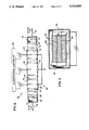
- Circuit 10 includes an RF input 12, an RF transmission line 14, and an RF output 16.
- the circuit 10 might be a radar in which case RF input 12 may represent a signal generator which launches a radar signal onto transmission line 14 for transmission to a radar antenna, in this case RF output 16.
- the radar antenna, RF output 16, may be a conventional array antenna consisting of a number of individual radiating elements suitably spaced with respect to one another.
- the relative amplitude and phase of the signals applied to each of the elements would be controlled to obtain the desired radiation pattern from the combined action of all of the elements.
- the relative phases between the elements would determine the position of the main beam which can be steered by varying the relative phase shift between the elements of the array. Changes in the relative phase of the RF signals may be readily accomplished with a variable phase shifter 20 contained in the transmission line 14.
- transmission line 14 also includes an input waveguide 22 having its input end connected to RF input 12.
- a conventional input impedance matching section 24 is connected between the output end of waveguide 22 and the input to variable phase shifter 20 to match the impedance of waveguide 22 to the impedance of the active section 26 of phase shifter 20.
- Section 24 may be a conventional quarter-wave transformer.
- the active section 26 is formed from a length of variable-permittivity material which is mounted between a pair of plate electrodes 28, 30.
- Phase shifter 20 includes an adjustable d-c voltage source V1 that is connected across electrodes 28, 30.
- phase shifter 20 is connected to an output impedance matching section 32 that impedance matches the output of phase shifter 20 to the input of waveguide 34.
- Section 32 may be designed to be similar to section 24.
- the RF output 16 is connected to the output end of waveguide 34.
- the material from which the active section 26 is formed may be any material whose permittivity may be controlled over some effective range with an applied electric field via electrodes 28, 30.
- One such material is strontium-barium titanate.
- strontium-barium titanate When formed as a single ceramic structure, strontium-barium titanate has a relatively high permittivity that can be varied when electric fields are applied thereto. Consequently, the electric length of the ceramic structure in section 26 can also be varied as a direct result of variations in the permittivity.
- the phase of RF waves propagating through the ceramic structure that forms section 26 will be subjected to various phase shifts at the exit of section 26 depending on the strength of the applied electric field and the attendant changes in permittivity.
- the electrodes 28, 30 be formed of a material that is a dielectric, having substantially the same permittivity as the ceramic material of section 26, for the RF frequencies of interest.
- the material of electrodes 28, 30 be a good conductor at d-c so as to be capable of applying the necessary electric field in response to application of control voltage V1.
- rubidium oxide may be used to fabricate electrodes 28, 30 when section 26 is formed from strontium-barium titanate.
- FIG. 2 shows an improvement over the basic ceramic phase shifter shown in FIG. 1.
- the system 40 has active impedance matching sections that, in effect, replace the passive matching sections 24, 32 of FIG. 1.
- the input active matching section consists of an initial matching section 46 followed by an active section 47.
- Section 46 transforms from the impedance of RF input section 44 to the active section 47 of phase shifter 50.
- Section 47 is fabricated of a material whose permittivity, dimensions, and range of change of permittivity are designed to form the equivalent of a quarter-wave transformer into the main active phase shift section 48.
- Section 48 similar to the active section 26 of FIG. 1, is formed of a length of variable-permittivity material.
- a control voltage source V4 is connected across section 48 via electrodes 66, 67 for purposes of varying the permittivity of the material in section 48 and thereby controlling the phase of RF energy therein.
- a variable control voltage source V2 is connected across the active phase shift section 47 via electrodes 62, 63 for varying the permittivity of the material in section 47.
- the output of section 48 is followed by an output active impedance matching section similar to the input active impedance matching section.
- the output active matching section 51 is similar in structure and function to section 47.
- the final matching section 52 is similar in structure and function to the initial matching section 46.
- a variable control voltage source V3 is connected across section 51 via electrodes 64, 65 for varying the permittivity of the material in section 51.
- the control voltage sources V2, V3, V4 are connected to a microprocessor controller 68.
- the controller 68 is used to determine the appropriate sets of voltages V2, V3, V4 to provide the desired phase shift as a function of the RF frequency while maximizing transmission through the phase shifter.
- the voltage source V2 may be adjusted to maximize RF power propagated into the main active section 48.
- the control voltage source V3 is adjustable to maximize RF power coupled out of the main active section 48.
- the external RF input transmission line 42 and RF output transmission line 56 are illustrated as being conventional RF coaxial cable or waveguide terminating in suitable structures 43, 53 to couple appropriately polarized RF energy into and out of the respective terminal areas 44, 54.
- phase shifters so far described are inherently low loss efficient structures capable of handling relatively large amounts of power.
- the phase shift is controlled by applying a voltage V1 (FIG. 1), V4 (FIG. 2) to a pair of low-loss capacitor plates (electrodes 28, 30, 66, 67).
- V1 (FIG. 1)
- V4 (FIG. 2)
- the phase shift may be controlled with a relatively small amount of control power consumption.
- large amounts of power are easily handled by these phase shifter materials.
- the sensitivity of the overall systems 10, 40 may be made significantly higher than what is attainable in conventional phase shifters.
- FIG. 3 shows a cross-sectional view of a modified phase shifter 80 having a laminated active section 83 that forms an interdigitated electrode structure.
- Active section 83 is housed in an RF cavity 85 formed by a waveguide 86.
- the RF power may be considered to be coming out of the plane of FIG. 3 with vertical polarization.
- the active material 81 e.g. strontium-barium titanate
- plate electrodes 82 which, like the electrodes 20, 28, consist of a material (e.g. rubidium oxide) which is a dielectric having approximately the same permittivity as the active material 81 at the RF but a good conductor at d-c.
- Alternate electrodes 82 are electrically connected together and brought out of opposite sides of the cavity 85 for connection to an adjustable d-c voltage source V5.
- the interdigitated electrode structure shown here may be used to reduce the mount of control voltage V5 required to produce the electric field needed to change the permittivity of the material 81.
- the active section 83 may be removed from the cavity 85 and used as a stand alone variable capacitor.
- the electrodes 82 it is not necessary to use any special material for the electrodes 82 as the effective capacitance of the device at RF is a function of the d-c voltage applied.
- the FIG. 3 structure would have a higher RF power handling capability over a conventional varactor diode.
- phase shifters so far described are primarily meant to be packaged as stand alone components. Ceramic phase shifters made in accordance with the present invention may also be made a part of an integrated circuit.
- FIGS. 4 and 5 show schematic representations of microwave or millimeter wave transmission circuits of the type typically fabricated as integrated circuits with an electronic ceramic phase shifter embedded therein.
- FIG. 4 illustrates a portion of a microwave dielectric stripline transmission circuit 90 having an active material 100 whose permittivity may be varied with changes in an electric field applied to the material 100.
- the circuit 90 also includes a stripline conductor 92 laid over input and output dielectric substrates 94, 96, and ground plane conductors 102, 104, respectively.
- Conductor 92 passes over an input impedance matching wedge 106 located between the output end of dielectric substrate 94 and the input end of material 100.
- Conductor 92 also passes over an output impedance matching wedge 108 located between the output end of material 100 and the input end of dielectric substrate 108.
- the wedges 106, 108 schematically represent conventional impedance matching dielectric materials having a graded variation in the effective dielectric constant over their length or a variation in the dielectric stripline dimensions or both.
- the conductor 92 also passes over the active material 100 (e.g. strontium-barium titanate).
- An electrode 110 is attached to the undersurface of material 100 and lies in the common plane of ground plane conductors 102, 104. Conductor 110 is appropriately spaced from conductors 102, 104.
- An adjustable d-c voltage source V6 is connected to conductor 110 via series choke coil L1 that acts as an RF isolator of d-c source V6.
- the stripline conductor 92 is held at d-c ground by an RF choke coil L2.
- the electrode 110 is RF bypassed to ground by appropriate bypass capacitor C1.
- the FIG. 4 structure operates as an RF phase shifter in the same manner described above for the FIG. 1 embodiment.
- the electrode 110 is biased with a d-c voltage from source V6 thereby creating a d-c electric field in material 100 which in turn will change the permittivity and, therefore, the electric length of material 100.
- the phase of the RF signal passing from material 100 to wedge 108 may be adjusted by adjusting the output voltage of d-c voltage source V6.
- the FIG. 4 configuration is suitable for fabrication as a microwave integrated circuit.
- FIG. 5 shows another embodiment of an integrated-circuit type configuration. This embodiment is similar to the FIG. 4 structure except that the interdigitated feature of FIG. 3 is employed.
- the use of the interdigitated electrode will be more advantageous in some cases where it is inappropriate to affect the necessary d-c level on the stripline, or it is desired to reduce the magnitude of the control voltage applied.
- the stripline transmission circuit 120 (FIG. 5) includes a stripline conductor 92, input dielectric substrate 94, output dielectric substrate 96, impedance matching wedges 106, 108, and a ground plane conductor 115 that extends continuously below substrates 94, 96 and the active portion of phase shifter 116.
- a series of parallel interdigitated electrodes 117 are embedded in the active material 118. Alternate electrodes are connected together and to opposite sides of an adjustable voltage source V7.
Abstract
Description
Claims (8)
Priority Applications (2)
| Application Number | Priority Date | Filing Date | Title |
|---|---|---|---|
| US07/425,549 US5032805A (en) | 1989-10-23 | 1989-10-23 | RF phase shifter |
| CA002028311A CA2028311C (en) | 1989-10-23 | 1990-10-23 | Rf phase shifter |
Applications Claiming Priority (1)
| Application Number | Priority Date | Filing Date | Title |
|---|---|---|---|
| US07/425,549 US5032805A (en) | 1989-10-23 | 1989-10-23 | RF phase shifter |
Publications (1)
| Publication Number | Publication Date |
|---|---|
| US5032805A true US5032805A (en) | 1991-07-16 |
Family
ID=23687043
Family Applications (1)
| Application Number | Title | Priority Date | Filing Date |
|---|---|---|---|
| US07/425,549 Expired - Fee Related US5032805A (en) | 1989-10-23 | 1989-10-23 | RF phase shifter |
Country Status (2)
| Country | Link |
|---|---|
| US (1) | US5032805A (en) |
| CA (1) | CA2028311C (en) |
Cited By (70)
| Publication number | Priority date | Publication date | Assignee | Title |
|---|---|---|---|---|
| US5206613A (en) * | 1991-11-19 | 1993-04-27 | United Technologies Corporation | Measuring the ability of electroptic materials to phase shaft RF energy |
| US5212463A (en) * | 1992-07-22 | 1993-05-18 | The United States Of America As Represented By The Secretary Of The Army | Planar ferro-electric phase shifter |
| WO1993010571A1 (en) * | 1991-11-14 | 1993-05-27 | United Technologies Corporation | Ferroelectric-scanned phased array antenna |
| WO1993012556A1 (en) * | 1991-12-13 | 1993-06-24 | United Technologies Corporation | Ferroelectric-scanned phased array antenna |
| US5289143A (en) * | 1991-07-29 | 1994-02-22 | Murata Manufacturing Co., Ltd. | Magnetostatic wave device |
| US5307033A (en) * | 1993-01-19 | 1994-04-26 | The United States Of America As Represented By The Secretary Of The Army | Planar digital ferroelectric phase shifter |
| US5334958A (en) * | 1993-07-06 | 1994-08-02 | The United States Of America As Represented By The Secretary Of The Army | Microwave ferroelectric phase shifters and methods for fabricating the same |
| EP0608889A1 (en) * | 1993-01-29 | 1994-08-03 | Hughes Aircraft Company | Phase shift device using voltage-controllable dielectrics |
| WO1994028592A1 (en) * | 1993-05-27 | 1994-12-08 | E.I. Du Pont De Nemours And Company | High tc superconductor/ferroelectric tunable microwave circuits |
| US5409889A (en) * | 1993-05-03 | 1995-04-25 | Das; Satyendranath | Ferroelectric high Tc superconductor RF phase shifter |
| US5450092A (en) * | 1993-04-26 | 1995-09-12 | Das; Satyendranath | Ferroelectric scanning RF antenna |
| EP0672308A4 (en) * | 1992-12-01 | 1995-12-13 | Superconductor Core Technologi | Tunable microwave devices incorporating high temperature superconducting and ferroelectric films. |
| US5561407A (en) * | 1995-01-31 | 1996-10-01 | The United States Of America As Represented By The Secretary Of The Army | Single substrate planar digital ferroelectric phase shifter |
| US5640042A (en) * | 1995-12-14 | 1997-06-17 | The United States Of America As Represented By The Secretary Of The Army | Thin film ferroelectric varactor |
| US5724011A (en) * | 1996-09-03 | 1998-03-03 | Hughes Electronics | Voltage variable dielectric ridged waveguide phase shifter |
| US5936484A (en) * | 1995-02-24 | 1999-08-10 | Thomson-Csf | UHF phase shifter and application to an array antenna |
| WO2001037365A1 (en) * | 1999-11-18 | 2001-05-25 | Paratek Microwave, Inc. | Rf/microwave tunable delay line |
| US6377142B1 (en) | 1998-10-16 | 2002-04-23 | Paratek Microwave, Inc. | Voltage tunable laminated dielectric materials for microwave applications |
| US6377217B1 (en) | 1999-09-14 | 2002-04-23 | Paratek Microwave, Inc. | Serially-fed phased array antennas with dielectric phase shifters |
| US6531936B1 (en) | 1998-10-16 | 2003-03-11 | Paratek Microwave, Inc. | Voltage tunable varactors and tunable devices including such varactors |
| US6538603B1 (en) * | 2000-07-21 | 2003-03-25 | Paratek Microwave, Inc. | Phased array antennas incorporating voltage-tunable phase shifters |
| US6590468B2 (en) | 2000-07-20 | 2003-07-08 | Paratek Microwave, Inc. | Tunable microwave devices with auto-adjusting matching circuit |
| US20030147576A1 (en) * | 2002-02-07 | 2003-08-07 | Fujitsu Limited | Optical waveguide device |
| US6621377B2 (en) | 2000-05-02 | 2003-09-16 | Paratek Microwave, Inc. | Microstrip phase shifter |
| US6646522B1 (en) | 1999-08-24 | 2003-11-11 | Paratek Microwave, Inc. | Voltage tunable coplanar waveguide phase shifters |
| US6710679B2 (en) | 2001-08-16 | 2004-03-23 | Paratek Microwave, Inc. | Analog rat-race phase shifters tuned by dielectric varactors |
| US6727535B1 (en) | 1998-11-09 | 2004-04-27 | Paratek Microwave, Inc. | Ferroelectric varactor with built-in DC blocks |
| US20060066414A1 (en) * | 2004-09-28 | 2006-03-30 | Rockwell Scientific Licensing, Llc | Method and apparatus for changing the polarization of a signal |
| US20060160501A1 (en) * | 2000-07-20 | 2006-07-20 | Greg Mendolia | Tunable microwave devices with auto-adjusting matching circuit |
| US20070018649A1 (en) * | 2005-07-19 | 2007-01-25 | Prsha Jeffrey A | Compact self-tuned electrical resonator for buried object locator applications |
| US20070197180A1 (en) * | 2006-01-14 | 2007-08-23 | Mckinzie William E Iii | Adaptive impedance matching module (AIMM) control architectures |
| US7352325B1 (en) | 2007-01-02 | 2008-04-01 | International Business Machines Corporation | Phase shifting and combining architecture for phased arrays |
| US20080106349A1 (en) * | 2006-11-08 | 2008-05-08 | Mckinzie William E | Adaptive impedance matching apparatus, system and method |
| US20080136714A1 (en) * | 2006-12-12 | 2008-06-12 | Daniel Boire | Antenna tuner with zero volts impedance fold back |
| US20090040687A1 (en) * | 2007-03-22 | 2009-02-12 | James Oakes | Capacitors adapted for acoustic resonance cancellation |
| US20090039976A1 (en) * | 2006-11-08 | 2009-02-12 | Mckinzie Iii William E | Adaptive impedance matching apparatus,system and method with improved dynamic range |
| US20100090760A1 (en) * | 2008-10-14 | 2010-04-15 | Paratek Microwave, Inc. | Low-distortion voltage variable capacitor assemblies |
| US20110170226A1 (en) * | 2007-03-22 | 2011-07-14 | Paratek Microwave, Inc. | Capacitors adapted for acoustic resonance cancellation |
| US7991363B2 (en) | 2007-11-14 | 2011-08-02 | Paratek Microwave, Inc. | Tuning matching circuits for transmitter and receiver bands as a function of transmitter metrics |
| US8072285B2 (en) | 2008-09-24 | 2011-12-06 | Paratek Microwave, Inc. | Methods for tuning an adaptive impedance matching network with a look-up table |
| US8125399B2 (en) | 2006-01-14 | 2012-02-28 | Paratek Microwave, Inc. | Adaptively tunable antennas incorporating an external probe to monitor radiated power |
| US8213886B2 (en) | 2007-05-07 | 2012-07-03 | Paratek Microwave, Inc. | Hybrid techniques for antenna retuning utilizing transmit and receive power information |
| US8299867B2 (en) | 2006-11-08 | 2012-10-30 | Research In Motion Rf, Inc. | Adaptive impedance matching module |
| US8325097B2 (en) | 2006-01-14 | 2012-12-04 | Research In Motion Rf, Inc. | Adaptively tunable antennas and method of operation therefore |
| US8432234B2 (en) | 2010-11-08 | 2013-04-30 | Research In Motion Rf, Inc. | Method and apparatus for tuning antennas in a communication device |
| US8472888B2 (en) | 2009-08-25 | 2013-06-25 | Research In Motion Rf, Inc. | Method and apparatus for calibrating a communication device |
| US8594584B2 (en) | 2011-05-16 | 2013-11-26 | Blackberry Limited | Method and apparatus for tuning a communication device |
| US8620236B2 (en) | 2007-04-23 | 2013-12-31 | Blackberry Limited | Techniques for improved adaptive impedance matching |
| US8626083B2 (en) | 2011-05-16 | 2014-01-07 | Blackberry Limited | Method and apparatus for tuning a communication device |
| US8655286B2 (en) | 2011-02-25 | 2014-02-18 | Blackberry Limited | Method and apparatus for tuning a communication device |
| US8693963B2 (en) | 2000-07-20 | 2014-04-08 | Blackberry Limited | Tunable microwave devices with auto-adjusting matching circuit |
| US8712340B2 (en) | 2011-02-18 | 2014-04-29 | Blackberry Limited | Method and apparatus for radio antenna frequency tuning |
| USRE44998E1 (en) | 2000-07-20 | 2014-07-08 | Blackberry Limited | Optimized thin film capacitors |
| US8803631B2 (en) | 2010-03-22 | 2014-08-12 | Blackberry Limited | Method and apparatus for adapting a variable impedance network |
| US8860526B2 (en) | 2010-04-20 | 2014-10-14 | Blackberry Limited | Method and apparatus for managing interference in a communication device |
| US8948889B2 (en) | 2012-06-01 | 2015-02-03 | Blackberry Limited | Methods and apparatus for tuning circuit components of a communication device |
| US9026062B2 (en) | 2009-10-10 | 2015-05-05 | Blackberry Limited | Method and apparatus for managing operations of a communication device |
| US9246223B2 (en) | 2012-07-17 | 2016-01-26 | Blackberry Limited | Antenna tuning for multiband operation |
| WO2016034241A1 (en) * | 2014-09-04 | 2016-03-10 | Comet Ag | Variable power capacitor for rf power applications |
| US20160099500A1 (en) * | 2014-10-06 | 2016-04-07 | Nathan Kundtz | Device, system and method to mitigate side lobes with an antenna array |
| US9350405B2 (en) | 2012-07-19 | 2016-05-24 | Blackberry Limited | Method and apparatus for antenna tuning and power consumption management in a communication device |
| US9362891B2 (en) | 2012-07-26 | 2016-06-07 | Blackberry Limited | Methods and apparatus for tuning a communication device |
| US9374113B2 (en) | 2012-12-21 | 2016-06-21 | Blackberry Limited | Method and apparatus for adjusting the timing of radio antenna tuning |
| US9406444B2 (en) | 2005-11-14 | 2016-08-02 | Blackberry Limited | Thin film capacitors |
| US9413066B2 (en) | 2012-07-19 | 2016-08-09 | Blackberry Limited | Method and apparatus for beam forming and antenna tuning in a communication device |
| US9769826B2 (en) | 2011-08-05 | 2017-09-19 | Blackberry Limited | Method and apparatus for band tuning in a communication device |
| US9853363B2 (en) | 2012-07-06 | 2017-12-26 | Blackberry Limited | Methods and apparatus to control mutual coupling between antennas |
| US10003393B2 (en) | 2014-12-16 | 2018-06-19 | Blackberry Limited | Method and apparatus for antenna selection |
| US10404295B2 (en) | 2012-12-21 | 2019-09-03 | Blackberry Limited | Method and apparatus for adjusting the timing of radio antenna tuning |
| CN112713369A (en) * | 2020-12-08 | 2021-04-27 | 北京无线电测量研究所 | Integrated ferrite phase-shifting component |
Citations (10)
| Publication number | Priority date | Publication date | Assignee | Title |
|---|---|---|---|---|
| US3466575A (en) * | 1965-07-30 | 1969-09-09 | Rca Corp | Semiconductor delay line |
| US3631501A (en) * | 1970-02-16 | 1971-12-28 | Gen Dynamics Corp | Microwave phase shifter with liquid dielectric having metallic particles in suspension |
| US3721923A (en) * | 1971-08-06 | 1973-03-20 | Rca Corp | Comprising a slab of semiconductor material |
| US3944950A (en) * | 1972-01-19 | 1976-03-16 | The United States Of America As Represented By The Secretary Of The Army | Quasi-optical integrated circuits |
| US4323901A (en) * | 1980-02-19 | 1982-04-06 | Rockwell International Corporation | Monolithic, voltage controlled, phased array |
| US4565982A (en) * | 1983-06-20 | 1986-01-21 | The United States Of America As Represented By The Secretary Of The Army | Millimeter-wave electronic phase shifter using Schottky barrier control |
| SU1352561A1 (en) * | 1983-07-13 | 1987-11-15 | МВТУ им.Н.Э.Баумана | Liquid dielectric phase shifter |
| SU1356048A1 (en) * | 1986-05-15 | 1987-11-30 | МВТУ им.Н.Э.Баумана | Phase shifter |
| US4757688A (en) * | 1986-04-01 | 1988-07-19 | Hughes Aircraft Company | Solid-state electrocaloric cooling system and method |
| US4809011A (en) * | 1985-06-14 | 1989-02-28 | Kunz Associates, Inc. | Electronically steerable antenna apparatus |
-
1989
- 1989-10-23 US US07/425,549 patent/US5032805A/en not_active Expired - Fee Related
-
1990
- 1990-10-23 CA CA002028311A patent/CA2028311C/en not_active Expired - Fee Related
Patent Citations (10)
| Publication number | Priority date | Publication date | Assignee | Title |
|---|---|---|---|---|
| US3466575A (en) * | 1965-07-30 | 1969-09-09 | Rca Corp | Semiconductor delay line |
| US3631501A (en) * | 1970-02-16 | 1971-12-28 | Gen Dynamics Corp | Microwave phase shifter with liquid dielectric having metallic particles in suspension |
| US3721923A (en) * | 1971-08-06 | 1973-03-20 | Rca Corp | Comprising a slab of semiconductor material |
| US3944950A (en) * | 1972-01-19 | 1976-03-16 | The United States Of America As Represented By The Secretary Of The Army | Quasi-optical integrated circuits |
| US4323901A (en) * | 1980-02-19 | 1982-04-06 | Rockwell International Corporation | Monolithic, voltage controlled, phased array |
| US4565982A (en) * | 1983-06-20 | 1986-01-21 | The United States Of America As Represented By The Secretary Of The Army | Millimeter-wave electronic phase shifter using Schottky barrier control |
| SU1352561A1 (en) * | 1983-07-13 | 1987-11-15 | МВТУ им.Н.Э.Баумана | Liquid dielectric phase shifter |
| US4809011A (en) * | 1985-06-14 | 1989-02-28 | Kunz Associates, Inc. | Electronically steerable antenna apparatus |
| US4757688A (en) * | 1986-04-01 | 1988-07-19 | Hughes Aircraft Company | Solid-state electrocaloric cooling system and method |
| SU1356048A1 (en) * | 1986-05-15 | 1987-11-30 | МВТУ им.Н.Э.Баумана | Phase shifter |
Cited By (176)
| Publication number | Priority date | Publication date | Assignee | Title |
|---|---|---|---|---|
| US5289143A (en) * | 1991-07-29 | 1994-02-22 | Murata Manufacturing Co., Ltd. | Magnetostatic wave device |
| WO1993010571A1 (en) * | 1991-11-14 | 1993-05-27 | United Technologies Corporation | Ferroelectric-scanned phased array antenna |
| WO1993010569A1 (en) * | 1991-11-19 | 1993-05-27 | United Technologies Corporation | An rf phase shifting device in a waveguide flange |
| US5206613A (en) * | 1991-11-19 | 1993-04-27 | United Technologies Corporation | Measuring the ability of electroptic materials to phase shaft RF energy |
| WO1993012556A1 (en) * | 1991-12-13 | 1993-06-24 | United Technologies Corporation | Ferroelectric-scanned phased array antenna |
| US5309166A (en) * | 1991-12-13 | 1994-05-03 | United Technologies Corporation | Ferroelectric-scanned phased array antenna |
| US5212463A (en) * | 1992-07-22 | 1993-05-18 | The United States Of America As Represented By The Secretary Of The Army | Planar ferro-electric phase shifter |
| EP0672308A4 (en) * | 1992-12-01 | 1995-12-13 | Superconductor Core Technologi | Tunable microwave devices incorporating high temperature superconducting and ferroelectric films. |
| US5307033A (en) * | 1993-01-19 | 1994-04-26 | The United States Of America As Represented By The Secretary Of The Army | Planar digital ferroelectric phase shifter |
| AU657646B2 (en) * | 1993-01-29 | 1995-03-16 | Hughes Aircraft Company | Phase shift device using voltage-controllable dielectrics |
| EP0608889A1 (en) * | 1993-01-29 | 1994-08-03 | Hughes Aircraft Company | Phase shift device using voltage-controllable dielectrics |
| US5355104A (en) * | 1993-01-29 | 1994-10-11 | Hughes Aircraft Company | Phase shift device using voltage-controllable dielectrics |
| US5450092A (en) * | 1993-04-26 | 1995-09-12 | Das; Satyendranath | Ferroelectric scanning RF antenna |
| US5409889A (en) * | 1993-05-03 | 1995-04-25 | Das; Satyendranath | Ferroelectric high Tc superconductor RF phase shifter |
| WO1994028592A1 (en) * | 1993-05-27 | 1994-12-08 | E.I. Du Pont De Nemours And Company | High tc superconductor/ferroelectric tunable microwave circuits |
| US5334958A (en) * | 1993-07-06 | 1994-08-02 | The United States Of America As Represented By The Secretary Of The Army | Microwave ferroelectric phase shifters and methods for fabricating the same |
| US5561407A (en) * | 1995-01-31 | 1996-10-01 | The United States Of America As Represented By The Secretary Of The Army | Single substrate planar digital ferroelectric phase shifter |
| US5936484A (en) * | 1995-02-24 | 1999-08-10 | Thomson-Csf | UHF phase shifter and application to an array antenna |
| US5640042A (en) * | 1995-12-14 | 1997-06-17 | The United States Of America As Represented By The Secretary Of The Army | Thin film ferroelectric varactor |
| US5724011A (en) * | 1996-09-03 | 1998-03-03 | Hughes Electronics | Voltage variable dielectric ridged waveguide phase shifter |
| US6377142B1 (en) | 1998-10-16 | 2002-04-23 | Paratek Microwave, Inc. | Voltage tunable laminated dielectric materials for microwave applications |
| US6531936B1 (en) | 1998-10-16 | 2003-03-11 | Paratek Microwave, Inc. | Voltage tunable varactors and tunable devices including such varactors |
| US6686814B2 (en) | 1998-10-16 | 2004-02-03 | Paratek Microwave, Inc. | Voltage tunable varactors and tunable devices including such varactors |
| US6727535B1 (en) | 1998-11-09 | 2004-04-27 | Paratek Microwave, Inc. | Ferroelectric varactor with built-in DC blocks |
| US6954118B2 (en) | 1999-08-24 | 2005-10-11 | Paratek Microwave, Inc. | Voltage tunable coplanar phase shifters with a conductive dome structure |
| US6646522B1 (en) | 1999-08-24 | 2003-11-11 | Paratek Microwave, Inc. | Voltage tunable coplanar waveguide phase shifters |
| US20040036553A1 (en) * | 1999-08-24 | 2004-02-26 | Andrey Kozyrev | Voltage tunable coplanar phase shifters |
| US6377217B1 (en) | 1999-09-14 | 2002-04-23 | Paratek Microwave, Inc. | Serially-fed phased array antennas with dielectric phase shifters |
| WO2001037365A1 (en) * | 1999-11-18 | 2001-05-25 | Paratek Microwave, Inc. | Rf/microwave tunable delay line |
| US6556102B1 (en) | 1999-11-18 | 2003-04-29 | Paratek Microwave, Inc. | RF/microwave tunable delay line |
| US6621377B2 (en) | 2000-05-02 | 2003-09-16 | Paratek Microwave, Inc. | Microstrip phase shifter |
| US6864757B2 (en) | 2000-07-20 | 2005-03-08 | Paratek Microwave, Inc. | Tunable microwave devices with auto-adjusting matching circuit |
| US20080169995A1 (en) * | 2000-07-20 | 2008-07-17 | Cornelis Frederik Du Toit | Tunable microwave devices with auto-adjusting matching circuit |
| US7728693B2 (en) | 2000-07-20 | 2010-06-01 | Paratek Microwave, Inc. | Tunable microwave devices with auto-adjusting matching circuit |
| US8896391B2 (en) | 2000-07-20 | 2014-11-25 | Blackberry Limited | Tunable microwave devices with auto-adjusting matching circuit |
| US6759918B2 (en) | 2000-07-20 | 2004-07-06 | Paratek Microwave, Inc. | Tunable microwave devices with auto-adjusting matching circuit |
| US8693963B2 (en) | 2000-07-20 | 2014-04-08 | Blackberry Limited | Tunable microwave devices with auto-adjusting matching circuit |
| US20050110593A1 (en) * | 2000-07-20 | 2005-05-26 | Du Toit Cornelis F. | Tunable microwave devices with auto-adjusting matching circuit |
| US6590468B2 (en) | 2000-07-20 | 2003-07-08 | Paratek Microwave, Inc. | Tunable microwave devices with auto-adjusting matching circuit |
| US9431990B2 (en) | 2000-07-20 | 2016-08-30 | Blackberry Limited | Tunable microwave devices with auto-adjusting matching circuit |
| US20060160501A1 (en) * | 2000-07-20 | 2006-07-20 | Greg Mendolia | Tunable microwave devices with auto-adjusting matching circuit |
| US20060226929A1 (en) * | 2000-07-20 | 2006-10-12 | Du Toit Cornelis F | Tunable microwave devices with auto-adjusting matching circuit |
| US20030210105A1 (en) * | 2000-07-20 | 2003-11-13 | Du Toit Cornelis Frederik | Tunable microwave devices with auto-adjusting matching circuit |
| US20070146094A1 (en) * | 2000-07-20 | 2007-06-28 | Cornelis Frederik Du Toit | Tunable microwave devices with auto-adjusting matching circuit |
| US9768752B2 (en) | 2000-07-20 | 2017-09-19 | Blackberry Limited | Tunable microwave devices with auto-adjusting matching circuit |
| US7969257B2 (en) | 2000-07-20 | 2011-06-28 | Paratek Microwave, Inc. | Tunable microwave devices with auto-adjusting matching circuit |
| US7865154B2 (en) | 2000-07-20 | 2011-01-04 | Paratek Microwave, Inc. | Tunable microwave devices with auto-adjusting matching circuit |
| US8744384B2 (en) | 2000-07-20 | 2014-06-03 | Blackberry Limited | Tunable microwave devices with auto-adjusting matching circuit |
| USRE44998E1 (en) | 2000-07-20 | 2014-07-08 | Blackberry Limited | Optimized thin film capacitors |
| US9948270B2 (en) | 2000-07-20 | 2018-04-17 | Blackberry Limited | Tunable microwave devices with auto-adjusting matching circuit |
| US7714678B2 (en) | 2000-07-20 | 2010-05-11 | Paratek Microwave, Inc. | Tunable microwave devices with auto-adjusting matching circuit |
| US7795990B2 (en) | 2000-07-20 | 2010-09-14 | Paratek Microwave, Inc. | Tunable microwave devices with auto-adjusting matching circuit |
| US6538603B1 (en) * | 2000-07-21 | 2003-03-25 | Paratek Microwave, Inc. | Phased array antennas incorporating voltage-tunable phase shifters |
| US6710679B2 (en) | 2001-08-16 | 2004-03-23 | Paratek Microwave, Inc. | Analog rat-race phase shifters tuned by dielectric varactors |
| US7239764B2 (en) * | 2002-02-07 | 2007-07-03 | Fujitsu Limited | Optical waveguide device with reduced driving voltage |
| US20030147576A1 (en) * | 2002-02-07 | 2003-08-07 | Fujitsu Limited | Optical waveguide device |
| US7414491B2 (en) * | 2004-09-28 | 2008-08-19 | Teledyne Licensing, Llc | Method and apparatus for changing the polarization of a signal |
| US20060066414A1 (en) * | 2004-09-28 | 2006-03-30 | Rockwell Scientific Licensing, Llc | Method and apparatus for changing the polarization of a signal |
| US20070018649A1 (en) * | 2005-07-19 | 2007-01-25 | Prsha Jeffrey A | Compact self-tuned electrical resonator for buried object locator applications |
| US7276910B2 (en) | 2005-07-19 | 2007-10-02 | Seektech, Inc. | Compact self-tuned electrical resonator for buried object locator applications |
| US10163574B2 (en) | 2005-11-14 | 2018-12-25 | Blackberry Limited | Thin films capacitors |
| US9406444B2 (en) | 2005-11-14 | 2016-08-02 | Blackberry Limited | Thin film capacitors |
| US20070197180A1 (en) * | 2006-01-14 | 2007-08-23 | Mckinzie William E Iii | Adaptive impedance matching module (AIMM) control architectures |
| US9853622B2 (en) | 2006-01-14 | 2017-12-26 | Blackberry Limited | Adaptive matching network |
| US7711337B2 (en) | 2006-01-14 | 2010-05-04 | Paratek Microwave, Inc. | Adaptive impedance matching module (AIMM) control architectures |
| US10177731B2 (en) | 2006-01-14 | 2019-01-08 | Blackberry Limited | Adaptive matching network |
| US8942657B2 (en) | 2006-01-14 | 2015-01-27 | Blackberry Limited | Adaptive matching network |
| US20100156552A1 (en) * | 2006-01-14 | 2010-06-24 | Paratek Microwave, Inc. | Adaptive matching network |
| US8269683B2 (en) | 2006-01-14 | 2012-09-18 | Research In Motion Rf, Inc. | Adaptively tunable antennas and method of operation therefore |
| US8620246B2 (en) | 2006-01-14 | 2013-12-31 | Blackberry Limited | Adaptive impedance matching module (AIMM) control architectures |
| US8620247B2 (en) | 2006-01-14 | 2013-12-31 | Blackberry Limited | Adaptive impedance matching module (AIMM) control architectures |
| US8463218B2 (en) | 2006-01-14 | 2013-06-11 | Research In Motion Rf, Inc. | Adaptive matching network |
| US8405563B2 (en) | 2006-01-14 | 2013-03-26 | Research In Motion Rf, Inc. | Adaptively tunable antennas incorporating an external probe to monitor radiated power |
| US8125399B2 (en) | 2006-01-14 | 2012-02-28 | Paratek Microwave, Inc. | Adaptively tunable antennas incorporating an external probe to monitor radiated power |
| US8325097B2 (en) | 2006-01-14 | 2012-12-04 | Research In Motion Rf, Inc. | Adaptively tunable antennas and method of operation therefore |
| US9419581B2 (en) | 2006-11-08 | 2016-08-16 | Blackberry Limited | Adaptive impedance matching apparatus, system and method with improved dynamic range |
| US20080106349A1 (en) * | 2006-11-08 | 2008-05-08 | Mckinzie William E | Adaptive impedance matching apparatus, system and method |
| US8217731B2 (en) | 2006-11-08 | 2012-07-10 | Paratek Microwave, Inc. | Method and apparatus for adaptive impedance matching |
| US8299867B2 (en) | 2006-11-08 | 2012-10-30 | Research In Motion Rf, Inc. | Adaptive impedance matching module |
| US20100164639A1 (en) * | 2006-11-08 | 2010-07-01 | Paratek Microwave, Inc. | Method and apparatus for adaptive impedance matching |
| US9130543B2 (en) | 2006-11-08 | 2015-09-08 | Blackberry Limited | Method and apparatus for adaptive impedance matching |
| US7852170B2 (en) | 2006-11-08 | 2010-12-14 | Paratek Microwave, Inc. | Adaptive impedance matching apparatus, system and method with improved dynamic range |
| US20090039976A1 (en) * | 2006-11-08 | 2009-02-12 | Mckinzie Iii William E | Adaptive impedance matching apparatus,system and method with improved dynamic range |
| US20100164641A1 (en) * | 2006-11-08 | 2010-07-01 | Paratek Microwave, Inc. | Method and apparatus for adaptive impedance matching |
| US8680934B2 (en) | 2006-11-08 | 2014-03-25 | Blackberry Limited | System for establishing communication with a mobile device server |
| US10050598B2 (en) | 2006-11-08 | 2018-08-14 | Blackberry Limited | Method and apparatus for adaptive impedance matching |
| US7714676B2 (en) | 2006-11-08 | 2010-05-11 | Paratek Microwave, Inc. | Adaptive impedance matching apparatus, system and method |
| US10020828B2 (en) | 2006-11-08 | 2018-07-10 | Blackberry Limited | Adaptive impedance matching apparatus, system and method with improved dynamic range |
| US8217732B2 (en) | 2006-11-08 | 2012-07-10 | Paratek Microwave, Inc. | Method and apparatus for adaptive impedance matching |
| US8558633B2 (en) | 2006-11-08 | 2013-10-15 | Blackberry Limited | Method and apparatus for adaptive impedance matching |
| US8564381B2 (en) | 2006-11-08 | 2013-10-22 | Blackberry Limited | Method and apparatus for adaptive impedance matching |
| US9722577B2 (en) | 2006-11-08 | 2017-08-01 | Blackberry Limited | Method and apparatus for adaptive impedance matching |
| US8008982B2 (en) | 2006-11-08 | 2011-08-30 | Paratek Microwave, Inc. | Method and apparatus for adaptive impedance matching |
| US20080136714A1 (en) * | 2006-12-12 | 2008-06-12 | Daniel Boire | Antenna tuner with zero volts impedance fold back |
| US7813777B2 (en) | 2006-12-12 | 2010-10-12 | Paratek Microwave, Inc. | Antenna tuner with zero volts impedance fold back |
| US7683833B2 (en) | 2007-01-02 | 2010-03-23 | International Business Machines Corporation | Phase shifting and combining architecture for phased arrays |
| US7352325B1 (en) | 2007-01-02 | 2008-04-01 | International Business Machines Corporation | Phase shifting and combining architecture for phased arrays |
| US9142355B2 (en) | 2007-03-22 | 2015-09-22 | Blackberry Limited | Capacitors adapted for acoustic resonance cancellation |
| US9269496B2 (en) | 2007-03-22 | 2016-02-23 | Blackberry Limited | Capacitors adapted for acoustic resonance cancellation |
| US20110170226A1 (en) * | 2007-03-22 | 2011-07-14 | Paratek Microwave, Inc. | Capacitors adapted for acoustic resonance cancellation |
| US20090040687A1 (en) * | 2007-03-22 | 2009-02-12 | James Oakes | Capacitors adapted for acoustic resonance cancellation |
| US8467169B2 (en) * | 2007-03-22 | 2013-06-18 | Research In Motion Rf, Inc. | Capacitors adapted for acoustic resonance cancellation |
| US8400752B2 (en) | 2007-03-22 | 2013-03-19 | Research In Motion Rf, Inc. | Capacitors adapted for acoustic resonance cancellation |
| US8953299B2 (en) | 2007-03-22 | 2015-02-10 | Blackberry Limited | Capacitors adapted for acoustic resonance cancellation |
| US9698748B2 (en) | 2007-04-23 | 2017-07-04 | Blackberry Limited | Adaptive impedance matching |
| US8620236B2 (en) | 2007-04-23 | 2013-12-31 | Blackberry Limited | Techniques for improved adaptive impedance matching |
| US8457569B2 (en) | 2007-05-07 | 2013-06-04 | Research In Motion Rf, Inc. | Hybrid techniques for antenna retuning utilizing transmit and receive power information |
| US8781417B2 (en) | 2007-05-07 | 2014-07-15 | Blackberry Limited | Hybrid techniques for antenna retuning utilizing transmit and receive power information |
| US9119152B2 (en) | 2007-05-07 | 2015-08-25 | Blackberry Limited | Hybrid techniques for antenna retuning utilizing transmit and receive power information |
| US8213886B2 (en) | 2007-05-07 | 2012-07-03 | Paratek Microwave, Inc. | Hybrid techniques for antenna retuning utilizing transmit and receive power information |
| USRE48435E1 (en) | 2007-11-14 | 2021-02-09 | Nxp Usa, Inc. | Tuning matching circuits for transmitter and receiver bands as a function of the transmitter metrics |
| US7991363B2 (en) | 2007-11-14 | 2011-08-02 | Paratek Microwave, Inc. | Tuning matching circuits for transmitter and receiver bands as a function of transmitter metrics |
| US8428523B2 (en) | 2007-11-14 | 2013-04-23 | Research In Motion Rf, Inc. | Tuning matching circuits for transmitter and receiver bands as a function of transmitter metrics |
| USRE47412E1 (en) | 2007-11-14 | 2019-05-28 | Blackberry Limited | Tuning matching circuits for transmitter and receiver bands as a function of the transmitter metrics |
| US8798555B2 (en) | 2007-11-14 | 2014-08-05 | Blackberry Limited | Tuning matching circuits for transmitter and receiver bands as a function of the transmitter metrics |
| US8674783B2 (en) | 2008-09-24 | 2014-03-18 | Blackberry Limited | Methods for tuning an adaptive impedance matching network with a look-up table |
| US9698758B2 (en) | 2008-09-24 | 2017-07-04 | Blackberry Limited | Methods for tuning an adaptive impedance matching network with a look-up table |
| US8421548B2 (en) | 2008-09-24 | 2013-04-16 | Research In Motion Rf, Inc. | Methods for tuning an adaptive impedance matching network with a look-up table |
| US8957742B2 (en) | 2008-09-24 | 2015-02-17 | Blackberry Limited | Methods for tuning an adaptive impedance matching network with a look-up table |
| US8072285B2 (en) | 2008-09-24 | 2011-12-06 | Paratek Microwave, Inc. | Methods for tuning an adaptive impedance matching network with a look-up table |
| US20100090760A1 (en) * | 2008-10-14 | 2010-04-15 | Paratek Microwave, Inc. | Low-distortion voltage variable capacitor assemblies |
| US8067858B2 (en) | 2008-10-14 | 2011-11-29 | Paratek Microwave, Inc. | Low-distortion voltage variable capacitor assemblies |
| US8472888B2 (en) | 2009-08-25 | 2013-06-25 | Research In Motion Rf, Inc. | Method and apparatus for calibrating a communication device |
| US8787845B2 (en) | 2009-08-25 | 2014-07-22 | Blackberry Limited | Method and apparatus for calibrating a communication device |
| US9020446B2 (en) | 2009-08-25 | 2015-04-28 | Blackberry Limited | Method and apparatus for calibrating a communication device |
| US10659088B2 (en) | 2009-10-10 | 2020-05-19 | Nxp Usa, Inc. | Method and apparatus for managing operations of a communication device |
| US9853663B2 (en) | 2009-10-10 | 2017-12-26 | Blackberry Limited | Method and apparatus for managing operations of a communication device |
| US9026062B2 (en) | 2009-10-10 | 2015-05-05 | Blackberry Limited | Method and apparatus for managing operations of a communication device |
| US10615769B2 (en) | 2010-03-22 | 2020-04-07 | Blackberry Limited | Method and apparatus for adapting a variable impedance network |
| US10263595B2 (en) | 2010-03-22 | 2019-04-16 | Blackberry Limited | Method and apparatus for adapting a variable impedance network |
| US9742375B2 (en) | 2010-03-22 | 2017-08-22 | Blackberry Limited | Method and apparatus for adapting a variable impedance network |
| US9548716B2 (en) | 2010-03-22 | 2017-01-17 | Blackberry Limited | Method and apparatus for adapting a variable impedance network |
| US8803631B2 (en) | 2010-03-22 | 2014-08-12 | Blackberry Limited | Method and apparatus for adapting a variable impedance network |
| US9608591B2 (en) | 2010-03-22 | 2017-03-28 | Blackberry Limited | Method and apparatus for adapting a variable impedance network |
| US9450637B2 (en) | 2010-04-20 | 2016-09-20 | Blackberry Limited | Method and apparatus for managing interference in a communication device |
| US8860525B2 (en) | 2010-04-20 | 2014-10-14 | Blackberry Limited | Method and apparatus for managing interference in a communication device |
| US9564944B2 (en) | 2010-04-20 | 2017-02-07 | Blackberry Limited | Method and apparatus for managing interference in a communication device |
| US9941922B2 (en) | 2010-04-20 | 2018-04-10 | Blackberry Limited | Method and apparatus for managing interference in a communication device |
| US8860526B2 (en) | 2010-04-20 | 2014-10-14 | Blackberry Limited | Method and apparatus for managing interference in a communication device |
| US8432234B2 (en) | 2010-11-08 | 2013-04-30 | Research In Motion Rf, Inc. | Method and apparatus for tuning antennas in a communication device |
| US9379454B2 (en) | 2010-11-08 | 2016-06-28 | Blackberry Limited | Method and apparatus for tuning antennas in a communication device |
| US9263806B2 (en) | 2010-11-08 | 2016-02-16 | Blackberry Limited | Method and apparatus for tuning antennas in a communication device |
| US9935674B2 (en) | 2011-02-18 | 2018-04-03 | Blackberry Limited | Method and apparatus for radio antenna frequency tuning |
| US9698858B2 (en) | 2011-02-18 | 2017-07-04 | Blackberry Limited | Method and apparatus for radio antenna frequency tuning |
| US8712340B2 (en) | 2011-02-18 | 2014-04-29 | Blackberry Limited | Method and apparatus for radio antenna frequency tuning |
| US10979095B2 (en) | 2011-02-18 | 2021-04-13 | Nxp Usa, Inc. | Method and apparatus for radio antenna frequency tuning |
| US9231643B2 (en) | 2011-02-18 | 2016-01-05 | Blackberry Limited | Method and apparatus for radio antenna frequency tuning |
| US9473216B2 (en) | 2011-02-25 | 2016-10-18 | Blackberry Limited | Method and apparatus for tuning a communication device |
| US8655286B2 (en) | 2011-02-25 | 2014-02-18 | Blackberry Limited | Method and apparatus for tuning a communication device |
| US8594584B2 (en) | 2011-05-16 | 2013-11-26 | Blackberry Limited | Method and apparatus for tuning a communication device |
| US9716311B2 (en) | 2011-05-16 | 2017-07-25 | Blackberry Limited | Method and apparatus for tuning a communication device |
| US8626083B2 (en) | 2011-05-16 | 2014-01-07 | Blackberry Limited | Method and apparatus for tuning a communication device |
| US10218070B2 (en) | 2011-05-16 | 2019-02-26 | Blackberry Limited | Method and apparatus for tuning a communication device |
| US9769826B2 (en) | 2011-08-05 | 2017-09-19 | Blackberry Limited | Method and apparatus for band tuning in a communication device |
| US10624091B2 (en) | 2011-08-05 | 2020-04-14 | Blackberry Limited | Method and apparatus for band tuning in a communication device |
| US9671765B2 (en) | 2012-06-01 | 2017-06-06 | Blackberry Limited | Methods and apparatus for tuning circuit components of a communication device |
| US8948889B2 (en) | 2012-06-01 | 2015-02-03 | Blackberry Limited | Methods and apparatus for tuning circuit components of a communication device |
| US9853363B2 (en) | 2012-07-06 | 2017-12-26 | Blackberry Limited | Methods and apparatus to control mutual coupling between antennas |
| US9246223B2 (en) | 2012-07-17 | 2016-01-26 | Blackberry Limited | Antenna tuning for multiband operation |
| US9350405B2 (en) | 2012-07-19 | 2016-05-24 | Blackberry Limited | Method and apparatus for antenna tuning and power consumption management in a communication device |
| US9941910B2 (en) | 2012-07-19 | 2018-04-10 | Blackberry Limited | Method and apparatus for antenna tuning and power consumption management in a communication device |
| US9413066B2 (en) | 2012-07-19 | 2016-08-09 | Blackberry Limited | Method and apparatus for beam forming and antenna tuning in a communication device |
| US9362891B2 (en) | 2012-07-26 | 2016-06-07 | Blackberry Limited | Methods and apparatus for tuning a communication device |
| US9374113B2 (en) | 2012-12-21 | 2016-06-21 | Blackberry Limited | Method and apparatus for adjusting the timing of radio antenna tuning |
| US10404295B2 (en) | 2012-12-21 | 2019-09-03 | Blackberry Limited | Method and apparatus for adjusting the timing of radio antenna tuning |
| US10700719B2 (en) | 2012-12-21 | 2020-06-30 | Nxp Usa, Inc. | Method and apparatus for adjusting the timing of radio antenna tuning |
| US9768810B2 (en) | 2012-12-21 | 2017-09-19 | Blackberry Limited | Method and apparatus for adjusting the timing of radio antenna tuning |
| WO2016034241A1 (en) * | 2014-09-04 | 2016-03-10 | Comet Ag | Variable power capacitor for rf power applications |
| US11011350B2 (en) | 2014-09-04 | 2021-05-18 | Comet Ag | Variable power capacitor for RF power applications |
| US10263331B2 (en) * | 2014-10-06 | 2019-04-16 | Kymeta Corporation | Device, system and method to mitigate side lobes with an antenna array |
| US20160099500A1 (en) * | 2014-10-06 | 2016-04-07 | Nathan Kundtz | Device, system and method to mitigate side lobes with an antenna array |
| US11450955B2 (en) | 2014-10-06 | 2022-09-20 | Kymeta Corporation | Device, system and method to mitigate side lobes with an antenna array |
| US10651918B2 (en) | 2014-12-16 | 2020-05-12 | Nxp Usa, Inc. | Method and apparatus for antenna selection |
| US10003393B2 (en) | 2014-12-16 | 2018-06-19 | Blackberry Limited | Method and apparatus for antenna selection |
| CN112713369A (en) * | 2020-12-08 | 2021-04-27 | 北京无线电测量研究所 | Integrated ferrite phase-shifting component |
| CN112713369B (en) * | 2020-12-08 | 2021-12-10 | 北京无线电测量研究所 | Integrated ferrite phase-shifting component |
Also Published As
| Publication number | Publication date |
|---|---|
| CA2028311A1 (en) | 1991-04-24 |
| CA2028311C (en) | 1994-08-02 |
Similar Documents
| Publication | Publication Date | Title |
|---|---|---|
| US5032805A (en) | RF phase shifter | |
| US5212463A (en) | Planar ferro-electric phase shifter | |
| US5307033A (en) | Planar digital ferroelectric phase shifter | |
| US5309166A (en) | Ferroelectric-scanned phased array antenna | |
| US5504466A (en) | Suspended dielectric and microstrip type microwave phase shifter and application to lobe scanning antenne networks | |
| US4845449A (en) | Millimeter wave microstrip modulator/switch | |
| JP2650844B2 (en) | Phase shift device using voltage controllable dielectric | |
| US4859972A (en) | Continuous phase shifter for a phased array hyperthermia system | |
| US5450092A (en) | Ferroelectric scanning RF antenna | |
| US4105959A (en) | Amplitude balanced diode phase shifter | |
| Varadan et al. | A novel microwave planar phase shifter | |
| EP3275041B1 (en) | Phase shifter | |
| US5136304A (en) | Electronically tunable phased array element | |
| US8279129B1 (en) | Transverse device phase shifter | |
| Yun et al. | A low-loss time-delay phase shifter controlled by piezoelectric transducer to perturb microstrip line | |
| JPH11103201A (en) | Phase shifter, phase shifter array and phased array antenna system | |
| Demidov et al. | Electrical tuning of dispersion characteristics of surface electromagnetic-spin waves propagating in ferrite-ferroelectric layered structures | |
| RU2666969C1 (en) | Nonlinear divider of uhf signal power on spin waves | |
| US5153171A (en) | Superconducting variable phase shifter using squid's to effect phase shift | |
| US4405907A (en) | Controllable phase shifter comprising gyromagnetic and non-gyromagnetic sections | |
| US4020429A (en) | High power radio frequency tunable circuits | |
| US7382215B1 (en) | Image guide coupler switch | |
| US5206613A (en) | Measuring the ability of electroptic materials to phase shaft RF energy | |
| US4816787A (en) | Millimeter wave microstrip phase shifter | |
| US3760304A (en) | Slot line |
Legal Events
| Date | Code | Title | Description |
|---|---|---|---|
| AS | Assignment |
Owner name: GOVERNMENT OF THE UNITED STATES OF AMERICA, AS REP Free format text: ASSIGNMENT OF ASSIGNORS INTEREST.;ASSIGNOR:ELMER, FRANK J.;REEL/FRAME:005693/0974 Effective date: 19900119 |
|
| FEPP | Fee payment procedure |
Free format text: PAYOR NUMBER ASSIGNED (ORIGINAL EVENT CODE: ASPN); ENTITY STATUS OF PATENT OWNER: LARGE ENTITY |
|
| REMI | Maintenance fee reminder mailed | ||
| FPAY | Fee payment |
Year of fee payment: 4 |
|
| SULP | Surcharge for late payment | ||
| REMI | Maintenance fee reminder mailed | ||
| FPAY | Fee payment |
Year of fee payment: 8 |
|
| SULP | Surcharge for late payment | ||
| LAPS | Lapse for failure to pay maintenance fees | ||
| FP | Lapsed due to failure to pay maintenance fee |
Effective date: 20030716 |
|
| STCH | Information on status: patent discontinuation |
Free format text: PATENT EXPIRED DUE TO NONPAYMENT OF MAINTENANCE FEES UNDER 37 CFR 1.362 |