US5109262A - Bipolar transistor with reduced collector resistance - Google Patents

Bipolar transistor with reduced collector resistance Download PDF

Info

Publication number
US5109262A
US5109262A US07/565,494 US56549490A US5109262A US 5109262 A US5109262 A US 5109262A US 56549490 A US56549490 A US 56549490A US 5109262 A US5109262 A US 5109262A
Authority
US
United States
Prior art keywords
collector
transistor
impurity region
trench
conductivity type
Prior art date
Legal status (The legal status is an assumption and is not a legal conclusion. Google has not performed a legal analysis and makes no representation as to the accuracy of the status listed.)
Expired - Fee Related
Application number
US07/565,494
Inventor
Yasuo Kadota
Junzoh Shimizu
Current Assignee (The listed assignees may be inaccurate. Google has not performed a legal analysis and makes no representation or warranty as to the accuracy of the list.)
NEC Corp
Original Assignee
NEC Corp
Priority date (The priority date is an assumption and is not a legal conclusion. Google has not performed a legal analysis and makes no representation as to the accuracy of the date listed.)
Filing date
Publication date
Application filed by NEC Corp filed Critical NEC Corp
Application granted granted Critical
Publication of US5109262A publication Critical patent/US5109262A/en
Anticipated expiration legal-status Critical
Expired - Fee Related legal-status Critical Current

Links

Images

Classifications

    • HELECTRICITY
    • H01ELECTRIC ELEMENTS
    • H01LSEMICONDUCTOR DEVICES NOT COVERED BY CLASS H10
    • H01L21/00Processes or apparatus adapted for the manufacture or treatment of semiconductor or solid state devices or of parts thereof
    • H01L21/70Manufacture or treatment of devices consisting of a plurality of solid state components formed in or on a common substrate or of parts thereof; Manufacture of integrated circuit devices or of parts thereof
    • H01L21/71Manufacture of specific parts of devices defined in group H01L21/70
    • H01L21/768Applying interconnections to be used for carrying current between separate components within a device comprising conductors and dielectrics
    • H01L21/76897Formation of self-aligned vias or contact plugs, i.e. involving a lithographically uncritical step
    • HELECTRICITY
    • H01ELECTRIC ELEMENTS
    • H01LSEMICONDUCTOR DEVICES NOT COVERED BY CLASS H10
    • H01L21/00Processes or apparatus adapted for the manufacture or treatment of semiconductor or solid state devices or of parts thereof
    • H01L21/02Manufacture or treatment of semiconductor devices or of parts thereof
    • H01L21/04Manufacture or treatment of semiconductor devices or of parts thereof the devices having at least one potential-jump barrier or surface barrier, e.g. PN junction, depletion layer or carrier concentration layer
    • H01L21/18Manufacture or treatment of semiconductor devices or of parts thereof the devices having at least one potential-jump barrier or surface barrier, e.g. PN junction, depletion layer or carrier concentration layer the devices having semiconductor bodies comprising elements of Group IV of the Periodic System or AIIIBV compounds with or without impurities, e.g. doping materials
    • H01L21/28Manufacture of electrodes on semiconductor bodies using processes or apparatus not provided for in groups H01L21/20 - H01L21/268
    • H01L21/283Deposition of conductive or insulating materials for electrodes conducting electric current
    • H01L21/285Deposition of conductive or insulating materials for electrodes conducting electric current from a gas or vapour, e.g. condensation
    • H01L21/28506Deposition of conductive or insulating materials for electrodes conducting electric current from a gas or vapour, e.g. condensation of conductive layers
    • H01L21/28512Deposition of conductive or insulating materials for electrodes conducting electric current from a gas or vapour, e.g. condensation of conductive layers on semiconductor bodies comprising elements of Group IV of the Periodic System
    • H01L21/28525Deposition of conductive or insulating materials for electrodes conducting electric current from a gas or vapour, e.g. condensation of conductive layers on semiconductor bodies comprising elements of Group IV of the Periodic System the conductive layers comprising semiconducting material
    • HELECTRICITY
    • H01ELECTRIC ELEMENTS
    • H01LSEMICONDUCTOR DEVICES NOT COVERED BY CLASS H10
    • H01L21/00Processes or apparatus adapted for the manufacture or treatment of semiconductor or solid state devices or of parts thereof
    • H01L21/70Manufacture or treatment of devices consisting of a plurality of solid state components formed in or on a common substrate or of parts thereof; Manufacture of integrated circuit devices or of parts thereof
    • H01L21/71Manufacture of specific parts of devices defined in group H01L21/70
    • H01L21/76Making of isolation regions between components
    • H01L21/762Dielectric regions, e.g. EPIC dielectric isolation, LOCOS; Trench refilling techniques, SOI technology, use of channel stoppers
    • H01L21/76224Dielectric regions, e.g. EPIC dielectric isolation, LOCOS; Trench refilling techniques, SOI technology, use of channel stoppers using trench refilling with dielectric materials
    • HELECTRICITY
    • H01ELECTRIC ELEMENTS
    • H01LSEMICONDUCTOR DEVICES NOT COVERED BY CLASS H10
    • H01L29/00Semiconductor devices adapted for rectifying, amplifying, oscillating or switching, or capacitors or resistors with at least one potential-jump barrier or surface barrier, e.g. PN junction depletion layer or carrier concentration layer; Details of semiconductor bodies or of electrodes thereof  ; Multistep manufacturing processes therefor
    • H01L29/02Semiconductor bodies ; Multistep manufacturing processes therefor
    • H01L29/06Semiconductor bodies ; Multistep manufacturing processes therefor characterised by their shape; characterised by the shapes, relative sizes, or dispositions of the semiconductor regions ; characterised by the concentration or distribution of impurities within semiconductor regions
    • H01L29/0603Semiconductor bodies ; Multistep manufacturing processes therefor characterised by their shape; characterised by the shapes, relative sizes, or dispositions of the semiconductor regions ; characterised by the concentration or distribution of impurities within semiconductor regions characterised by particular constructional design considerations, e.g. for preventing surface leakage, for controlling electric field concentration or for internal isolations regions
    • H01L29/0642Isolation within the component, i.e. internal isolation
    • H01L29/0649Dielectric regions, e.g. SiO2 regions, air gaps
    • HELECTRICITY
    • H01ELECTRIC ELEMENTS
    • H01LSEMICONDUCTOR DEVICES NOT COVERED BY CLASS H10
    • H01L29/00Semiconductor devices adapted for rectifying, amplifying, oscillating or switching, or capacitors or resistors with at least one potential-jump barrier or surface barrier, e.g. PN junction depletion layer or carrier concentration layer; Details of semiconductor bodies or of electrodes thereof  ; Multistep manufacturing processes therefor
    • H01L29/66Types of semiconductor device ; Multistep manufacturing processes therefor
    • H01L29/66007Multistep manufacturing processes
    • H01L29/66075Multistep manufacturing processes of devices having semiconductor bodies comprising group 14 or group 13/15 materials
    • H01L29/66227Multistep manufacturing processes of devices having semiconductor bodies comprising group 14 or group 13/15 materials the devices being controllable only by the electric current supplied or the electric potential applied, to an electrode which does not carry the current to be rectified, amplified or switched, e.g. three-terminal devices
    • H01L29/66234Bipolar junction transistors [BJT]
    • H01L29/66272Silicon vertical transistors
    • YGENERAL TAGGING OF NEW TECHNOLOGICAL DEVELOPMENTS; GENERAL TAGGING OF CROSS-SECTIONAL TECHNOLOGIES SPANNING OVER SEVERAL SECTIONS OF THE IPC; TECHNICAL SUBJECTS COVERED BY FORMER USPC CROSS-REFERENCE ART COLLECTIONS [XRACs] AND DIGESTS
    • Y10TECHNICAL SUBJECTS COVERED BY FORMER USPC
    • Y10STECHNICAL SUBJECTS COVERED BY FORMER USPC CROSS-REFERENCE ART COLLECTIONS [XRACs] AND DIGESTS
    • Y10S148/00Metal treatment
    • Y10S148/011Bipolar transistors

Definitions

  • the present invention relates to a bipolar transistor and a method of manufacturing the same, and more particularly, to a bipolar transistor in which the collector lead-out portion and the base region is separated by an embedded isolating layer.
  • the base region is surrounded by and contacted at its side to a silicon oxide layer, and the base lead-out electrode made of polycrystalline silicon is connected to the periphery of the base region. Therefore, the area required by the base region is reduced and the junction capacitance between the base and collector can be reduced so that excellent high frequency characteristics can be obtained.
  • the transistor has a large collector resistance because the collector region under the base region is led-out through the buried layer to the collector lead-out portion in only one direction and the silicon oxide layer between the base region and the collector lead-out portion has a wide width resulting in a long collector path. Consequently, high-speed operations of the transistor is not obtained.
  • Another object of the present invention is to provide an effective method of manufacturing the improved bipolar transistor.
  • a bipolar transistor which comprises a semiconductor substrate having a major surface and a transistor forming section of a first conductivity type surrounded by a field insulating layer, a trench formed in the transistor forming section from the major surface inwardly up to a first depth, the trench surrounding a first portion of the transistor forming section and being surrounded by a second portion of the transistor forming section positioned between the trench and the field insulating layer, an insulating film filling the trench, a first impurity region of a second conductivity type opposite to the first conductivity type formed in the first portion from the major surface up to a second depth shallower than the first depth such that a part of the first portion under the first impurity region remains as of the first conductivity type and that the side of the first impurity region is entirely contacted to the insulating film filling the trench; a second impurity region of the first conductivity type formed at a center part of the first impurity region from the major surface up to a third
  • a plurality of transistors such as input transistors of an ECL circuit may be formed in one transistor forming section in common such that respective transistors including the active collector portions, bases and emitters are surrounded by respective trenches of the present invention, and the respective trenches are in turn surrounded by a common collector lead-out portion to which a common collector electrode is contacted.
  • the depth of the trench must be deeper than the base region, and the aspect ratio (depth/width) of 2.0 or less is favorable for forming precisely the trench. Therefore, the width of the trench ranges preferably from 0.2 ⁇ m to 0.5 ⁇ m from practical point of view.
  • the collector lead-out portion has a higher impurity concentration than the active collector portion.
  • a buried layer of high impurity concentration may be formed under the transistor forming section of epitaxial silicon layer, that is, under the active collector portion and collector lead-our portion. If the epitaxial silicon layer is relatively thick and the base is relatively shallow, the trench may be not reached to the buried layer.
  • the trench may be reached to the buried layer.
  • the collector current flows between the active collector portion and the collector electrode through the collector lead-out portion, a part of the epitaxial layer under the bottom of the trench and the buried layer, and in the latter case, through the collector lead-out portion and the buried layer.
  • the collector resistance (R SC ) can be smaller than a prior art structure by about 30% because the collector current of the present invention is lead-out in all directions and the width of the trench is small.
  • the present invention when adopted at an integrated circuit semiconductor device forming a plurality of transistors.
  • these transistors can be formed in one transistor forming section surrounded by the field insulating layer without producing unfavorable parasitic transistor action. Consequently, the collector-substrate capacitance which is defined by the area of the buried layer can be reduced comparing to a prior art device.
  • the advantage of the low collector-substrate capacitance can further enhance the operation speeds and can obtain better high-frequency characteristics.
  • the bipor transistor mentioned above can be manufactured by a method of the present invention.
  • the method comprises the steps of; preparing a semiconductor substrate including a silicon body of a first conductivity type, a epitaxial silicon layer of a second conductivity type opposite to the first conductivity type formed on the silicon body and having an upper surface, a buried layer of the second conductivity type formed between the epitaxial silicon layer and the silicon body and having an impurity concentration higher than that of the epitaxial silicon layer, and a field insulating layer surrounding the epitaxial silicon layer, formed on the silicon body and reaching the periphery of the buried layer; forming a polycrystalline silicon pattern on the upper surface of the epitaxial silicon layer entirely and on the field insulating layer near the epitaxial silicon layer selectively; forming a covering layer entirely on the polycrystalline silicon pattern and on the field insulating layer; forming an opening in the covering layer and in the polycrystalline silicon pattern to expose a center section of the epitaxial silicon layer such that the exposed center section is surrounded by a
  • the covering layer may include a silicon nitride film and a silicon oxide film formed on the silicon nitride film, and the side wall may be made of silicon nitride.
  • the side wall can be formed by conducting anisotropic etching to a silicon nitride film formed entirely on the exposed center section of the epitaxial silicon layer and on the covering layer.
  • FIG. 1 is a cross-sectional view showing a bipolar transistor in a prior art
  • FIG. 2A is a plan view showing a bipolar transistor according to a first embodiment of the present invention
  • FIG. 2B is a cross-sectional view taken along line B--B' in FIG. 2A as viewed in the direction of arrows;
  • FIG. 3A to 3H are cross-sectional views showing process steps in sequence for manufacturing the first embodiment shown in FIG. 2;
  • FIG. 4A is a circuit diagram of an integrated circuit semiconductor device which is applicable to a second embodiment of the present invention
  • FIG. 4B is a plan view schematically showing parts of the second embodiment
  • FIG. 4C is a cross-sectional view taken along line C--C' in FIG. 4B as viewed in the direction of arrows.
  • an N + -type buried layer 2 is provided on a major surface of a P-type silicon body 1 and an N-type epitaxial layer is formed on the surface including the N + -type buried layer 2.
  • the epitaxial layer is subjected to selective oxidation to selectively form a thick field silicon oxide layer 4 for element isolation and a silicon oxide layer 4a for electrode isolation, which reaches the buried layer 2, thereby defining an element forming region, together with an active collector portion 23 and a collector lead-out portion 24.
  • a P-type base region 25 is formed on the surface of the active collector portion 23, and a polycrystalline silicon layer 13 which contains a P-type impurity and connects with the base region 25 is selectively formed on the surface including the base region 25 to form a base electrode.
  • an opening is formed in the polycrystalline silicon layer 13 to expose a part of the surface of the base region 25.
  • an insulating film 26 is formed on the surface including the opening, and only a portion of the insulating film 26 which is located at the bottom of the opening is selectively removed.
  • An N-type emitter region 20 is formed on the surface of the base region 25, and a polycrystalline silicon layer 19 which contains an N-type impurity and connects with the emitter region 20 is selectively formed.
  • an opening 21 for contact with the base electrode is formed in the insulating film 26 on the polycrystalline silicon layer 13, while an opening 22 for contact with the collector lead-out portion 24 is formed in the insulating film 26 above the collector lead-out portion 24.
  • the collector lead-out portion 24 to which a collector electrode (not shown) is connected is provided only in one direction (only right side in FIG. 1) from the active collector portion 23.
  • the width W 1 of the silicon oxide layer 4a becomes long, for example, of 2.0 ⁇ m or more because it is formed by the selective oxidation of the epitaxial layer. Even if a conventional trench method using a photo-resist patterning technology is employed for forming the silicon oxide layer 4a, the width W 1 of less than 1.0 ⁇ m is practically impossible. Therefore, an unfavorable large collector resistance between the active collector portion 23 and a collector electrode through the collector lead-out portion 24 is inevitable.
  • An N-type epitaxial silicon layer 3 is formed on a P-type silicon body 1 and an N + -type buried silicon layer 2 having an impurity concentration higher than the N-type epitaxial silicon layer 3 is provided between the silicon layer 3 and the silicon body 1.
  • a thick field silicon oxide layer 4 is formed on the silicon body 1 and surrounds the epitaxial silicon layer 3 which is a transistor forming section. Further, the field silicon oxide layer 4 is contacted to peripheral sections of the buried layer 2.
  • a trench 11 having a ring-like plan shape and a narrow width W 2 of 0.2 ⁇ m to 0.5 ⁇ m is formed from the upper surface inwardly, and an insulating film 12 such as silicon nitride film fills the trench 11 completely.
  • the ring-like trench 11 is represented by left-upward dotted lines hatching in FIG. 2A.
  • the N-type part under the base region 17 and surrounded by the trench 11 is an active collector portion 33 of the collector region of the transistor and the N-type portion outside the trench 11 so as to surround the trench is a collector lead-out portion 34 of the collector region.
  • the collector lead-out portion 34 may have an impurity concentration of N + -type higher than the active collector portion 33.
  • a collector electrode 5 of N-type polycrystalline silicon is contacted to the entire upper surface of the collector lead-out portion 34 and extends on the field silicon oxide layer 4.
  • the collector lead-out portion 34 surrounds the active collector portion 33 via the trench 11, and therefore, the contact of the upper surface of the collector lead-out portion 34 and the collector electrode 5 also surrounds the active collector portion 33 in the plan view.
  • the collector contact is represented by left-upward solid lines hatching in FIG. 2A.
  • a base electrode 13 of P-type polycrystalline silicon is contacted to the graft base portion 38 and formed on upper parts of the insulating film 12 extending up from the trench 11 and on an insulating film 6 of silicon nitride film.
  • the base contact is represented by right-upward solid lines hatching in FIG. 2A.
  • An N + -type emitter region 20 is formed in the P-type intrinsic base portion 37, and an emitter electrode 19 of N-type polycrystalline silicon is contacted to the emitter region 20 and formed on a thin oxide silicon film 16, on an insulating film 18 of silicon nitride film and on an insulating film 14 of silicon nitride film.
  • An aluminum wiring 42 is connected to the collector electrode 5 through a contact hole 22 formed in the insulating films 6, 14, and also an aluminum wiring 41 is connected to the base electrode 13 through a contact hole 21 formed in the insulating film 14.
  • the collector lead-out portion 34 surrounds the active collector portion 33 via the trench 11 and the collector electrode 5 is contacted to the entire upper surface of the collector lead-out portion. Further, the width W 2 of the trench 11 is very narrow. Therefore, the collector resistance of the transistor is extremely reduced, and high operations of the transistor can be obtained.
  • FIGS. 3A to 3H process steps for manufacturing the bipolar transistor shown in FIG. 2 will be explained.
  • an N + -type buried layer 2 is provided on a principal surface of a P-type silicon body 1, and an N-type epitaxial layer 3 for forming a collector region is grown to a thickness of from 0.5 to 1.0 ⁇ m on the surface including the N + -type buried layer 2.
  • a thick field silicon oxide layer 4 for element isolation that is, transistor isolation is selectively formed by selective oxidation method to define a transistor forming section.
  • an N-type polycrystalline silicon layer 5 which is to become a collector electrode is deposited to a thickness of from 0.2 to 0.3 ⁇ m on the surface including the transistor forming section, and this layer is selectively etched to form a collector electrode which connects with the N-type epitaxial layer 3 in the transistor forming section.
  • a silicon nitride film 6 having a thickness of from 0.2 to 0.3 ⁇ m and a silicon oxide film 7 having a thickness of from 0.2 to 0.3 ⁇ m are successively deposited on the surface including the polycrystalline silicon layer 5.
  • the silicon oxide film 7, the silicon nitride film 6 and the polycrystalline silicon film 5 are selectively removed successively by a lithography technique to form a first opening 8.
  • an oxidation-resistant silicon nitride film 9 is deposited to a thickness of from 0.2 to 0.5 ⁇ m on the surface including the opening 8.
  • the whole surface is subjected to anisotropic etching by reactive ion etching (hereinafter referred to as "RIE") process to remove the silicon nitride film 9 except for those portions of the film 9 which are left on the vertical inner side surface of the opening 8, thereby exposing the surface of the N-type epitaxial layer 3 in the opening 8.
  • RIE reactive ion etching
  • a silicon oxide film 10 having a thickness of from 0.1 to 0.2 ⁇ m is formed on the surface of the N-type epitaxial layer 3 in the opening 8 by thermal oxidation process.
  • the silicon nitride film 9 is removed with hot phosphoric acid. At this time, the silicon nitride film 6 is not removed since its surface is covered with the silicon oxide film 7.
  • a vertically extending deep trench with a width of 0.3 ⁇ m is formed in the surface of the N-type epitaxial layer 3 by RIE.
  • a silicon nitride film 12 having a thickness of from 0.3 to 0.4 ⁇ m is deposited on the surface including the trench 11 to fill the trench 11.
  • the whole surface is subjected to anisotropic etching by RIE to remove the silicon nitride film 12 except for those of the film 12 which are left in the trench 11 and on the inner walls of the opening 8.
  • a P-type polycrystalline silicon layer 13 is deposited to a thickness of from 0.2 to 0.3 ⁇ m on the surface including the opening 8 and this silicon layer 13 is selectively etched to form a base electrode which connects with the N-type epitaxial layer 3 in the opening 8.
  • a silicon nitride film 14 is deposited on the surface including the polycrystalline silicon layer 13.
  • the silicon nitride film 14 and the polycrystalline silicon layer 13 in the opening 8 are selectively etched successively to form a second opening 15 inside the opening 8, thereby exposing the surface of the N-type epitaxial layer 3.
  • a silicon oxide film 16 having a thickness of about 0.1 ⁇ m is formed on the exposed surface of the N-type epitaxial layer 3 and on the side surfaces of the polycrystalline silicon layer 13 by thermal oxidation process, and boron is introduced into the N-type epitaxial layer 3 by ion implantation under conditions of an accelerating energy of from 30 to 40 keV and a dosage amount on the order of from 1 ⁇ 10 13 to 2 ⁇ 10 13 cm -2 to form an intrinsic (active) base portion 37.
  • a silicon nitride film 18 is deposited to a thickness of 0.3 ⁇ m on the surface including the opening 15.
  • a heat treatment is carried out at 900° C. for 30 minutes to diffuse the boron contained in the P-type polycrystalline silicon layer 13 into the surface of the epitaxial layer 3, thereby forming an extrinsic (graft) base portion 38 which connects with the intrinsic base portion 37.
  • the whole surface is subjected to anisotropic etching by RIE to remove the silicon nitride film 18 except for those portions of the film 18 which are left on the vertical inner side surface of the opening 15, thereby exposing the surface of the intrinsic base portion 37.
  • a non-doped polycrystalline silicon layer 19 is deposited on the surface including the opening 15.
  • arsenic is ion-implanted at a dosage of 1 ⁇ 10 16 cm -2 and a heat treatment is carried out at 950° C. for 20 minutes to form an emitter region 20 in the intrinsic base portion 37.
  • the polycrystalline silicon layer 19 is selectively removed by a photoetching technique to form an emitter electrode.
  • the silicon nitride film 14 is selectively etched to form a contact hole 21 for contact a wiring with the base electrode, and the silicon nitride films 14 and 6 are selectively etched successively to form a contact hole 22 for contact a wiring with the collector electrode, thus completing a bipolar transistor shown in FIG. 2.
  • FIG. 4A shows an ECL circuit connected between a ground line and an negative voltage power source line V EE and including first to fourth bipolar transistors Tr 1 to Tr 4 , first to third resistors R 1 to R 3 and a constant current source I.
  • First and second input signals I N1 and I N2 are sent to the bases of the first and second transistors, respectively, and a reference signal ⁇ ef is sent to the base of the third transistor Tr 3 .
  • the collectors of the first and second transistors are connected in common to each other and also the emitters of these transistors are connected in common to each other.
  • the integration density can be enhanced.
  • an unfavorable parasitic lateral PNP action is apt to occur, and therefore, the common formation is difficult in a prior art.
  • the first and second transistors can be formed in one element forming region without occurring the parastic lateral PNP action, because each of the base regions and each of the active collector portions are surrounded by a trench of the present invention. Further, each of the trenches is in turn surrounded by a common collector lead-out portion to which a common collector electrode is connected at its entire upper surface. Therefore, the collector resistance of each transistor is reduced as in the first embodiment. Moreover, owing to the high integration density, the area of the common buried layer provided under the epitaxial element forming region can be small and the capacitance between the buried layer and the semiconductor body can be reduced. Consequently, operation speeds of the ECL device is further increased.
  • the first transistor Tr 1 including a P-type base region 56, an N + -type emitter region 50 and an N - -type active collector portion 57 of a collector region and the second transistor Tr 2 including a P-type base region 56', an N + -type emitter region 50' and an N - -type active collector portion 57' of a collector region are formed in common in a common element forming region 3 of silicon epitaxial layer surrounded by a thick field silicon oxide layer 4 which is formed on a P-type silicon body 1. Between the epitaxial element forming region 3 and the silicon body 1, an N + -type common buried layer 2 is formed.
  • the base region 56 and the active collector portion 57 under the base region of the first transistor Tr 1 is surrounded by a trench 51 filling with an insulating film 52
  • base region 56' and the active collector portion 57' under the base region of the second transistor Tr 2 is surrounded by a trench 51' filling with an insulating film 52'.
  • the trench 51 forming the insulating film 52 therein and the trench 51' forming the insulating film 52' therein are represented by left-upward dotted lines hatching in FIG. 4B.
  • Each of the trenches is surrounded by an N + -type common collector lead-out portion 58 such that the portion 58 surrounds each of the active collector portions 57, 57'.
  • a collector electrode 45 of N-type polycrystalline silicon is connected to the entire upper surface of the collector lead-out portion 58 and formed on the field silicon oxide layer 4.
  • the collector contact is represented by left-upward solid lines hatching in FIG. 4B.
  • Other components such as base and emitter electrodes, wirings, insulating films are omitted to show. However, they are the same as of the first embodiment shown in FIG. 2.

Abstract

A bipolar transistor in which a base region and a collector lead-out portion is separated is disclosed. The base region and an active collector portion under the base region is surrounded by a narrow trench filling an insulating film, and the trench is in turn surrounded by the collector lead-out portion. A collector electrode is contacted to the upper surface of the collector lead-out portion such that the collector contact surrounds the active collector portion via the trench, in the plan view.

Description

This application is a division of prior application Ser. No. 07/372,424 filed Jun. 26, 1989 now U.S. Pat. No. 4,980,305.
BACKGROUND OF THE INVENTION
1. Field of the Invention
The present invention relates to a bipolar transistor and a method of manufacturing the same, and more particularly, to a bipolar transistor in which the collector lead-out portion and the base region is separated by an embedded isolating layer.
2. Description of the Related Art
In a typical conventional bipolar transistor, the base region is surrounded by and contacted at its side to a silicon oxide layer, and the base lead-out electrode made of polycrystalline silicon is connected to the periphery of the base region. Therefore, the area required by the base region is reduced and the junction capacitance between the base and collector can be reduced so that excellent high frequency characteristics can be obtained. However, the transistor has a large collector resistance because the collector region under the base region is led-out through the buried layer to the collector lead-out portion in only one direction and the silicon oxide layer between the base region and the collector lead-out portion has a wide width resulting in a long collector path. Consequently, high-speed operations of the transistor is not obtained.
SUMMARY OF THE INVENTION
Accordingly, it is one object of the present invention to provide an improved bipolar transistor which realizes high-speed operations by reducing the collector resistance.
Another object of the present invention is to provide an effective method of manufacturing the improved bipolar transistor.
According to one feature of the present invention, there is provided a bipolar transistor which comprises a semiconductor substrate having a major surface and a transistor forming section of a first conductivity type surrounded by a field insulating layer, a trench formed in the transistor forming section from the major surface inwardly up to a first depth, the trench surrounding a first portion of the transistor forming section and being surrounded by a second portion of the transistor forming section positioned between the trench and the field insulating layer, an insulating film filling the trench, a first impurity region of a second conductivity type opposite to the first conductivity type formed in the first portion from the major surface up to a second depth shallower than the first depth such that a part of the first portion under the first impurity region remains as of the first conductivity type and that the side of the first impurity region is entirely contacted to the insulating film filling the trench; a second impurity region of the first conductivity type formed at a center part of the first impurity region from the major surface up to a third depth shallower than the second depth; a collector electrode contacted to the major surface of the second portion of the transistor forming section and surrounding the trench and the part of the first portion under the first impurity region, in the plan view, a base electrode contacted to a periphery part of the first impurity region, and an emitter electrode contacted to the second impurity region, whereby, the part of the first portion under the first impurity region is an active collector portion of a collector of the transistor; the second portion is a collector lead-out portion of the collector; the first impurity region is a base of the transistor; and the second impurity region is an emitter of the transistor.
A plurality of transistors such as input transistors of an ECL circuit may be formed in one transistor forming section in common such that respective transistors including the active collector portions, bases and emitters are surrounded by respective trenches of the present invention, and the respective trenches are in turn surrounded by a common collector lead-out portion to which a common collector electrode is contacted.
The depth of the trench must be deeper than the base region, and the aspect ratio (depth/width) of 2.0 or less is favorable for forming precisely the trench. Therefore, the width of the trench ranges preferably from 0.2 μm to 0.5 μm from practical point of view. Generally, the collector lead-out portion has a higher impurity concentration than the active collector portion. Further, a buried layer of high impurity concentration may be formed under the transistor forming section of epitaxial silicon layer, that is, under the active collector portion and collector lead-our portion. If the epitaxial silicon layer is relatively thick and the base is relatively shallow, the trench may be not reached to the buried layer. To the contrary, if the epitaxial silicon layer is relatively thin and the base is relatively deep, the trench may be reached to the buried layer. In the former case, the collector current flows between the active collector portion and the collector electrode through the collector lead-out portion, a part of the epitaxial layer under the bottom of the trench and the buried layer, and in the latter case, through the collector lead-out portion and the buried layer. In both cases, the collector resistance (RSC) can be smaller than a prior art structure by about 30% because the collector current of the present invention is lead-out in all directions and the width of the trench is small.
Further, when the present invention is adopted at an integrated circuit semiconductor device forming a plurality of transistors. To realize a high integration density, these transistors can be formed in one transistor forming section surrounded by the field insulating layer without producing unfavorable parasitic transistor action. Consequently, the collector-substrate capacitance which is defined by the area of the buried layer can be reduced comparing to a prior art device. In addition to the advantage of the low collector resistance, the advantage of the low collector-substrate capacitance can further enhance the operation speeds and can obtain better high-frequency characteristics.
The bipor transistor mentioned above can be manufactured by a method of the present invention. The method comprises the steps of; preparing a semiconductor substrate including a silicon body of a first conductivity type, a epitaxial silicon layer of a second conductivity type opposite to the first conductivity type formed on the silicon body and having an upper surface, a buried layer of the second conductivity type formed between the epitaxial silicon layer and the silicon body and having an impurity concentration higher than that of the epitaxial silicon layer, and a field insulating layer surrounding the epitaxial silicon layer, formed on the silicon body and reaching the periphery of the buried layer; forming a polycrystalline silicon pattern on the upper surface of the epitaxial silicon layer entirely and on the field insulating layer near the epitaxial silicon layer selectively; forming a covering layer entirely on the polycrystalline silicon pattern and on the field insulating layer; forming an opening in the covering layer and in the polycrystalline silicon pattern to expose a center section of the epitaxial silicon layer such that the exposed center section is surrounded by a peripheral section of the epitaxial silicon layer to which the remaining polycrystalline silicon pattern is contacted; forming a side wall layer made of material resistant against oxidation on a peripheral part of the center section and on the side of the opening of the covering layer and polycrystalline silicon pattern such that the side wall surrounds a center part of the exposed center section of the epitaxial silicon layer; carrying out a heat treatment under oxidizing atmosphere to form a silicon oxide film on the exposed center part of the epitaxial silicon layer using the covering layer and side wall as a mask; removing the side wall using the covering layer and silicon oxide film as a mask to expose the peripheral part of the center section of the epitaxial silicon layer; forming a trench in the exposed peripheral part of the epitaxial silicon layer using the covering layer and silicon oxide film as a mask such that the trench surrounds the center part of the epitaxial silicon layer and is surrounded by the peripheral section of epitaxial silicon layer; forming an insulating film in the trench to fill the trench; forming a first impurity region of the first conductivity type as a base of the transistor in the center part surrounded by the trench such that the side of the first impurity region is entirely contacted to the insulating film within the trench; and forming a second impurity region of the second conductivity type as an emitter of the transistor in the first impurity region; whereby, a section of the center part of the epitaxial silicon layer under the first impurity region and surrounded by the trench is an active collector portion of a collector of the transistor, and the peripheral section of the epitaxial silicon layer surrounding the trench is a collector lead-out portion of the collector, and the polycrystalline silicon pattern contacted to the entire surface of the collector lead-out portion and surrounding the active collector portion, in the plan view, is a collector electrode of said transistor. The covering layer may include a silicon nitride film and a silicon oxide film formed on the silicon nitride film, and the side wall may be made of silicon nitride. The side wall can be formed by conducting anisotropic etching to a silicon nitride film formed entirely on the exposed center section of the epitaxial silicon layer and on the covering layer.
BRIEF DESCRIPTION OF THE DRAWINGS
FIG. 1 is a cross-sectional view showing a bipolar transistor in a prior art;
FIG. 2A is a plan view showing a bipolar transistor according to a first embodiment of the present invention, and FIG. 2B is a cross-sectional view taken along line B--B' in FIG. 2A as viewed in the direction of arrows;
FIG. 3A to 3H are cross-sectional views showing process steps in sequence for manufacturing the first embodiment shown in FIG. 2; and
FIG. 4A is a circuit diagram of an integrated circuit semiconductor device which is applicable to a second embodiment of the present invention; FIG. 4B is a plan view schematically showing parts of the second embodiment; and FIG. 4C is a cross-sectional view taken along line C--C' in FIG. 4B as viewed in the direction of arrows.
DESCRIPTION OF A PRIOR ART
Referring to FIG. 1, an N+ -type buried layer 2 is provided on a major surface of a P-type silicon body 1 and an N-type epitaxial layer is formed on the surface including the N+ -type buried layer 2. Next, the epitaxial layer is subjected to selective oxidation to selectively form a thick field silicon oxide layer 4 for element isolation and a silicon oxide layer 4a for electrode isolation, which reaches the buried layer 2, thereby defining an element forming region, together with an active collector portion 23 and a collector lead-out portion 24. Next, a P-type base region 25 is formed on the surface of the active collector portion 23, and a polycrystalline silicon layer 13 which contains a P-type impurity and connects with the base region 25 is selectively formed on the surface including the base region 25 to form a base electrode. Next, an opening is formed in the polycrystalline silicon layer 13 to expose a part of the surface of the base region 25. Next, an insulating film 26 is formed on the surface including the opening, and only a portion of the insulating film 26 which is located at the bottom of the opening is selectively removed. An N-type emitter region 20 is formed on the surface of the base region 25, and a polycrystalline silicon layer 19 which contains an N-type impurity and connects with the emitter region 20 is selectively formed. Next, an opening 21 for contact with the base electrode is formed in the insulating film 26 on the polycrystalline silicon layer 13, while an opening 22 for contact with the collector lead-out portion 24 is formed in the insulating film 26 above the collector lead-out portion 24. The collector lead-out portion 24 to which a collector electrode (not shown) is connected is provided only in one direction (only right side in FIG. 1) from the active collector portion 23. Further, the width W1 of the silicon oxide layer 4a becomes long, for example, of 2.0 μm or more because it is formed by the selective oxidation of the epitaxial layer. Even if a conventional trench method using a photo-resist patterning technology is employed for forming the silicon oxide layer 4a, the width W1 of less than 1.0 μm is practically impossible. Therefore, an unfavorable large collector resistance between the active collector portion 23 and a collector electrode through the collector lead-out portion 24 is inevitable.
DETAILED DESCRIPTION OF EMBODIMENTS OF THE PRESENT INVENTION
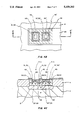
Referring to FIGS. 2A and 2B, the first embodiment of the present invention will be explained. An N-type epitaxial silicon layer 3 is formed on a P-type silicon body 1 and an N+ -type buried silicon layer 2 having an impurity concentration higher than the N-type epitaxial silicon layer 3 is provided between the silicon layer 3 and the silicon body 1. A thick field silicon oxide layer 4 is formed on the silicon body 1 and surrounds the epitaxial silicon layer 3 which is a transistor forming section. Further, the field silicon oxide layer 4 is contacted to peripheral sections of the buried layer 2. In the epitaxial transistor forming section 3, a trench 11 having a ring-like plan shape and a narrow width W2 of 0.2 μm to 0.5 μm is formed from the upper surface inwardly, and an insulating film 12 such as silicon nitride film fills the trench 11 completely. The ring-like trench 11 is represented by left-upward dotted lines hatching in FIG. 2A. A base region 17, which includes a P-type intrinsic base portion (active base portion) 37 and a P+ -type extrinsic base portion (graft base portion) 38 having an impurity concentration higher than the intrinsic base portion 37 and surrounding the intrinsic base portion, is formed inside the trench 11 such that the outer side of the extrinsic base portion 38 is entirely contacted to the trench 11, that is, to the insulating film 12 filling the trench and that a part of N-type conductivity type remains under the base region 17. The N-type part under the base region 17 and surrounded by the trench 11 is an active collector portion 33 of the collector region of the transistor and the N-type portion outside the trench 11 so as to surround the trench is a collector lead-out portion 34 of the collector region. The collector lead-out portion 34 may have an impurity concentration of N+ -type higher than the active collector portion 33. A collector electrode 5 of N-type polycrystalline silicon is contacted to the entire upper surface of the collector lead-out portion 34 and extends on the field silicon oxide layer 4. The collector lead-out portion 34 surrounds the active collector portion 33 via the trench 11, and therefore, the contact of the upper surface of the collector lead-out portion 34 and the collector electrode 5 also surrounds the active collector portion 33 in the plan view. The collector contact is represented by left-upward solid lines hatching in FIG. 2A. A base electrode 13 of P-type polycrystalline silicon is contacted to the graft base portion 38 and formed on upper parts of the insulating film 12 extending up from the trench 11 and on an insulating film 6 of silicon nitride film. The base contact is represented by right-upward solid lines hatching in FIG. 2A. An N+ -type emitter region 20 is formed in the P-type intrinsic base portion 37, and an emitter electrode 19 of N-type polycrystalline silicon is contacted to the emitter region 20 and formed on a thin oxide silicon film 16, on an insulating film 18 of silicon nitride film and on an insulating film 14 of silicon nitride film. An aluminum wiring 42 is connected to the collector electrode 5 through a contact hole 22 formed in the insulating films 6, 14, and also an aluminum wiring 41 is connected to the base electrode 13 through a contact hole 21 formed in the insulating film 14.
According to the present embodiment, the collector lead-out portion 34 surrounds the active collector portion 33 via the trench 11 and the collector electrode 5 is contacted to the entire upper surface of the collector lead-out portion. Further, the width W2 of the trench 11 is very narrow. Therefore, the collector resistance of the transistor is extremely reduced, and high operations of the transistor can be obtained.
Referring to FIGS. 3A to 3H, process steps for manufacturing the bipolar transistor shown in FIG. 2 will be explained.
First, as shown in FIG. 3A, an N+ -type buried layer 2 is provided on a principal surface of a P-type silicon body 1, and an N-type epitaxial layer 3 for forming a collector region is grown to a thickness of from 0.5 to 1.0 μm on the surface including the N+ -type buried layer 2. Next, a thick field silicon oxide layer 4 for element isolation, that is, transistor isolation is selectively formed by selective oxidation method to define a transistor forming section. Next, an N-type polycrystalline silicon layer 5 which is to become a collector electrode is deposited to a thickness of from 0.2 to 0.3 μm on the surface including the transistor forming section, and this layer is selectively etched to form a collector electrode which connects with the N-type epitaxial layer 3 in the transistor forming section. Next, a silicon nitride film 6 having a thickness of from 0.2 to 0.3 μm and a silicon oxide film 7 having a thickness of from 0.2 to 0.3 μm are successively deposited on the surface including the polycrystalline silicon layer 5.
Next, as shown in FIG. 3B, the silicon oxide film 7, the silicon nitride film 6 and the polycrystalline silicon film 5 are selectively removed successively by a lithography technique to form a first opening 8. Next, an oxidation-resistant silicon nitride film 9 is deposited to a thickness of from 0.2 to 0.5 μm on the surface including the opening 8.
Next, as shown in FIG. 3C, the whole surface is subjected to anisotropic etching by reactive ion etching (hereinafter referred to as "RIE") process to remove the silicon nitride film 9 except for those portions of the film 9 which are left on the vertical inner side surface of the opening 8, thereby exposing the surface of the N-type epitaxial layer 3 in the opening 8. The remaining silicon nitride film is the ring-plan shape side wall 9 having a width W3 ranging from 0.2 μm to 0.5 μm. Next, with the silicon oxide film 7 and the silicon nitride film (side wall) 9 used as masks, a silicon oxide film 10 having a thickness of from 0.1 to 0.2 μm is formed on the surface of the N-type epitaxial layer 3 in the opening 8 by thermal oxidation process.
Next, as shown in FIG. 3D, the silicon nitride film 9 is removed with hot phosphoric acid. At this time, the silicon nitride film 6 is not removed since its surface is covered with the silicon oxide film 7. Next, with the silicon oxide films 7 and 10 used as masks, a vertically extending deep trench with a width of 0.3 μm is formed in the surface of the N-type epitaxial layer 3 by RIE. Next, a silicon nitride film 12 having a thickness of from 0.3 to 0.4 μm is deposited on the surface including the trench 11 to fill the trench 11.
Next, as shown in FIG. 3E, the whole surface is subjected to anisotropic etching by RIE to remove the silicon nitride film 12 except for those of the film 12 which are left in the trench 11 and on the inner walls of the opening 8. Next, a P-type polycrystalline silicon layer 13 is deposited to a thickness of from 0.2 to 0.3 μm on the surface including the opening 8 and this silicon layer 13 is selectively etched to form a base electrode which connects with the N-type epitaxial layer 3 in the opening 8. Next, a silicon nitride film 14 is deposited on the surface including the polycrystalline silicon layer 13.
Next, as shown in FIG. 3F, the silicon nitride film 14 and the polycrystalline silicon layer 13 in the opening 8 are selectively etched successively to form a second opening 15 inside the opening 8, thereby exposing the surface of the N-type epitaxial layer 3. Next, a silicon oxide film 16 having a thickness of about 0.1 μm is formed on the exposed surface of the N-type epitaxial layer 3 and on the side surfaces of the polycrystalline silicon layer 13 by thermal oxidation process, and boron is introduced into the N-type epitaxial layer 3 by ion implantation under conditions of an accelerating energy of from 30 to 40 keV and a dosage amount on the order of from 1×10¹³ to 2×1013 cm-2 to form an intrinsic (active) base portion 37. Next, a silicon nitride film 18 is deposited to a thickness of 0.3 μm on the surface including the opening 15. Next, a heat treatment is carried out at 900° C. for 30 minutes to diffuse the boron contained in the P-type polycrystalline silicon layer 13 into the surface of the epitaxial layer 3, thereby forming an extrinsic (graft) base portion 38 which connects with the intrinsic base portion 37.
Next, as shown in FIG. 3G, the whole surface is subjected to anisotropic etching by RIE to remove the silicon nitride film 18 except for those portions of the film 18 which are left on the vertical inner side surface of the opening 15, thereby exposing the surface of the intrinsic base portion 37. Next, a non-doped polycrystalline silicon layer 19 is deposited on the surface including the opening 15. Next, arsenic is ion-implanted at a dosage of 1×1016 cm-2 and a heat treatment is carried out at 950° C. for 20 minutes to form an emitter region 20 in the intrinsic base portion 37.
Next, as shown in FIG. 3H, the polycrystalline silicon layer 19 is selectively removed by a photoetching technique to form an emitter electrode. Next, the silicon nitride film 14 is selectively etched to form a contact hole 21 for contact a wiring with the base electrode, and the silicon nitride films 14 and 6 are selectively etched successively to form a contact hole 22 for contact a wiring with the collector electrode, thus completing a bipolar transistor shown in FIG. 2.
It should be noted that, although the embodiment has been concerned an NPN-type bipolar transistor, the invention may similarly be applied to a PNP-type bipolar transistor. In such a case also, the same advantageous effects are obtained.
Referring to FIGS. 4A to 4C, a second embodiment of the present invention will be explained. FIG. 4A shows an ECL circuit connected between a ground line and an negative voltage power source line VEE and including first to fourth bipolar transistors Tr1 to Tr4, first to third resistors R1 to R3 and a constant current source I. First and second input signals IN1 and IN2 are sent to the bases of the first and second transistors, respectively, and a reference signal γef is sent to the base of the third transistor Tr3. The collectors of the first and second transistors are connected in common to each other and also the emitters of these transistors are connected in common to each other. Therefore, if the first and second transistors are formed in common in one element forming region of an epitaxial silicon layer surrounded by a field insulating layer, the integration density can be enhanced. However, in this case, an unfavorable parasitic lateral PNP action is apt to occur, and therefore, the common formation is difficult in a prior art.
According to the second embodiment of the present invention, however, the first and second transistors can be formed in one element forming region without occurring the parastic lateral PNP action, because each of the base regions and each of the active collector portions are surrounded by a trench of the present invention. Further, each of the trenches is in turn surrounded by a common collector lead-out portion to which a common collector electrode is connected at its entire upper surface. Therefore, the collector resistance of each transistor is reduced as in the first embodiment. Moreover, owing to the high integration density, the area of the common buried layer provided under the epitaxial element forming region can be small and the capacitance between the buried layer and the semiconductor body can be reduced. Consequently, operation speeds of the ECL device is further increased.
As shown in FIGS. 4B and 4C, the first transistor Tr1 including a P-type base region 56, an N+ -type emitter region 50 and an N- -type active collector portion 57 of a collector region and the second transistor Tr2 including a P-type base region 56', an N+ -type emitter region 50' and an N- -type active collector portion 57' of a collector region are formed in common in a common element forming region 3 of silicon epitaxial layer surrounded by a thick field silicon oxide layer 4 which is formed on a P-type silicon body 1. Between the epitaxial element forming region 3 and the silicon body 1, an N+ -type common buried layer 2 is formed. The base region 56 and the active collector portion 57 under the base region of the first transistor Tr1 is surrounded by a trench 51 filling with an insulating film 52, and base region 56' and the active collector portion 57' under the base region of the second transistor Tr2 is surrounded by a trench 51' filling with an insulating film 52'. The trench 51 forming the insulating film 52 therein and the trench 51' forming the insulating film 52' therein are represented by left-upward dotted lines hatching in FIG. 4B. Each of the trenches is surrounded by an N+ -type common collector lead-out portion 58 such that the portion 58 surrounds each of the active collector portions 57, 57'. A collector electrode 45 of N-type polycrystalline silicon is connected to the entire upper surface of the collector lead-out portion 58 and formed on the field silicon oxide layer 4. The collector contact is represented by left-upward solid lines hatching in FIG. 4B. Other components such as base and emitter electrodes, wirings, insulating films are omitted to show. However, they are the same as of the first embodiment shown in FIG. 2.

Claims (15)

What is claimed is:
1. A bipolar transistor comprising:
a semiconductor substrate having a major surface and a transistor forming section of a first conductivity type surrounded by a field insulating layer;
a trench formed in said transistor forming section from said major surface inwardly up to a first depth, said trench being closed upon itself in plan view and completely surrounding and encompassing a first portion of said transistor forming section and being completely surrounded and encompassed by a second portion of said transistor forming section which is positioned between said trench and said field insulating layer;
an insulating film filling said trench;
a first impurity region of a second conductivity type opposite to said first conductivity type formed in said first portion from said major surface up to a second depth shallower than said first depth such that a part of said first portion under said first impurity region remains as of said first conductivity type and that all side parts of said first impurity region are entirely contacted to said insulating film filling said trench;
a second impurity region of said first conductivity type formed at a center part of said first impurity region from said major surface up to a third depth shallower than said second depth;
a collector electrode entirely in contact with a contact part of said second portion of said transistor forming section between said trench and said field insulating layer, said contact part of said second portion having a closed shape encompassing and completely surrounding said trench and said part of said first portion under said first impurity region, in the plan view;
a base electrode entirely in contact with a periphery contact part of said first impurity region, said peripheral contact part having a closed shaped completely encompassing and surrounding said second impurity region and being completely encompassed and surrounded by said trench; and
an emitter electrode contacted to said second impurity region;
whereby, said part of said first portion under said first impurity region is an active collector portion of a collector of said transistor; said second portion is a collector lead-out portion of said collector; said first impurity region is a base of said transistor; and said second impurity region is an emitter of said transistor.
2. A bipolar transistor of claim 1, in which said trench has a width ranging from 0.2 μm to 0.5 μm.
3. A bipolar transistor of claim 1, in which said collector lead-out portion of said first conductivity type has an impurity concentration higher than that of said active collector portion of said first conductivity type.
4. A bipolar transistor of claim 1 further comprising a buried layer of said first conductivity type having an impurity concentration higher than that of said active collector portion and formed under said active collector portion.
5. A bipolar transistor of claim 4, in which said transistor forming section is constituted of an epitaxial silicon layer formed on said buried layer and above a silicon body, and said first depth of said trench is less than the thickness of said epitaxial silicon layer such that said trench is not reached to said buried layer.
6. A bipolar transistor of claim 1, in which said base includes an intrinsic base portion constituted of said center part of said first impurity region and an extrinsic base portion surrounding said intrinsic base portion and said peripheral contact part of said first impurity region is positioned at said extrinsic base portion.
7. A bipolar transistor of claim 1, in which said collector, base and emitter electrodes are made of polycrystalline silicon, respectively.
8. An integrated circuit semiconductor device comprising:
a semiconductor substrate having a major surface and a transistor forming section of a first conductivity type surrounded by a field insulating layer;
first and second trenches closed in plan view and being formed in said transistor forming section from said major surface inwardly up to a first depth, said first and second trenches completely encompassing and surrounding first and second portions of said transistor forming section, respectively and being completely encompassed and surrounded by a third portion of said transistor forming section positioned between said trenches and said field insulating layer and between said first and second trenches;
insulating films filling said first and second trenches, respectively;
first and second impurity regions of a second conductivity type opposite to said first conductivity type formed in said first and second portions, respectively, from said major surface up to a second depth shallower than said first depth such that parts of said first and second portions under said first and second impurity regions remain, respectively, as of said first conductivity type and that all of the side parts of said first and second impurity regions are entirely contacted to said insulating films filling said trenches, respectively;
third and fourth impurity regions of said first conductivity type formed at respective center parts of said first and second impurity regions from said major surface up to a third depth shallower than said second depth;
a common collector electrode entirely in contact with said major surface of said third portion of said transistor forming section such that the contact surrounds said first and second trenches and said parts of said first and second portions under said first and second impurity regions, in the plan view,
base electrodes contacted to respective periphery parts of said first and second impurity regions; and
emitter electrodes contacted to said third and fourth impurity regions, respectively;
whereby, said part of said first portion under said first impurity region is an active collector portion of a collector of a first bipolar transistor; said part of said second portion under said second impurity region is an active collector portion of a collector of a second bipolar transistor; said third portion is a common lead-out portion of said collectors of said first and second transistors; said first impurity region is a base of said first transistor; said second impurity region is a base of said second transistor; said third impurity region is an emitter of said first transistor; and said fourth impurity region is an emitter of said second transistor.
9. An integrated circuit semiconductor device of claim 8, in which said circuit is an ECL type logic circuit, and said first and second transistors are input transistors.
10. An integrated circuit semiconductor device of claim 9, in which said emitters of said first and second transistors are connected in common to each other.
11. An integrated circuit semiconductor device of claim 8, in which each of said trenches has a width ranging from 0.2 μm to 0.5 μm.
12. An integrated circuit semiconductor device of claim 8, in which said common collector lead-out portion of said first conductivity type has an impurity concentration higher than that of said active collector portions of said first conductivity type of said first and second transistors.
13. An integrated circuit semiconductor device of claim 8 further comprising a common buried layer of said first conductivity type having an impurity concentration higher than that of said active collector portions and formed under said active collector portions of said first and second transistors.
14. An integrated circuit semiconductor device of claim 13, in which said transistor forming section is constituted of an epitaxial silicon layer formed on said common buried layer and above a silicon body, and said first depth of said trenches is less than the thickness of said epitaxial silicon layer such that each of said trenches is not reached to said common buried layer.
15. An integrated circuit semiconductor device of claim 8, in which each of said bases includes an intrinsic base portion constituted of said center part of each of said first and second impurity regions and an extrinsic base portion surrounding said intrinsic base portion and constituted of said peripheral part of each of said first and second impurity regions.
US07/565,494 1988-06-27 1990-08-10 Bipolar transistor with reduced collector resistance Expired - Fee Related US5109262A (en)

Applications Claiming Priority (2)

Application Number Priority Date Filing Date Title
JP63159660A JPH027529A (en) 1988-06-27 1988-06-27 Bipolar transistor and its manufacture
JP63-159660 1988-06-27

Related Parent Applications (1)

Application Number Title Priority Date Filing Date
US07/372,424 Division US4980305A (en) 1988-06-27 1989-06-26 Method of manufacturing bipolar transistor

Publications (1)

Publication Number Publication Date
US5109262A true US5109262A (en) 1992-04-28

Family

ID=15698559

Family Applications (2)

Application Number Title Priority Date Filing Date
US07/372,424 Expired - Fee Related US4980305A (en) 1988-06-27 1989-06-26 Method of manufacturing bipolar transistor
US07/565,494 Expired - Fee Related US5109262A (en) 1988-06-27 1990-08-10 Bipolar transistor with reduced collector resistance

Family Applications Before (1)

Application Number Title Priority Date Filing Date
US07/372,424 Expired - Fee Related US4980305A (en) 1988-06-27 1989-06-26 Method of manufacturing bipolar transistor

Country Status (2)

Country Link
US (2) US4980305A (en)
JP (1) JPH027529A (en)

Cited By (18)

* Cited by examiner, † Cited by third party
Publication number Priority date Publication date Assignee Title
US5221857A (en) * 1990-12-19 1993-06-22 Nec Corporation Bipolar transistor structure with polycrystalline resistor layer
US5235206A (en) * 1990-10-24 1993-08-10 International Business Machines Corporation Vertical bipolar transistor with recessed epitaxially grown intrinsic base region
US5285101A (en) * 1990-08-28 1994-02-08 Nec Corporation Semiconductor device
US5324672A (en) * 1991-10-24 1994-06-28 Sony Corporation Manufacturing method for bipolar transistor
US5403757A (en) * 1992-08-31 1995-04-04 Nec Corporation Method of producing a double-polysilicon bipolar transistor
US5455448A (en) * 1992-09-03 1995-10-03 Sgs-Thomson Microelectronics, Inc. Bipolar, monolithic, high-power RF transistor with isolated top collector
US5465001A (en) * 1993-01-12 1995-11-07 France Telecom Electronic component capable of negative dynamic resistance
US5502330A (en) * 1995-02-23 1996-03-26 Texas Instruments Incorporated Stacked barrier-diffusion source and etch stop for double polysilicon BJT with patterned base link
US5512785A (en) * 1994-11-30 1996-04-30 Motorola, Inc. Semiconducter device having an emitter terminal separated from a base terminal by a composite nitride/oxide layer
US5528066A (en) * 1992-04-06 1996-06-18 Phoenix Vlsi Consultants Limited Bipolar transistor having a collector well with a particular concentration
US5608353A (en) * 1995-03-29 1997-03-04 Rf Micro Devices, Inc. HBT power amplifier
US5923584A (en) * 1995-02-17 1999-07-13 Micron Technology, Inc. Dual poly integrated circuit interconnect
US6110772A (en) * 1997-01-31 2000-08-29 Sanyo Electric Co., Ltd. Semiconductor integrated circuit and manufacturing method thereof
US6114744A (en) * 1997-03-14 2000-09-05 Sanyo Electric Company Semiconductor integration device and fabrication method of the same
US6784747B1 (en) 2003-03-20 2004-08-31 Analog Devices, Inc. Amplifier circuit
US6816015B2 (en) 2003-03-27 2004-11-09 Analog Devices, Inc. Amplifier circuit having a plurality of first and second base resistors
US9059138B2 (en) 2012-01-25 2015-06-16 International Business Machines Corporation Heterojunction bipolar transistor with reduced sub-collector length, method of manufacture and design structure
US20160204234A1 (en) * 2014-02-18 2016-07-14 International Business Machines Corporation Bipolar transistor with carbon alloyed contacts

Families Citing this family (11)

* Cited by examiner, † Cited by third party
Publication number Priority date Publication date Assignee Title
JP2641781B2 (en) * 1990-02-23 1997-08-20 シャープ株式会社 Method of forming semiconductor element isolation region
US5254485A (en) * 1990-09-18 1993-10-19 Matsushita Electric Industrial Co., Ltd. Method for manufacturing bipolar semiconductor device
US5391503A (en) * 1991-05-13 1995-02-21 Sony Corporation Method of forming a stacked semiconductor device wherein semiconductor layers and insulating films are sequentially stacked and forming openings through such films and etchings using one of the insulating films as a mask
JP2672199B2 (en) * 1991-05-21 1997-11-05 シャープ株式会社 Method for manufacturing semiconductor device
US5204277A (en) * 1992-02-03 1993-04-20 Motorola, Inc. Method of forming bipolar transistor having substrate to polysilicon extrinsic base contact
US5234846A (en) * 1992-04-30 1993-08-10 International Business Machines Corporation Method of making bipolar transistor with reduced topography
JP3343968B2 (en) * 1992-12-14 2002-11-11 ソニー株式会社 Bipolar semiconductor device and method of manufacturing the same
US5465006A (en) * 1994-07-15 1995-11-07 Hewlett-Packard Company Bipolar stripe transistor structure
KR100205017B1 (en) * 1995-12-20 1999-07-01 이계철 Method for manufacturing heterojunction bipolar transistor
SE1150065A1 (en) * 2011-01-31 2012-07-17 Fairchild Semiconductor Silicon carbide bipolar transistor with overgrown emitter
US20130277804A1 (en) * 2012-04-20 2013-10-24 International Business Machines Corporation Bipolar junction transistors with reduced base-collector junction capacitance

Citations (1)

* Cited by examiner, † Cited by third party
Publication number Priority date Publication date Assignee Title
US4745087A (en) * 1987-01-13 1988-05-17 Advanced Micro Devices, Inc. Method of making fully self-aligned bipolar transistor involving a polysilicon collector contact formed in a slot with an oxide sidewall

Family Cites Families (7)

* Cited by examiner, † Cited by third party
Publication number Priority date Publication date Assignee Title
JPS53132275A (en) * 1977-04-25 1978-11-17 Nippon Telegr & Teleph Corp <Ntt> Semiconductor device and its production
US4483726A (en) * 1981-06-30 1984-11-20 International Business Machines Corporation Double self-aligned fabrication process for making a bipolar transistor structure having a small polysilicon-to-extrinsic base contact area
JPS5946105B2 (en) * 1981-10-27 1984-11-10 日本電信電話株式会社 Bipolar transistor device and its manufacturing method
US4507171A (en) * 1982-08-06 1985-03-26 International Business Machines Corporation Method for contacting a narrow width PN junction region
JPH0658912B2 (en) * 1985-05-07 1994-08-03 日本電信電話株式会社 Bipolar transistor manufacturing method
JPS62141767A (en) * 1985-12-16 1987-06-25 Matsushita Electric Ind Co Ltd Semiconductor device and manufacture thereof
JPS6318673A (en) * 1986-07-11 1988-01-26 Yamaha Corp Manufacture of semiconductor device

Patent Citations (1)

* Cited by examiner, † Cited by third party
Publication number Priority date Publication date Assignee Title
US4745087A (en) * 1987-01-13 1988-05-17 Advanced Micro Devices, Inc. Method of making fully self-aligned bipolar transistor involving a polysilicon collector contact formed in a slot with an oxide sidewall

Cited By (20)

* Cited by examiner, † Cited by third party
Publication number Priority date Publication date Assignee Title
US5285101A (en) * 1990-08-28 1994-02-08 Nec Corporation Semiconductor device
US5235206A (en) * 1990-10-24 1993-08-10 International Business Machines Corporation Vertical bipolar transistor with recessed epitaxially grown intrinsic base region
US5221857A (en) * 1990-12-19 1993-06-22 Nec Corporation Bipolar transistor structure with polycrystalline resistor layer
US5324672A (en) * 1991-10-24 1994-06-28 Sony Corporation Manufacturing method for bipolar transistor
US5528066A (en) * 1992-04-06 1996-06-18 Phoenix Vlsi Consultants Limited Bipolar transistor having a collector well with a particular concentration
US5403757A (en) * 1992-08-31 1995-04-04 Nec Corporation Method of producing a double-polysilicon bipolar transistor
US5455448A (en) * 1992-09-03 1995-10-03 Sgs-Thomson Microelectronics, Inc. Bipolar, monolithic, high-power RF transistor with isolated top collector
US5465001A (en) * 1993-01-12 1995-11-07 France Telecom Electronic component capable of negative dynamic resistance
US5512785A (en) * 1994-11-30 1996-04-30 Motorola, Inc. Semiconducter device having an emitter terminal separated from a base terminal by a composite nitride/oxide layer
US5923584A (en) * 1995-02-17 1999-07-13 Micron Technology, Inc. Dual poly integrated circuit interconnect
US5502330A (en) * 1995-02-23 1996-03-26 Texas Instruments Incorporated Stacked barrier-diffusion source and etch stop for double polysilicon BJT with patterned base link
US5608353A (en) * 1995-03-29 1997-03-04 Rf Micro Devices, Inc. HBT power amplifier
US5629648A (en) * 1995-03-29 1997-05-13 Rf Micro Devices, Inc. HBT power amplifier
US6110772A (en) * 1997-01-31 2000-08-29 Sanyo Electric Co., Ltd. Semiconductor integrated circuit and manufacturing method thereof
US6114744A (en) * 1997-03-14 2000-09-05 Sanyo Electric Company Semiconductor integration device and fabrication method of the same
US6784747B1 (en) 2003-03-20 2004-08-31 Analog Devices, Inc. Amplifier circuit
US6816015B2 (en) 2003-03-27 2004-11-09 Analog Devices, Inc. Amplifier circuit having a plurality of first and second base resistors
US9059138B2 (en) 2012-01-25 2015-06-16 International Business Machines Corporation Heterojunction bipolar transistor with reduced sub-collector length, method of manufacture and design structure
US20160204234A1 (en) * 2014-02-18 2016-07-14 International Business Machines Corporation Bipolar transistor with carbon alloyed contacts
US9490352B2 (en) * 2014-02-18 2016-11-08 International Business Machines Corporation Bipolar transistor with carbon alloyed contacts

Also Published As

Publication number Publication date
US4980305A (en) 1990-12-25
JPH027529A (en) 1990-01-11

Similar Documents

Publication Publication Date Title
US5109262A (en) Bipolar transistor with reduced collector resistance
US4478655A (en) Method for manufacturing semiconductor device
US4089021A (en) Semiconductor device capable of withstanding high voltage and method of manufacturing same
US5323055A (en) Semiconductor device with buried conductor and interconnection layer
US4066473A (en) Method of fabricating high-gain transistors
US4115797A (en) Integrated injection logic with heavily doped injector base self-aligned with injector emitter and collector
US6573146B2 (en) Methods of manufacturing complementary bipolar transistors
US4963957A (en) Semiconductor device having bipolar transistor with trench
JPS6228577B2 (en)
US5108783A (en) Process for producing semiconductor devices
US4988639A (en) Method of manufacturing semiconductor devices using trench isolation method that forms highly flat buried insulation film
KR100270470B1 (en) Semiconductor device and method for fabricating the same
JPH0420265B2 (en)
JP2503733B2 (en) Method for manufacturing semiconductor device
US4566174A (en) Semiconductor device and method for manufacturing the same
EP0112489A1 (en) Semiconductor device with compact isolation and method of making the same
US5109263A (en) Semiconductor device with optimal distance between emitter and trench isolation
US5031020A (en) Semiconductor device having two different active elements whose partial area is commonly used
US3959039A (en) Method of manufacturing vertical complementary bipolar transistors each with epitaxial base zones
JP2809025B2 (en) Bipolar transistor
JP2940984B2 (en) Manufacturing method of BiCMOS type semiconductor integrated circuit
US5065210A (en) Lateral transistor structure for bipolar semiconductor integrated circuits
US4675983A (en) Method of making a semiconductor including forming graft/extrinsic and intrinsic base regions
JP3128818B2 (en) Semiconductor integrated circuit
JP2633374B2 (en) Semiconductor device and manufacturing method thereof

Legal Events

Date Code Title Description
FEPP Fee payment procedure

Free format text: PAYOR NUMBER ASSIGNED (ORIGINAL EVENT CODE: ASPN); ENTITY STATUS OF PATENT OWNER: LARGE ENTITY

FPAY Fee payment

Year of fee payment: 4

FEPP Fee payment procedure

Free format text: PAYER NUMBER DE-ASSIGNED (ORIGINAL EVENT CODE: RMPN); ENTITY STATUS OF PATENT OWNER: LARGE ENTITY

Free format text: PAYOR NUMBER ASSIGNED (ORIGINAL EVENT CODE: ASPN); ENTITY STATUS OF PATENT OWNER: LARGE ENTITY

FPAY Fee payment

Year of fee payment: 8

REMI Maintenance fee reminder mailed
LAPS Lapse for failure to pay maintenance fees
FP Lapsed due to failure to pay maintenance fee

Effective date: 20040428

STCH Information on status: patent discontinuation

Free format text: PATENT EXPIRED DUE TO NONPAYMENT OF MAINTENANCE FEES UNDER 37 CFR 1.362