US5115288A - Split-gate EPROM cell using polysilicon spacers - Google Patents
Split-gate EPROM cell using polysilicon spacers Download PDFInfo
- Publication number
- US5115288A US5115288A US07/728,823 US72882391A US5115288A US 5115288 A US5115288 A US 5115288A US 72882391 A US72882391 A US 72882391A US 5115288 A US5115288 A US 5115288A
- Authority
- US
- United States
- Prior art keywords
- floating gate
- gate
- region
- polysilicon
- edge
- Prior art date
- Legal status (The legal status is an assumption and is not a legal conclusion. Google has not performed a legal analysis and makes no representation as to the accuracy of the status listed.)
- Expired - Lifetime
Links
- 125000006850 spacer group Chemical group 0.000 title claims abstract description 36
- 229910021420 polycrystalline silicon Inorganic materials 0.000 title claims description 43
- 229920005591 polysilicon Polymers 0.000 title claims description 43
- 239000011810 insulating material Substances 0.000 claims description 11
- 239000000758 substrate Substances 0.000 claims description 8
- 229910052710 silicon Inorganic materials 0.000 claims description 3
- 239000010703 silicon Substances 0.000 claims description 3
- 239000004065 semiconductor Substances 0.000 claims description 2
- 239000012212 insulator Substances 0.000 claims 1
- 238000000034 method Methods 0.000 abstract description 8
- 238000005516 engineering process Methods 0.000 abstract description 3
- 238000004519 manufacturing process Methods 0.000 abstract 1
- 210000004027 cell Anatomy 0.000 description 42
- 239000007943 implant Substances 0.000 description 4
- 229910052785 arsenic Inorganic materials 0.000 description 2
- RQNWIZPPADIBDY-UHFFFAOYSA-N arsenic atom Chemical compound [As] RQNWIZPPADIBDY-UHFFFAOYSA-N 0.000 description 2
- 238000005530 etching Methods 0.000 description 2
- 230000000873 masking effect Effects 0.000 description 2
- 229920002120 photoresistant polymer Polymers 0.000 description 2
- XUIMIQQOPSSXEZ-UHFFFAOYSA-N Silicon Chemical compound [Si] XUIMIQQOPSSXEZ-UHFFFAOYSA-N 0.000 description 1
- 210000001744 T-lymphocyte Anatomy 0.000 description 1
- 230000015572 biosynthetic process Effects 0.000 description 1
- 230000001419 dependent effect Effects 0.000 description 1
- 238000009792 diffusion process Methods 0.000 description 1
- 229910052751 metal Inorganic materials 0.000 description 1
- 239000002184 metal Substances 0.000 description 1
- 238000012856 packing Methods 0.000 description 1
- 230000000750 progressive effect Effects 0.000 description 1
- 238000010405 reoxidation reaction Methods 0.000 description 1
Images


Classifications
-
- H—ELECTRICITY
- H01—ELECTRIC ELEMENTS
- H01L—SEMICONDUCTOR DEVICES NOT COVERED BY CLASS H10
- H01L29/00—Semiconductor devices adapted for rectifying, amplifying, oscillating or switching, or capacitors or resistors with at least one potential-jump barrier or surface barrier, e.g. PN junction depletion layer or carrier concentration layer; Details of semiconductor bodies or of electrodes thereof ; Multistep manufacturing processes therefor
- H01L29/66—Types of semiconductor device ; Multistep manufacturing processes therefor
- H01L29/68—Types of semiconductor device ; Multistep manufacturing processes therefor controllable by only the electric current supplied, or only the electric potential applied, to an electrode which does not carry the current to be rectified, amplified or switched
- H01L29/76—Unipolar devices, e.g. field effect transistors
- H01L29/772—Field effect transistors
- H01L29/78—Field effect transistors with field effect produced by an insulated gate
- H01L29/788—Field effect transistors with field effect produced by an insulated gate with floating gate
- H01L29/7881—Programmable transistors with only two possible levels of programmation
-
- H—ELECTRICITY
- H01—ELECTRIC ELEMENTS
- H01L—SEMICONDUCTOR DEVICES NOT COVERED BY CLASS H10
- H01L21/00—Processes or apparatus adapted for the manufacture or treatment of semiconductor or solid state devices or of parts thereof
- H01L21/02—Manufacture or treatment of semiconductor devices or of parts thereof
- H01L21/04—Manufacture or treatment of semiconductor devices or of parts thereof the devices having at least one potential-jump barrier or surface barrier, e.g. PN junction, depletion layer or carrier concentration layer
- H01L21/18—Manufacture or treatment of semiconductor devices or of parts thereof the devices having at least one potential-jump barrier or surface barrier, e.g. PN junction, depletion layer or carrier concentration layer the devices having semiconductor bodies comprising elements of Group IV of the Periodic System or AIIIBV compounds with or without impurities, e.g. doping materials
- H01L21/28—Manufacture of electrodes on semiconductor bodies using processes or apparatus not provided for in groups H01L21/20 - H01L21/268
- H01L21/28008—Making conductor-insulator-semiconductor electrodes
- H01L21/28017—Making conductor-insulator-semiconductor electrodes the insulator being formed after the semiconductor body, the semiconductor being silicon
- H01L21/28026—Making conductor-insulator-semiconductor electrodes the insulator being formed after the semiconductor body, the semiconductor being silicon characterised by the conductor
- H01L21/28123—Lithography-related aspects, e.g. sub-lithography lengths; Isolation-related aspects, e.g. to solve problems arising at the crossing with the side of the device isolation; Planarisation aspects
- H01L21/2815—Lithography-related aspects, e.g. sub-lithography lengths; Isolation-related aspects, e.g. to solve problems arising at the crossing with the side of the device isolation; Planarisation aspects part or whole of the electrode is a sidewall spacer or made by a similar technique, e.g. transformation under mask, plating
-
- H—ELECTRICITY
- H01—ELECTRIC ELEMENTS
- H01L—SEMICONDUCTOR DEVICES NOT COVERED BY CLASS H10
- H01L29/00—Semiconductor devices adapted for rectifying, amplifying, oscillating or switching, or capacitors or resistors with at least one potential-jump barrier or surface barrier, e.g. PN junction depletion layer or carrier concentration layer; Details of semiconductor bodies or of electrodes thereof ; Multistep manufacturing processes therefor
- H01L29/40—Electrodes ; Multistep manufacturing processes therefor
- H01L29/401—Multistep manufacturing processes
- H01L29/4011—Multistep manufacturing processes for data storage electrodes
- H01L29/40114—Multistep manufacturing processes for data storage electrodes the electrodes comprising a conductor-insulator-conductor-insulator-semiconductor structure
-
- Y—GENERAL TAGGING OF NEW TECHNOLOGICAL DEVELOPMENTS; GENERAL TAGGING OF CROSS-SECTIONAL TECHNOLOGIES SPANNING OVER SEVERAL SECTIONS OF THE IPC; TECHNICAL SUBJECTS COVERED BY FORMER USPC CROSS-REFERENCE ART COLLECTIONS [XRACs] AND DIGESTS
- Y10—TECHNICAL SUBJECTS COVERED BY FORMER USPC
- Y10S—TECHNICAL SUBJECTS COVERED BY FORMER USPC CROSS-REFERENCE ART COLLECTIONS [XRACs] AND DIGESTS
- Y10S257/00—Active solid-state devices, e.g. transistors, solid-state diodes
- Y10S257/90—MOSFET type gate sidewall insulating spacer
Definitions
- the present invention relates to split-gate memory cells of the type utilizable in an erasable programmable read only memory (EPROM) and, more particularly, to a split-gate memory cell that utilizes a polysilicon spacer to define the gate length of the series select transistor in a virtual-ground split-gate EPROM cell. Since the length of the polysilicon spacer can be controlled with great precision, misalignment problems associated with prior art split-gate cells are eliminated, thereby reducing cell size.
- EPROM erasable programmable read only memory
- Virtual-ground split-gate EPROM cells have been proposed as a means for improving on the packing density and yield of conventional "T" EPROM cells. These cells offer two key features. First, the use of buried N+ bits lines drastically reduces the number of contacts needed in the memory array. This confers an immediate yield advantage, since metal coverage of contact topology is a significant cause of yield loss in scaled integrated circuit technologies. By sharing bit line contacts among a large number of cells, the layout area associated with each cell is further reduced. Second, providing a series select transistor associated with each floating gate insures that the cell cannot be inadvertently turned on due to voltage coupled from the drain to the floating gate. This significantly relieves the constraints on drain programming voltage experienced with a convention T-cell EPROM.
- associating a series select transistor with each floating-gate confers asymmetry to the operation of the cell. If the source and drain terminals of the cell are interchanged, no programming can take place. This considerably simplifies the programming decoding of the array, since the cell next to the one being programmed is inherently resistant to programming: it cannot be disturbed by the high voltage applied to its source node, which also serves as the drain node of the programmed cell.
- FIG. 1A The cells differ only in the way in which they are arrayed.
- the Eitan array is illustrated in FIG. 1B.
- the Ali et al array is illustrated in FIG. 1C.
- the length of the series select transistor is defined by the masking of the buried N+ layer. This creates several problems. First, the length of the series select transistor and, hence, the electrical characteristics of the cell, are dependent upon the alignment of the buried N+ region to the polysilicon floating gate. This introduces significant variation in cell performance from die to die and from wafer to wafer. Second, the uncertainty in the final position of the buried N+ region causes variation in the series resistance of the buried bit line, causing further variation in cell performance.
- the width of the buried N+ bit line must be drawn wider than the required minimum. This increases the overall area of the cell.
- the present invention provides a split-gate EPROM cell that uses a polysilicon spacer to define the gate length of the series select transistor.
- the length of the polysilicon spacer can be controlled with great precision using existing integrated circuit process technologies and, therefore, can eliminate the misalignment problems associated with the prior art split-gate cells.
- a floating gate is formed on a layer of insulating material overlying a semiconductor substrate.
- a second layer of insulating material is then formed on the floating gate.
- Opposing sides of the floating gate are then sealed with insulating material.
- a conductive spacer is formed adjacent to one of the opposing sides of the floating gate. The conductive spacer is insulated from the floating gate by the seal and from the substrate by the first layer of insulating material.
- the spacer is utilized to define a self-aligned source region while the floating gate is utilized in the self-aligned definition of the drain region.
- This process results in the floating gate extending only over a portion of the channel region in the manner of a convention split-gate cell, and with the spacer being positioned over the remaining portion of the channel between the floating gate and the source region.
- a conductive control gate is then formed in electrical contact with the conductive spacer.
- the control gate also extends over the floating gate, but is electrically insulated from the floating gate by the second layer of insulating material.
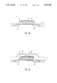
- FIG. 1A is a cross-sectional view illustrating a conventional virtual-ground split-gate EPROM cell.
- FIG. 1B is a simple schematic illustration of a virtual-ground EPROM array configuration.
- FIG. 1C is a simple schematic illustrating a staggered virtual-ground EPROM array configuration.
- FIGS. 2A-2E are cross-sectional views providing progressive illustration of a method of forming a split-gate memory cell in accordance with the present invention.
- FIGS. 3A and 3B are cross-sectional views illustrating alternative steps utilizable in forming a split-gate memory cell in accordance with the present invention.
- FIG. 4 is plan view of a split-gate memory cell in accordance with the present invention in a virtual-ground configuration.
- FIG. 5 is a plan view of a split-gate memory cell in accordance with the present invention in a staggered virtual-ground configuration.
- FIGS. 2A-2E show a sequence utilizable for fabricating a split-gate memory cell in accordance with the present invention.
- a layer of first polysilicon has been deposited on gate oxide and then doped in the conventional manner.
- ONO oxide-nitride-oxide
- the ONO/polysilicon layers are patterned and etched to define a polysilicon floating gate 10. This etching process typically also results in the etching of a portion of the gate oxide layer.
- a reoxidation is then been performed to seal the sides of the polysilicon gate 10 with sidewall oxide and to regrow the gate oxide to form gate oxide layer 14.
- a layer of second polysilicon (approximately 2000-3000 Angstroms thick) has been deposited and doped and an anisotropic etch performed to leave well-defined polysilicon spacers 16,18 along the opposing edges of the polysilicon floating gate 10.
- the source side S of the structure is then masked with photoresist 20 and the polysilicon spacer 18 on the drain side D is etched away using a selective silicon etch.
- a self-aligned arsenic N+ implant is then performed to form source region 22 and drain region 24. That is, on the source side S, the inner edge of the source region 22 is defined by the outer edge of the polysilicon spacer 16. Similarly, on the drain side D, the inner edge of the drain region 24 is defined by the edge of the polysilicon floating gate 10.
- junction depth of the arsenic implant is chosen such that the buried N+ drain region 24 underlaps the polysilicon floating gate 10 on the drain side D and such that the buried N+ source region 22 underlaps the polysilicon spacer 16 on the source side S, but does not reach all the way across to the polysilicon floating gate 10. In this way, a gated channel region is formed under the polysilicon spacer 16 on the source side S.
- a layer of third polysilicon 26 is then deposited and doped. This third polysilicon layer 26 is then masked and etched to form the control gate of the cell. Since the third polysilicon layer 26 is an intimate contact with the polysilicon spacer 16, a direct electrical connection is formed between them. In this way, the final cell structure, shown in FIG. 2E, is electrically equivalent to the conventional virtual-ground EPROM cell shown in FIG. 1A.
- FIG. 2E The significant advantage of the structure shown in FIG. 2E is that the channel length of the series transistor is defined by the width of the polysilicon spacer 16 and by the lateral diffusion of the buried N+ source region 22, both of which are parameters that can be very tightly controlled. Therefore, the FIG. 2E structure is much more alignment insensitive then are prior art split-gate EPROM cell structures and, thus, can be laid out in smaller areas and show much less variation in electrical performance.
- the need to etch the polysilicon spacer 18 (FIG. 2B) away from the drain side D of the polysilicon floating gate 10 can be eliminated.
- processing follows the previous flow to FIG. 2A.
- a photoresist masking layer 28 is applied to protect the source side S of the structure and an initial self-aligned N+ implant is performed to form buried N+ drain region 24'.
- Polysilicon spacers 16' and 18' are then formed as discussed above with respect to FIG. 2B.
- the spacer removal step described with respect to FIG. 2C can now be eliminated, since the early buried N+ implant forms a conducting layer under the polysilicon spacer 18' on the drain side D. Processing then continues as previously described, arriving at the final structure shown in FIG. 3B.
- FIG. 4 shows a plan view of the cell, laid out to correspond topologically with the prior art array shown in FIG. 1B.
- a plan view of the cell with a staggered layout corresponding to that shown in prior art FIG. 1C is shown in FIG. 5.
Abstract
The present invention provides an integrated circuit fabrication method that utilizes a conductive spacer to define the gate length of the series select transistor in a split-gate memory cell. Since the length of the spacer can be controlled with great precision using existing integrated circuit process technologies, misalignment problems associated with the prior art split-gate cells are eliminated.
Description
This is a continuation of co-pending application Ser. No. 545,397 filed on Jun. 28, 1990, now abandoned.
1. Field of the Invention
The present invention relates to split-gate memory cells of the type utilizable in an erasable programmable read only memory (EPROM) and, more particularly, to a split-gate memory cell that utilizes a polysilicon spacer to define the gate length of the series select transistor in a virtual-ground split-gate EPROM cell. Since the length of the polysilicon spacer can be controlled with great precision, misalignment problems associated with prior art split-gate cells are eliminated, thereby reducing cell size.
2. Discussion of the Prior Art
Virtual-ground split-gate EPROM cells have been proposed as a means for improving on the packing density and yield of conventional "T" EPROM cells. These cells offer two key features. First, the use of buried N+ bits lines drastically reduces the number of contacts needed in the memory array. This confers an immediate yield advantage, since metal coverage of contact topology is a significant cause of yield loss in scaled integrated circuit technologies. By sharing bit line contacts among a large number of cells, the layout area associated with each cell is further reduced. Second, providing a series select transistor associated with each floating gate insures that the cell cannot be inadvertently turned on due to voltage coupled from the drain to the floating gate. This significantly relieves the constraints on drain programming voltage experienced with a convention T-cell EPROM. Furthermore, associating a series select transistor with each floating-gate confers asymmetry to the operation of the cell. If the source and drain terminals of the cell are interchanged, no programming can take place. This considerably simplifies the programming decoding of the array, since the cell next to the one being programmed is inherently resistant to programming: it cannot be disturbed by the high voltage applied to its source node, which also serves as the drain node of the programmed cell.
U.S. Pat. No. 4,639,893 issued Jan. 27, 1987 to Boaz Eitan discloses an implementation of a virtual-ground split-gate EPROM cell. A second split-gate cell implementation has been reported by Ali et al., "A new Staggered Virtual-Ground array architecture implemented in a 4Mb CMOS EPROM", 1989 VLSI Circuits Conference, Tokyo, Japan.
These two implementations of a split-gate cell have the same cross-section, which is shown in FIG. 1A. The cells differ only in the way in which they are arrayed. The Eitan array is illustrated in FIG. 1B. The Ali et al array is illustrated in FIG. 1C.
Both of these cells suffer from the same major problem. That is, the length of the series select transistor is defined by the masking of the buried N+ layer. This creates several problems. First, the length of the series select transistor and, hence, the electrical characteristics of the cell, are dependent upon the alignment of the buried N+ region to the polysilicon floating gate. This introduces significant variation in cell performance from die to die and from wafer to wafer. Second, the uncertainty in the final position of the buried N+ region causes variation in the series resistance of the buried bit line, causing further variation in cell performance. Third, in order to insure that the resistance of the buried N+ bit line is acceptably low, under worse-case misalignment of the buried N+ region, the width of the buried N+ bit line must be drawn wider than the required minimum. This increases the overall area of the cell.
The present invention provides a split-gate EPROM cell that uses a polysilicon spacer to define the gate length of the series select transistor. The length of the polysilicon spacer can be controlled with great precision using existing integrated circuit process technologies and, therefore, can eliminate the misalignment problems associated with the prior art split-gate cells.
To fabricate a split-gate memory cell in accordance with the present invention, a floating gate is formed on a layer of insulating material overlying a semiconductor substrate. A second layer of insulating material is then formed on the floating gate. Opposing sides of the floating gate are then sealed with insulating material. Next, a conductive spacer is formed adjacent to one of the opposing sides of the floating gate. The conductive spacer is insulated from the floating gate by the seal and from the substrate by the first layer of insulating material. Next, the spacer is utilized to define a self-aligned source region while the floating gate is utilized in the self-aligned definition of the drain region. This process results in the floating gate extending only over a portion of the channel region in the manner of a convention split-gate cell, and with the spacer being positioned over the remaining portion of the channel between the floating gate and the source region. A conductive control gate is then formed in electrical contact with the conductive spacer. The control gate also extends over the floating gate, but is electrically insulated from the floating gate by the second layer of insulating material.
A better understanding of the features and advantages of the present will be obtained by reference to the following detailed description of the invention and accompanying drawings which set forth illustrative embodiments in which the principals of the invention are utilized.
FIG. 1A is a cross-sectional view illustrating a conventional virtual-ground split-gate EPROM cell.
FIG. 1B is a simple schematic illustration of a virtual-ground EPROM array configuration.
FIG. 1C is a simple schematic illustrating a staggered virtual-ground EPROM array configuration.
FIGS. 2A-2E are cross-sectional views providing progressive illustration of a method of forming a split-gate memory cell in accordance with the present invention.
FIGS. 3A and 3B are cross-sectional views illustrating alternative steps utilizable in forming a split-gate memory cell in accordance with the present invention.
FIG. 4 is plan view of a split-gate memory cell in accordance with the present invention in a virtual-ground configuration.
FIG. 5 is a plan view of a split-gate memory cell in accordance with the present invention in a staggered virtual-ground configuration.
FIGS. 2A-2E show a sequence utilizable for fabricating a split-gate memory cell in accordance with the present invention.
In FIG. 2A, a layer of first polysilicon has been deposited on gate oxide and then doped in the conventional manner. Following conventional formation of an oxide-nitride-oxide (ONO) layer 12, the ONO/polysilicon layers are patterned and etched to define a polysilicon floating gate 10. This etching process typically also results in the etching of a portion of the gate oxide layer. A reoxidation is then been performed to seal the sides of the polysilicon gate 10 with sidewall oxide and to regrow the gate oxide to form gate oxide layer 14.
Next, as shown in FIG. 2B, and in accordance with the present invention, a layer of second polysilicon (approximately 2000-3000 Angstroms thick) has been deposited and doped and an anisotropic etch performed to leave well-defined polysilicon spacers 16,18 along the opposing edges of the polysilicon floating gate 10.
As shown in FIG. 2C, the source side S of the structure is then masked with photoresist 20 and the polysilicon spacer 18 on the drain side D is etched away using a selective silicon etch.
As shown in FIG. 2D, a self-aligned arsenic N+ implant is then performed to form source region 22 and drain region 24. That is, on the source side S, the inner edge of the source region 22 is defined by the outer edge of the polysilicon spacer 16. Similarly, on the drain side D, the inner edge of the drain region 24 is defined by the edge of the polysilicon floating gate 10.
The junction depth of the arsenic implant is chosen such that the buried N+ drain region 24 underlaps the polysilicon floating gate 10 on the drain side D and such that the buried N+ source region 22 underlaps the polysilicon spacer 16 on the source side S, but does not reach all the way across to the polysilicon floating gate 10. In this way, a gated channel region is formed under the polysilicon spacer 16 on the source side S.
As shown in FIG. 2E, a layer of third polysilicon 26 is then deposited and doped. This third polysilicon layer 26 is then masked and etched to form the control gate of the cell. Since the third polysilicon layer 26 is an intimate contact with the polysilicon spacer 16, a direct electrical connection is formed between them. In this way, the final cell structure, shown in FIG. 2E, is electrically equivalent to the conventional virtual-ground EPROM cell shown in FIG. 1A.
The significant advantage of the structure shown in FIG. 2E is that the channel length of the series transistor is defined by the width of the polysilicon spacer 16 and by the lateral diffusion of the buried N+ source region 22, both of which are parameters that can be very tightly controlled. Therefore, the FIG. 2E structure is much more alignment insensitive then are prior art split-gate EPROM cell structures and, thus, can be laid out in smaller areas and show much less variation in electrical performance.
Variances on the basic process and structure described above may be utilized in practicing the present invention, but all retain the central concept of using a polysilicon spacer to define the channel length of the series transistor in a split-gate memory cell.
In accordance with an alternative and preferred embodiment of the invention, the need to etch the polysilicon spacer 18 (FIG. 2B) away from the drain side D of the polysilicon floating gate 10 can be eliminated. In this case, processing follows the previous flow to FIG. 2A. Referring to FIG. 3A, at this point, a photoresist masking layer 28 is applied to protect the source side S of the structure and an initial self-aligned N+ implant is performed to form buried N+ drain region 24'. Polysilicon spacers 16' and 18' are then formed as discussed above with respect to FIG. 2B. However, the spacer removal step described with respect to FIG. 2C can now be eliminated, since the early buried N+ implant forms a conducting layer under the polysilicon spacer 18' on the drain side D. Processing then continues as previously described, arriving at the final structure shown in FIG. 3B.
In the foregoing description of the invention, only the cell cross-section has been discussed. FIG. 4 shows a plan view of the cell, laid out to correspond topologically with the prior art array shown in FIG. 1B. A plan view of the cell with a staggered layout corresponding to that shown in prior art FIG. 1C is shown in FIG. 5.
It should be understood that various alternatives to the embodiments of the invention described herein may be employed in practicing the invention. It is intended that the following claims defined the scope of the invention and that structures and methods within the scope of these claims and their equivalents be covered thereby.
Claims (4)
1. A split-gate memory cell utilizable in a virtual ground erasable programmable read only memory array, the memory cell comprising:
(a) a semiconductor substrate of a first conductivity type having first and second spaced-apart regions of a second conductivity type formed therein, the first and second regions defining a substrate channel region therebetween;
(b) a first layer of insulating material formed on the channel region;
(c) a conductive floating gate formed on the insulating material and extending over a first section of the channel region between a first edge of the floating gate and the first region, thereby defining a second section of the channel region between the first edge of the floating gate and the second region, a second edge of the floating gate being used to define an edge of the first region;
(d) a second layer of insulating material formed on the floating gate;
(e) a conductive spacer formed adjacent to the floating gate and overlying the second section of the channel region, the conductive spacer being insulated from the floating gate by sidewall insulator formed therebetween, the conductive spacer being used to define an edge of the second region; and
(f) a conductive control gate formed subsequent to and in electrical contact with the conductive spacer and overlying but electrically insulated from the floating gate by the second layer of insulating material, the control gate extending in a direction parallel to the direction of current flow between the first and second regions.
2. A split-gate memory cell utilizable in a virtual ground erasable programmable read only memory array, the memory cell comprising:
(a) a P- silicon substrate having first and second spaced-apart N+ regions formed therein and defining a substrate channel region therebetween;
(b) a layer of gate oxide formed on the channel region;
(c) a polysilicon floating gate formed on the gate oxide and extending over a first section of the channel region between a first edge of the floating gate and the first N+ region, thereby defining a second section of the channel region between the first edge of the floating gate and the second N+ region, a second edge of the floating gate being used to define an edge of the first N+ region;
(d) a polysilicon spacer formed adjacent to the floating gate and overlying the second section of the channel region, the polysilicon spacer being insulated from the floating gate by sidewall oxide formed therebetween, the polysilicon spacer being used to define an edge of the second N+ region; and
(e) a polysilicon control gate formed subsequent to and in electrical contact with the conductive spacer and overlying but electrically insulated from the floating gate by a layer of insulating material formed therebetween, the control gate extending in a direction parallel to the direction of current flow between the first and second N+ regions.
3. A split-gate memory cell as in claim 2 wherein the layer of insulating material formed between the polysilicon control gate and the floating gate is an oxide-nitride-oxide layer.
4. A split-gate memory cell utilizable in a virtual ground erasable programmable read only memory array, the memory cell comprising:
(a) a P- silicon substrate having first and second spaced-apart N+ regions formed therein and defining a substrate channel region therebetween;
(b) a layer of gate oxide formed on the channel region;
(c) a polysilicon floating gate formed on the gate oxide and extending over a first section of the channel region between a first edge of the floating gate and the first N+ region, thereby defining a second section of the channel region between the first edge of the floating gate and the second N+ region, a second edge of the floating gate being used to define an edge of the first N+ region;
(d) first and second polysilicon spacers formed adjacent to the first and second edges of the polysilicon floating gate, respectively, the first polysilicon spacer overlying the first N+ region and insulated from the floating gate by sidewall oxide formed therebetween, the second polysilicon spacer overlying the second section of the channel region, and insulated from the floating gate by sidewall oxide formed therebetween;
(e) a polysilicon control gate formed subsequent to and in electrical contact with the first and second polysilicon spacers and overlying but electrically insulated from the floating gate by a layer of ONO formed therebetween, the control gate extending in a direction parallel to the direction of current flow between the first and second N+ regions.
Priority Applications (1)
| Application Number | Priority Date | Filing Date | Title |
|---|---|---|---|
| US07/728,823 US5115288A (en) | 1990-06-28 | 1991-07-09 | Split-gate EPROM cell using polysilicon spacers |
Applications Claiming Priority (2)
| Application Number | Priority Date | Filing Date | Title |
|---|---|---|---|
| US54539790A | 1990-06-28 | 1990-06-28 | |
| US07/728,823 US5115288A (en) | 1990-06-28 | 1991-07-09 | Split-gate EPROM cell using polysilicon spacers |
Related Parent Applications (1)
| Application Number | Title | Priority Date | Filing Date |
|---|---|---|---|
| US54539790A Continuation | 1990-06-28 | 1990-06-28 |
Publications (1)
| Publication Number | Publication Date |
|---|---|
| US5115288A true US5115288A (en) | 1992-05-19 |
Family
ID=27067923
Family Applications (1)
| Application Number | Title | Priority Date | Filing Date |
|---|---|---|---|
| US07/728,823 Expired - Lifetime US5115288A (en) | 1990-06-28 | 1991-07-09 | Split-gate EPROM cell using polysilicon spacers |
Country Status (1)
| Country | Link |
|---|---|
| US (1) | US5115288A (en) |
Cited By (32)
| Publication number | Priority date | Publication date | Assignee | Title |
|---|---|---|---|---|
| US5166902A (en) * | 1991-03-18 | 1992-11-24 | United Technologies Corporation | SRAM memory cell |
| US5262655A (en) * | 1991-04-23 | 1993-11-16 | Mitsubishi Denki Kabushiki Kaisha | Thin film field effect device having an LDD structure and a method of manufacturing such a device |
| US5274588A (en) * | 1991-07-25 | 1993-12-28 | Texas Instruments Incorporated | Split-gate cell for an EEPROM |
| US5414287A (en) * | 1994-04-25 | 1995-05-09 | United Microelectronics Corporation | Process for high density split-gate memory cell for flash or EPROM |
| US5508955A (en) * | 1993-05-20 | 1996-04-16 | Nexcom Technology, Inc. | Electronically erasable-programmable memory cell having buried bit line |
| US5541876A (en) * | 1994-06-01 | 1996-07-30 | United Microelectronics Corporation | Memory cell fabricated by floating gate structure |
| US5557569A (en) * | 1993-10-12 | 1996-09-17 | Texas Instruments Incorporated | Low voltage flash EEPROM C-cell using fowler-nordheim tunneling |
| US5627091A (en) * | 1994-06-01 | 1997-05-06 | United Microelectronics Corporation | Mask ROM process for making a ROM with a trench shaped channel |
| US5633185A (en) * | 1992-01-22 | 1997-05-27 | Macronix International Co., Ltd. | Method of making a non-volatile memory cell |
| US5667632A (en) * | 1995-11-13 | 1997-09-16 | Motorola, Inc. | Method of defining a line width |
| US5703387A (en) * | 1994-09-30 | 1997-12-30 | United Microelectronics Corp. | Split gate memory cell with vertical floating gate |
| US5714786A (en) * | 1996-10-31 | 1998-02-03 | Micron Technology, Inc. | Transistors having controlled conductive spacers, uses of such transistors and methods of making such transistors |
| US5841700A (en) * | 1992-09-08 | 1998-11-24 | National Semiconductor Corporation | Source-coupling, split gate, virtual ground flash EEPROM array |
| US5882973A (en) * | 1997-01-27 | 1999-03-16 | Advanced Micro Devices, Inc. | Method for forming an integrated circuit having transistors of dissimilarly graded junction profiles |
| US5900657A (en) * | 1997-05-19 | 1999-05-04 | National Semiconductor Corp. | MOS switch that reduces clock feed through in a switched capacitor circuit |
| US5910912A (en) * | 1992-10-30 | 1999-06-08 | International Business Machines Corporation | Flash EEPROM with dual-sidewall gate |
| US5939791A (en) * | 1995-12-27 | 1999-08-17 | Vlsi Technology, Inc. | Electrically conductive interconnects for integrated circuits |
| US5994239A (en) * | 1997-12-18 | 1999-11-30 | Advanced Micro Devices, Inc. | Manufacturing process to eliminate polystringers in high density nand-type flash memory devices |
| US6001690A (en) * | 1998-02-13 | 1999-12-14 | Taiwan Semiconductor Manufacturing Company, Ltd. | Method of forming flash EPROM by using iso+aniso silicon nitride spacer etching technology |
| US6063668A (en) * | 1997-12-18 | 2000-05-16 | Advanced Micro Devices, Inc. | Poly I spacer manufacturing process to eliminate polystringers in high density nand-type flash memory devices |
| US6069042A (en) * | 1998-02-13 | 2000-05-30 | Taiwan Semiconductor Manufacturing Company | Multi-layer spacer technology for flash EEPROM |
| US6117728A (en) * | 1995-05-19 | 2000-09-12 | Micron Technology, Inc. | Programmable non-volatile memory cell and method of forming a non-volatile memory cell |
| US6159829A (en) * | 1996-09-16 | 2000-12-12 | Warren; William L. | Memory device using movement of protons |
| US6252271B1 (en) | 1998-06-15 | 2001-06-26 | International Business Machines Corporation | Flash memory structure using sidewall floating gate and method for forming the same |
| US6281078B1 (en) * | 1997-12-18 | 2001-08-28 | Advanced Micro Devices, Inc. | Manufacturing process to eliminate ONO fence material in high density NAND-type flash memory devices |
| US6323086B2 (en) * | 1998-06-15 | 2001-11-27 | International Business Machines Corporation | Flash memory structure using sidewall floating gate having one side thereof surrounded by control gate |
| US20040196720A1 (en) * | 2003-03-11 | 2004-10-07 | Chih-Wei Hung | [flash memory with self-aligned split gate and methods for fabricating and for operating the same] |
| US20050036353A1 (en) * | 2003-07-09 | 2005-02-17 | Kikuko Sugimae | Nonvolatile semiconductor memory device |
| US20060189073A1 (en) * | 2005-02-22 | 2006-08-24 | Intel Corporation | Control gate profile for flash technology |
| US20080112225A1 (en) * | 2005-10-31 | 2008-05-15 | Trudy Benjamin | Modified-layer EPROM cell |
| CN100447899C (en) * | 2002-08-14 | 2008-12-31 | 三星电子株式会社 | Flash memory device with stable source line regardless of bit line coupling and loading effect |
| US20120086070A1 (en) * | 2002-12-04 | 2012-04-12 | Digh Hisamoto | Fabrication method and structure of semiconductor non-volatile memory device |
Citations (5)
| Publication number | Priority date | Publication date | Assignee | Title |
|---|---|---|---|---|
| JPS57196580A (en) * | 1981-05-27 | 1982-12-02 | Toshiba Corp | Nonvolatile semiconductor memory storage |
| US4455568A (en) * | 1981-08-27 | 1984-06-19 | American Microsystems, Inc. | Insulation process for integrated circuits |
| US4639893A (en) * | 1984-05-15 | 1987-01-27 | Wafer Scale Integration, Inc. | Self-aligned split gate EPROM |
| US4794565A (en) * | 1986-09-15 | 1988-12-27 | The Regents Of The University Of California | Electrically programmable memory device employing source side injection |
| EP0335395A2 (en) * | 1988-03-30 | 1989-10-04 | Kabushiki Kaisha Toshiba | Non-volatile semiconductor memory device and method for manufacture thereof |
-
1991
- 1991-07-09 US US07/728,823 patent/US5115288A/en not_active Expired - Lifetime
Patent Citations (5)
| Publication number | Priority date | Publication date | Assignee | Title |
|---|---|---|---|---|
| JPS57196580A (en) * | 1981-05-27 | 1982-12-02 | Toshiba Corp | Nonvolatile semiconductor memory storage |
| US4455568A (en) * | 1981-08-27 | 1984-06-19 | American Microsystems, Inc. | Insulation process for integrated circuits |
| US4639893A (en) * | 1984-05-15 | 1987-01-27 | Wafer Scale Integration, Inc. | Self-aligned split gate EPROM |
| US4794565A (en) * | 1986-09-15 | 1988-12-27 | The Regents Of The University Of California | Electrically programmable memory device employing source side injection |
| EP0335395A2 (en) * | 1988-03-30 | 1989-10-04 | Kabushiki Kaisha Toshiba | Non-volatile semiconductor memory device and method for manufacture thereof |
Non-Patent Citations (4)
| Title |
|---|
| Ali et al, VLSI Cir. Conf. Tokyo, Japan 1989, "A New . . . EPROM". |
| Ali et al, VLSI Cir. Conf. Tokyo, Japan 1989, A New . . . EPROM . * |
| Perlegos et al IEEE Int. Sol. State Cir. Conf. Digest 1980 pp. 142 143 A 64K . . . Technology . * |
| Perlegos et al IEEE Int. Sol. State Cir. Conf. Digest 1980 pp. 142-143 "A 64K . . . Technology". |
Cited By (51)
| Publication number | Priority date | Publication date | Assignee | Title |
|---|---|---|---|---|
| US5166902A (en) * | 1991-03-18 | 1992-11-24 | United Technologies Corporation | SRAM memory cell |
| US5262655A (en) * | 1991-04-23 | 1993-11-16 | Mitsubishi Denki Kabushiki Kaisha | Thin film field effect device having an LDD structure and a method of manufacturing such a device |
| US5274588A (en) * | 1991-07-25 | 1993-12-28 | Texas Instruments Incorporated | Split-gate cell for an EEPROM |
| US5633185A (en) * | 1992-01-22 | 1997-05-27 | Macronix International Co., Ltd. | Method of making a non-volatile memory cell |
| US5691938A (en) * | 1992-01-22 | 1997-11-25 | Macronix International Co., Ltd. | Non-volatile memory cell and array architecture |
| US5841700A (en) * | 1992-09-08 | 1998-11-24 | National Semiconductor Corporation | Source-coupling, split gate, virtual ground flash EEPROM array |
| US5910912A (en) * | 1992-10-30 | 1999-06-08 | International Business Machines Corporation | Flash EEPROM with dual-sidewall gate |
| US5508955A (en) * | 1993-05-20 | 1996-04-16 | Nexcom Technology, Inc. | Electronically erasable-programmable memory cell having buried bit line |
| US5557569A (en) * | 1993-10-12 | 1996-09-17 | Texas Instruments Incorporated | Low voltage flash EEPROM C-cell using fowler-nordheim tunneling |
| US5414287A (en) * | 1994-04-25 | 1995-05-09 | United Microelectronics Corporation | Process for high density split-gate memory cell for flash or EPROM |
| US5627091A (en) * | 1994-06-01 | 1997-05-06 | United Microelectronics Corporation | Mask ROM process for making a ROM with a trench shaped channel |
| US5541876A (en) * | 1994-06-01 | 1996-07-30 | United Microelectronics Corporation | Memory cell fabricated by floating gate structure |
| US5703387A (en) * | 1994-09-30 | 1997-12-30 | United Microelectronics Corp. | Split gate memory cell with vertical floating gate |
| US6137133A (en) * | 1995-05-19 | 2000-10-24 | Micron Technology, Inc. | Programmable non-volatile memory cell and method of forming a non-volatile memory cell |
| US6117728A (en) * | 1995-05-19 | 2000-09-12 | Micron Technology, Inc. | Programmable non-volatile memory cell and method of forming a non-volatile memory cell |
| US5667632A (en) * | 1995-11-13 | 1997-09-16 | Motorola, Inc. | Method of defining a line width |
| US5939791A (en) * | 1995-12-27 | 1999-08-17 | Vlsi Technology, Inc. | Electrically conductive interconnects for integrated circuits |
| US6159829A (en) * | 1996-09-16 | 2000-12-12 | Warren; William L. | Memory device using movement of protons |
| US6090693A (en) * | 1996-10-31 | 2000-07-18 | Micron Technology, Inc. | Transistors having controlled conductive spacers, uses of such transistors and methods of making such transistors |
| US5714786A (en) * | 1996-10-31 | 1998-02-03 | Micron Technology, Inc. | Transistors having controlled conductive spacers, uses of such transistors and methods of making such transistors |
| US7005710B1 (en) | 1996-10-31 | 2006-02-28 | Micron Technology, Inc. | Transistors having controlled conductive spacers, uses of such transistors and methods of making such transistors |
| US5882973A (en) * | 1997-01-27 | 1999-03-16 | Advanced Micro Devices, Inc. | Method for forming an integrated circuit having transistors of dissimilarly graded junction profiles |
| US6175268B1 (en) | 1997-05-19 | 2001-01-16 | National Semiconductor Corporation | MOS switch that reduces clock feedthrough in a switched capacitor circuit |
| US5900657A (en) * | 1997-05-19 | 1999-05-04 | National Semiconductor Corp. | MOS switch that reduces clock feed through in a switched capacitor circuit |
| US6063668A (en) * | 1997-12-18 | 2000-05-16 | Advanced Micro Devices, Inc. | Poly I spacer manufacturing process to eliminate polystringers in high density nand-type flash memory devices |
| US5994239A (en) * | 1997-12-18 | 1999-11-30 | Advanced Micro Devices, Inc. | Manufacturing process to eliminate polystringers in high density nand-type flash memory devices |
| US6281078B1 (en) * | 1997-12-18 | 2001-08-28 | Advanced Micro Devices, Inc. | Manufacturing process to eliminate ONO fence material in high density NAND-type flash memory devices |
| US6069042A (en) * | 1998-02-13 | 2000-05-30 | Taiwan Semiconductor Manufacturing Company | Multi-layer spacer technology for flash EEPROM |
| US6001690A (en) * | 1998-02-13 | 1999-12-14 | Taiwan Semiconductor Manufacturing Company, Ltd. | Method of forming flash EPROM by using iso+aniso silicon nitride spacer etching technology |
| US6624465B1 (en) | 1998-02-13 | 2003-09-23 | Taiwan Semiconductor Manufacturing Company | Multi-layer spacer technology for flash EEPROM |
| US6809372B2 (en) | 1998-06-15 | 2004-10-26 | International Business Machines Corporation | Flash memory structure using sidewall floating gate |
| US6323086B2 (en) * | 1998-06-15 | 2001-11-27 | International Business Machines Corporation | Flash memory structure using sidewall floating gate having one side thereof surrounded by control gate |
| US6252271B1 (en) | 1998-06-15 | 2001-06-26 | International Business Machines Corporation | Flash memory structure using sidewall floating gate and method for forming the same |
| CN100447899C (en) * | 2002-08-14 | 2008-12-31 | 三星电子株式会社 | Flash memory device with stable source line regardless of bit line coupling and loading effect |
| US9412750B2 (en) | 2002-12-04 | 2016-08-09 | Renesas Electronics Corporation | Fabrication method and structure of semiconductor non-volatile memory device |
| US9299715B2 (en) | 2002-12-04 | 2016-03-29 | Renesas Electronics Corporation | Fabrication method and structure of semiconductor non-volatile memory device |
| US9012968B2 (en) | 2002-12-04 | 2015-04-21 | Renesas Electronics Corporation | Semiconductor non-volatile memory device |
| US20120086070A1 (en) * | 2002-12-04 | 2012-04-12 | Digh Hisamoto | Fabrication method and structure of semiconductor non-volatile memory device |
| US6838343B2 (en) * | 2003-03-11 | 2005-01-04 | Powerchip Semiconductor Corp. | Flash memory with self-aligned split gate and methods for fabricating and for operating the same |
| US20040196720A1 (en) * | 2003-03-11 | 2004-10-07 | Chih-Wei Hung | [flash memory with self-aligned split gate and methods for fabricating and for operating the same] |
| US7015550B2 (en) * | 2003-07-09 | 2006-03-21 | Kabushiki Kaisha Toshiba | Nonvolatile semiconductor memory device |
| US7371643B2 (en) | 2003-07-09 | 2008-05-13 | Kabushiki Kaisha Toshiba | Nonvolatile semiconductor memory device |
| US20070128803A1 (en) * | 2003-07-09 | 2007-06-07 | Kikuko Sugimae | Nonvolatile semiconductor memory device |
| US7064394B2 (en) | 2003-07-09 | 2006-06-20 | Kabushiki Kaisha Toshiba | Nonvolatile semiconductor memory device |
| US20060091466A1 (en) * | 2003-07-09 | 2006-05-04 | Kikuko Sugimae | Nonvolatile semiconductor memory device |
| US20050036353A1 (en) * | 2003-07-09 | 2005-02-17 | Kikuko Sugimae | Nonvolatile semiconductor memory device |
| US7449743B2 (en) * | 2005-02-22 | 2008-11-11 | Intel Corporation | Control gate profile for flash technology |
| CN101128923B (en) * | 2005-02-22 | 2010-09-08 | 英特尔公司 | Control gate profile for flash technology |
| US20060189073A1 (en) * | 2005-02-22 | 2006-08-24 | Intel Corporation | Control gate profile for flash technology |
| US20080112225A1 (en) * | 2005-10-31 | 2008-05-15 | Trudy Benjamin | Modified-layer EPROM cell |
| US9899539B2 (en) | 2005-10-31 | 2018-02-20 | Hewlett-Packard Development Company, L.P. | Modified-layer EPROM cell |
Similar Documents
| Publication | Publication Date | Title |
|---|---|---|
| US5063172A (en) | Manufacture of a split-gate EPROM cell using polysilicon spacers | |
| US5115288A (en) | Split-gate EPROM cell using polysilicon spacers | |
| US4833514A (en) | Planar FAMOS transistor with sealed floating gate and DCS+N2 O oxide | |
| US5284784A (en) | Buried bit-line source-side injection flash memory cell | |
| KR940006094B1 (en) | Nonvolatile semiconductor memory device and fabricating method thereof | |
| US5270240A (en) | Four poly EPROM process and structure comprising a conductive source line structure and self-aligned polycrystalline silicon digit lines | |
| US5566106A (en) | Method for reducing the spacing between the horizontally-adjacent floating gates of a flash EPROM array | |
| US6118159A (en) | Electrically programmable memory cell configuration | |
| US6222226B1 (en) | Semiconductor memory device and method for manufacturing the same | |
| US7057226B2 (en) | Semiconductor device and method of fabricating the same | |
| JPH0621469A (en) | Nonvolatile memory cell by means of polycrystalline silicon spacer region | |
| US5015601A (en) | Method of manufacturing a nonvolatile semiconductor device | |
| JPH06112501A (en) | Nonvolatile semiconductor memory device and its manufacture | |
| JP2002057230A (en) | Non-volatile semiconductor memory device | |
| EP0780902A1 (en) | Nonvolatile semiconductor memory and method for fabricating the same | |
| US5841161A (en) | Flash memory and method for fabricating the same | |
| US5821143A (en) | Fabrication methods for nonvolatile memory devices including extended sidewall electrode | |
| US6211012B1 (en) | Method of fabricating an ETOX flash memory | |
| US7183157B2 (en) | Nonvolatile memory devices | |
| JP2652931B2 (en) | Method of manufacturing nonvolatile memory element | |
| US6573142B1 (en) | Method to fabricate self-aligned source and drain in split gate flash | |
| US6673674B2 (en) | Method of manufacturing a semiconductor device having a T-shaped floating gate | |
| EP0463511B1 (en) | Method of producing a split gate EPROM cell using polysilicon spacers | |
| US5576232A (en) | Fabrication process for flash memory in which channel lengths are controlled | |
| KR100309139B1 (en) | Method for fabricating non-volatile memory device |
Legal Events
| Date | Code | Title | Description |
|---|---|---|---|
| FEPP | Fee payment procedure |
Free format text: PAYOR NUMBER ASSIGNED (ORIGINAL EVENT CODE: ASPN); ENTITY STATUS OF PATENT OWNER: LARGE ENTITY |
|
| STCF | Information on status: patent grant |
Free format text: PATENTED CASE |
|
| FPAY | Fee payment |
Year of fee payment: 4 |
|
| FEPP | Fee payment procedure |
Free format text: PAYER NUMBER DE-ASSIGNED (ORIGINAL EVENT CODE: RMPN); ENTITY STATUS OF PATENT OWNER: LARGE ENTITY Free format text: PAYOR NUMBER ASSIGNED (ORIGINAL EVENT CODE: ASPN); ENTITY STATUS OF PATENT OWNER: LARGE ENTITY |
|
| FPAY | Fee payment |
Year of fee payment: 8 |
|
| FPAY | Fee payment |
Year of fee payment: 12 |