US5126966A - High speed logic simulation system with stimulus engine using independent event channels selectively driven by independent stimulus programs - Google Patents
High speed logic simulation system with stimulus engine using independent event channels selectively driven by independent stimulus programs Download PDFInfo
- Publication number
- US5126966A US5126966A US07/467,297 US46729790A US5126966A US 5126966 A US5126966 A US 5126966A US 46729790 A US46729790 A US 46729790A US 5126966 A US5126966 A US 5126966A
- Authority
- US
- United States
- Prior art keywords
- logic
- stimulus
- input
- simulated
- sequence
- Prior art date
- Legal status (The legal status is an assumption and is not a legal conclusion. Google has not performed a legal analysis and makes no representation as to the accuracy of the status listed.)
- Expired - Lifetime
Links
Images


Classifications
-
- G—PHYSICS
- G06—COMPUTING; CALCULATING OR COUNTING
- G06F—ELECTRIC DIGITAL DATA PROCESSING
- G06F30/00—Computer-aided design [CAD]
- G06F30/30—Circuit design
- G06F30/32—Circuit design at the digital level
- G06F30/33—Design verification, e.g. functional simulation or model checking
Definitions
- the present invention relates to a logic simulation system and more particularly to a stimulus engine for an event driven logic simulator.
- Event driven logic simulators whether implemented in software or hardware, represent logic activity as a series of "events.” These events consist of a net address, a time parameter and a new logic state for the net. Every net (or node) has a driving device and a unique net address.
- the time parameter may be in absolute time or a time interval relative to a previous event.
- the logic state is typically made up of three or more values and three or more strengths. Typical values are logic zero, logic one and undefined. Typical strengths are driving, resistive, and high impedance.
- Simulation of a logic network requires that events be presented to the external nets (the I/O pins) of the simulated logic network in order to stimulate logic activity within the network. As longer periods of time are simulated, a larger number of events is required to stimulate the external nets.
- the files which store these event streams tend to become extremely large, which results in three problems:
- the logic simulation system includes an event driven logic simulator and stimulus processor means for interpreting a stimulus language to generate an event stream concurrently with the operation of the logic simulator.
- the stimulus processor is able to interpret stimulus programs and create event streams which are compatible with the event structure of a logic simulator.
- the output events are presented directly to the logic simulator while the logic simulation is executing. As a result, there is no need to store, edit or access large files.
- the stimulus programming language supports various high level programmatic constructs. These constructs include looping, subroutine calls, data substitution, function calls and manipulation of the event time parameters. In one preferred embodiment, these features are implemented in hardware and microcode. However, the implementation of the features according to the present invention can be effected in software on conventional computers. The embodiment of the present invention allows the stimulus programs to be entered in a graphical timing diagram format, although the exact nature of the stimulus programming language could be of a more conventional nature.
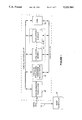
- FIG. 1 depicts a block diagram of a logic simulation system which includes a stimulus processor according to the present invention.
- FIGS. 2A and 2B when placed side-by-side, depict a block diagram of the stimulus processor architecture according to the present invention.
- FIGS. 3A, 3B, 3C and 3D when placed side-by-side, depict a block diagram of an event channel, which forms a portion of FIG. 2.
- FIG. 1 a block diagram of a logic simulator system 10 is depicted, which is connected to a suitable host computer 12 via a high speed data link 14.
- the logic simulator system 10 includes a configuration processor 20 which communicates by a configuration bus 22 to the other components depicted in the system 10.
- the logic simulator system 10 includes a stimulus processing hardware accelerator 30 which is connected to an event bus 24.
- the stimulus accelerator 30 provides high-speed presentation of stimulus events and run-time comparison of simulation outputs to expected outputs. Further details of the operation of the stimulus processing hardware accelerator 30 are described in more detail below.
- the configuration processor 30 communicates to a plurality of evaluator boards (such as evaluator boards 40-l through 40-N) which form the logic simulator.
- the logic simulator system 10 includes up to 15 evaluator boards, although other variations are possible.
- the logic simulator system 10 also includes a local random access memory (RAM) 28.
- RAM random access memory
- the configuration processor is connected to the accelerator 30, evaluator boards 40 and RAM 28 via the configuration bus 22.
- the accelerator 30, evaluator boards 40 and RAM 128 also communicate via the event bus 24.
- FIG. 2 a block diagram of the stimulus processing hardware accelerator 30 of FIG. 1 is depicted in more detail.
- a stimulus program is accessed through the RAM 28 of FIG. 1 through the memory interface 60 of FIG. 2 (specifically main memory part 62) under control of the processor system 70.
- Processor system 70 includes a control store 72, a sequencer 74, an external request decoder 76, a vector decoder 78 and an arithmetic and logic unit (ALU) 80.
- ALU arithmetic and logic unit
- Vector decoder 78 recognizes if an instruction in the stimulus program requires microcode operation (such as a loop) or if it is a simple event. The simple events are passed to the proper channel of event channels 100, as will be described. The more complex instructions are implemented in microcode and special purpose hardware.
- the stimulus processor architecture includes four event channels, which are channels 102, 104, 106 and 108. Each of the four channels in FIG. 2A are driven by an independent stimulus program.
- the event channels 100 are FIFO (first in, first out) based.
- the REQ signal on bus 86 is asserted. Then the REQ signal is deasserted and the processor system 70 switches to another event channel program in a round robin fashion.
- the events arrive at the channel output of event channels 100 out of time sequence.
- Hardware in the clock control logic 150 in FIG. 2B arbitrates between channels and evaluation units in the logic simulator (the evaluator boards 40 of FIG. 1) to insure that the events to the simulation are correctly time sorted.
- the output map section 130 comprises an output map index 132, a twelve bit counter 134 and an output map memory 136.
- the output map section 130 allows 512 pins from each channel to be mapped into any one of the nets supported by the logic simulator 40 of FIG. 1.
- the mapping algorithm reduces the number of bits required to store an event in memory, since the number of nets allowed in a simulation may be extremely large. However, the number of input and output signals from the simulation is held to a minimum by design.
- FIGS. 3A, 3B, 3C and 3D depict a block diagram of the event channel architecture depicted in FIGS. 2A and 2B.
- each event channel includes two subchannels, which are a vector channel 200 and a repetitive clock channel 210.
- the vector channel 200 accepts the vector input from the processor system 70 of FIG. 2A.
- the repetitive clock channel 210 generates repetitive signals without requiring continuous input from the processor system 70 of FIG. 2A.
- the channel select logic 250 multiplexes the vector channel 200 and repetitive clock channel 210 as a function of time to maturity for the waiting events on each channel.
- the comparator 254 compares the time to maturity for each channel and generates the RLT1 signal to both the channel select logic 250 and the channel select multiplexers 270,272.
- the DV bus 262 and VT bus 260 communicate with the stimulus engine clock control logic 150 of FIG. 2B.
- the VT bus 260 indicates to the clock control logic 150 how much time must elaspse before the next event matures in the channel.
- the DV bus 262 is used to control the incrementing logic in the clock control logic 150.
- the DT bus 152 of FIG. 2B is output with the amount of time which is elapsing (DT is delta time and is the amount of time that is advancing on the current clock tick).
- the DT bus 152 value is subtracted from the remaining time to maturity for the events in all of the event channels, and the simulation evaluation units.
- the time remaining to maturity is thereby reduced by the delta time (DT) and the new time to maturity is input by both subchannels (vector channel 200 and repetitive clock channel 210) to the channel select logic 250 of FIG. 3B.
- the Zero Detect Logic drives the Primary Out Register State Machine, generally indicated by numeral 264 of FIG. 3D, to allow the event to be presented to the simulator 40 of FIG. 1.
- the new value and strength for the pin is sourced by the PPIN register 266 of FIG. 3B.
- the subchannel which provides the new value and strength is multiplexed in the same manner as the time (i.e., the RLTI signal controls both channel select multiplexers 270, 272, as depicted in FIGS. 3B and 3D).
- the value and strength at the clock channel events is held in register 212.
- the value always toggles between logic 0, strength 2 and logic 1, strength 2, as controlled by the TQVAL signal.
- the value and strength for the event on the vector channel is determined by the input control state machine 100, which controls the PIN REG 202, the VALS REG 204 and the IVS logic 206.
- PIN REG 202 is a counter which can sequence PIN #'s for a bus which the individual PIN values are set into the VAL REG 204. The PIN #'s value is merged on to the IREG bus under control of the IVS logic 206.
Abstract
Description
Claims (6)
Applications Claiming Priority (2)
| Application Number | Priority Date | Filing Date | Title |
|---|---|---|---|
| US87845886A | 1986-06-25 | 1986-06-25 | |
| US34993289A | 1989-05-04 | 1989-05-04 |
Related Parent Applications (1)
| Application Number | Title | Priority Date | Filing Date |
|---|---|---|---|
| US34993289A Continuation | 1986-06-25 | 1989-05-04 |
Publications (1)
| Publication Number | Publication Date |
|---|---|
| US5126966A true US5126966A (en) | 1992-06-30 |
Family
ID=26996417
Family Applications (1)
| Application Number | Title | Priority Date | Filing Date |
|---|---|---|---|
| US07/467,297 Expired - Lifetime US5126966A (en) | 1986-06-25 | 1990-01-18 | High speed logic simulation system with stimulus engine using independent event channels selectively driven by independent stimulus programs |
Country Status (1)
| Country | Link |
|---|---|
| US (1) | US5126966A (en) |
Cited By (40)
| Publication number | Priority date | Publication date | Assignee | Title |
|---|---|---|---|---|
| US5353433A (en) * | 1990-09-06 | 1994-10-04 | Digital Equipment Corporation | Method and apparatus for organizing and analyzing timing information |
| US5465383A (en) * | 1989-11-15 | 1995-11-07 | Nec Corporation | System for forming test patterns for large scale integrated circuits |
| US5493672A (en) * | 1994-05-16 | 1996-02-20 | Sun Microsystems, Inc. | Concurrent simulation of host system at instruction level and input/output system at logic level with two-way communication deadlock resolution |
| US5530841A (en) * | 1990-12-21 | 1996-06-25 | Synopsys, Inc. | Method for converting a hardware independent user description of a logic circuit into hardware components |
| US5612891A (en) * | 1988-10-05 | 1997-03-18 | Quickturn Design Systems, Inc. | Hardware logic emulation system with memory capability |
| US5621651A (en) * | 1994-03-09 | 1997-04-15 | Texas Instruments Incorporated | Emulation devices, systems and methods with distributed control of test interfaces in clock domains |
| US5625580A (en) | 1989-05-31 | 1997-04-29 | Synopsys, Inc. | Hardware modeling system and method of use |
| US5649164A (en) * | 1994-12-30 | 1997-07-15 | International Business Machines Corporation | Sets and holds in virtual time logic simulation for parallel processors |
| US5680583A (en) * | 1994-02-16 | 1997-10-21 | Arkos Design, Inc. | Method and apparatus for a trace buffer in an emulation system |
| US5819065A (en) * | 1995-06-28 | 1998-10-06 | Quickturn Design Systems, Inc. | System and method for emulating memory |
| US5822564A (en) * | 1996-06-03 | 1998-10-13 | Quickturn Design Systems, Inc. | Checkpointing in an emulation system |
| US5841967A (en) | 1996-10-17 | 1998-11-24 | Quickturn Design Systems, Inc. | Method and apparatus for design verification using emulation and simulation |
| US5920712A (en) * | 1994-05-13 | 1999-07-06 | Quickturn Design Systems, Inc. | Emulation system having multiple emulator clock cycles per emulated clock cycle |
| US5920490A (en) * | 1996-12-26 | 1999-07-06 | Adaptec, Inc. | Integrated circuit test stimulus verification and vector extraction system |
| US5923865A (en) * | 1995-06-28 | 1999-07-13 | Quickturn Design Systems, Inc. | Emulation system having multiple emulated clock cycles per emulator clock cycle and improved signal routing |
| US5960191A (en) | 1997-05-30 | 1999-09-28 | Quickturn Design Systems, Inc. | Emulation system with time-multiplexed interconnect |
| US5970240A (en) | 1997-06-25 | 1999-10-19 | Quickturn Design Systems, Inc. | Method and apparatus for configurable memory emulation |
| US6009256A (en) * | 1997-05-02 | 1999-12-28 | Axis Systems, Inc. | Simulation/emulation system and method |
| US6026230A (en) * | 1997-05-02 | 2000-02-15 | Axis Systems, Inc. | Memory simulation system and method |
| US6058252A (en) * | 1995-01-19 | 2000-05-02 | Synopsys, Inc. | System and method for generating effective layout constraints for a circuit design or the like |
| US6074428A (en) * | 1994-10-19 | 2000-06-13 | Hewlett-Packard Company | Minimizing logic by resolving "don't care" output values in a finite state machine |
| US6134516A (en) * | 1997-05-02 | 2000-10-17 | Axis Systems, Inc. | Simulation server system and method |
| US6148275A (en) | 1989-05-31 | 2000-11-14 | Synopsys, Inc. | System for and method of connecting a hardware modeling element to a hardware modeling system |
| US6321366B1 (en) | 1997-05-02 | 2001-11-20 | Axis Systems, Inc. | Timing-insensitive glitch-free logic system and method |
| US6389379B1 (en) | 1997-05-02 | 2002-05-14 | Axis Systems, Inc. | Converification system and method |
| US6421823B1 (en) * | 1991-04-11 | 2002-07-16 | Agilent Technologies, Inc. | Bidirectional socket stimulus interface for a logic simulator |
| US6421251B1 (en) | 1997-05-02 | 2002-07-16 | Axis Systems Inc | Array board interconnect system and method |
| US6449659B1 (en) | 1997-07-14 | 2002-09-10 | Microsoft Corporation | System for instance customization with application independent programming of controls |
| US20030188278A1 (en) * | 2002-03-26 | 2003-10-02 | Carrie Susan Elizabeth | Method and apparatus for accelerating digital logic simulations |
| US6718534B1 (en) | 1997-07-14 | 2004-04-06 | Microsoft Corporation | System for application independent programming of controls |
| US20050154559A1 (en) * | 2004-01-12 | 2005-07-14 | International Business Machines Corporation | System and method for heuristically optimizing a large set of automated test sets |
| US20050267727A1 (en) * | 2004-06-01 | 2005-12-01 | Quickturn Design Systems, Inc. | System and method for providing flexible signal routing and timing |
| US20050267728A1 (en) * | 2004-06-01 | 2005-12-01 | Quickturn Design Systems, Inc. | System and method for reliably supporting multiple signaling technologies |
| US20050267729A1 (en) * | 2004-06-01 | 2005-12-01 | Quickturn Design Systems, Inc. | Extensible memory architecture and communication protocol for supporting multiple devices in low-bandwidth, asynchronous applications |
| US20050271078A1 (en) * | 2004-06-01 | 2005-12-08 | Quayle Barton L | System and method for configuring communication systems |
| US20050278163A1 (en) * | 2004-06-01 | 2005-12-15 | Quickturn Design Systems, Inc. | System and method for resolving artifacts in differential signals |
| US20060253762A1 (en) * | 2005-03-16 | 2006-11-09 | Schalick Christopher A | FPGA emulation system |
| US7555424B2 (en) | 2006-03-16 | 2009-06-30 | Quickturn Design Systems, Inc. | Method and apparatus for rewinding emulated memory circuits |
| EP2721508A1 (en) * | 2011-06-14 | 2014-04-23 | Montana Systems Inc. | System, method and apparatus for a scalable parallel processor |
| RU219215U1 (en) * | 2023-02-22 | 2023-07-05 | Федеральное государственное бюджетное учреждение "4 Центральный научно-исследовательский институт" Министерства обороны Российской Федерации | Device for simulating independent events |
Citations (26)
| Publication number | Priority date | Publication date | Assignee | Title |
|---|---|---|---|---|
| US3961250A (en) * | 1974-05-08 | 1976-06-01 | International Business Machines Corporation | Logic network test system with simulator oriented fault test generator |
| US4066882A (en) * | 1976-08-16 | 1978-01-03 | Grumman Aerospace Corporation | Digital stimulus generating and response measuring means |
| US4161276A (en) * | 1978-03-01 | 1979-07-17 | Ncr Corporation | Complex logical fault detection apparatus and method |
| US4306286A (en) * | 1979-06-29 | 1981-12-15 | International Business Machines Corporation | Logic simulation machine |
| US4316259A (en) * | 1980-03-18 | 1982-02-16 | Grumman Aerospace Corporation | Programmable function generator |
| US4342093A (en) * | 1979-05-15 | 1982-07-27 | Hitachi, Ltd. | Method of digital logic simulation |
| US4527249A (en) * | 1982-10-22 | 1985-07-02 | Control Data Corporation | Simulator system for logic design validation |
| US4571724A (en) * | 1983-03-23 | 1986-02-18 | Data I/O Corporation | System for testing digital logic devices |
| US4587625A (en) * | 1983-07-05 | 1986-05-06 | Motorola Inc. | Processor for simulating digital structures |
| US4594677A (en) * | 1983-11-09 | 1986-06-10 | International Business Machines Corporation | System for detecting and diagnosing noise caused by simultaneous current switching |
| US4601032A (en) * | 1983-10-17 | 1986-07-15 | Cirrus Computers Ltd. | Test-generation system for digital circuits |
| US4622647A (en) * | 1982-07-27 | 1986-11-11 | Rank Xerox Sa | System for the automatic testing of printed circuits |
| US4628471A (en) * | 1984-02-02 | 1986-12-09 | Prime Computer, Inc. | Digital system simulation method and apparatus having two signal-level modes of operation |
| US4644487A (en) * | 1983-04-09 | 1987-02-17 | International Computers Limited | Method and apparatus for verifying the design of digital electronic components |
| US4656580A (en) * | 1982-06-11 | 1987-04-07 | International Business Machines Corporation | Logic simulation machine |
| US4656632A (en) * | 1983-11-25 | 1987-04-07 | Giordano Associates, Inc. | System for automatic testing of circuits and systems |
| US4725975A (en) * | 1982-07-13 | 1988-02-16 | Nec Corporation | Logic simulator operable on level basis and on logic block basis on each level |
| US4744084A (en) * | 1986-02-27 | 1988-05-10 | Mentor Graphics Corporation | Hardware modeling system and method for simulating portions of electrical circuits |
| US4747102A (en) * | 1985-03-30 | 1988-05-24 | Nec Corporation | Method of controlling a logical simulation at a high speed |
| US4751637A (en) * | 1984-03-28 | 1988-06-14 | Daisy Systems Corporation | Digital computer for implementing event driven simulation algorithm |
| US4763288A (en) * | 1985-12-31 | 1988-08-09 | Schlumberger Systems & Services, Inc. | System for simulating electronic digital circuits |
| US4769817A (en) * | 1986-01-31 | 1988-09-06 | Zycad Corporation | Concurrent fault simulation for logic designs |
| US4775950A (en) * | 1984-11-02 | 1988-10-04 | Mitsubishi Denki Kabushiki Kaisha | Logic simulation system |
| US4782440A (en) * | 1984-08-03 | 1988-11-01 | Nec Corporation | Logic simulator using small capacity memories for storing logic states, connection patterns, and logic functions |
| US4791578A (en) * | 1986-12-30 | 1988-12-13 | Eta Systems, Inc. | Logic gate system design |
| US4821173A (en) * | 1986-06-30 | 1989-04-11 | Motorola, Inc. | Wired "OR" bus evaluator for logic simulation |
-
1990
- 1990-01-18 US US07/467,297 patent/US5126966A/en not_active Expired - Lifetime
Patent Citations (26)
| Publication number | Priority date | Publication date | Assignee | Title |
|---|---|---|---|---|
| US3961250A (en) * | 1974-05-08 | 1976-06-01 | International Business Machines Corporation | Logic network test system with simulator oriented fault test generator |
| US4066882A (en) * | 1976-08-16 | 1978-01-03 | Grumman Aerospace Corporation | Digital stimulus generating and response measuring means |
| US4161276A (en) * | 1978-03-01 | 1979-07-17 | Ncr Corporation | Complex logical fault detection apparatus and method |
| US4342093A (en) * | 1979-05-15 | 1982-07-27 | Hitachi, Ltd. | Method of digital logic simulation |
| US4306286A (en) * | 1979-06-29 | 1981-12-15 | International Business Machines Corporation | Logic simulation machine |
| US4316259A (en) * | 1980-03-18 | 1982-02-16 | Grumman Aerospace Corporation | Programmable function generator |
| US4656580A (en) * | 1982-06-11 | 1987-04-07 | International Business Machines Corporation | Logic simulation machine |
| US4725975A (en) * | 1982-07-13 | 1988-02-16 | Nec Corporation | Logic simulator operable on level basis and on logic block basis on each level |
| US4622647A (en) * | 1982-07-27 | 1986-11-11 | Rank Xerox Sa | System for the automatic testing of printed circuits |
| US4527249A (en) * | 1982-10-22 | 1985-07-02 | Control Data Corporation | Simulator system for logic design validation |
| US4571724A (en) * | 1983-03-23 | 1986-02-18 | Data I/O Corporation | System for testing digital logic devices |
| US4644487A (en) * | 1983-04-09 | 1987-02-17 | International Computers Limited | Method and apparatus for verifying the design of digital electronic components |
| US4587625A (en) * | 1983-07-05 | 1986-05-06 | Motorola Inc. | Processor for simulating digital structures |
| US4601032A (en) * | 1983-10-17 | 1986-07-15 | Cirrus Computers Ltd. | Test-generation system for digital circuits |
| US4594677A (en) * | 1983-11-09 | 1986-06-10 | International Business Machines Corporation | System for detecting and diagnosing noise caused by simultaneous current switching |
| US4656632A (en) * | 1983-11-25 | 1987-04-07 | Giordano Associates, Inc. | System for automatic testing of circuits and systems |
| US4628471A (en) * | 1984-02-02 | 1986-12-09 | Prime Computer, Inc. | Digital system simulation method and apparatus having two signal-level modes of operation |
| US4751637A (en) * | 1984-03-28 | 1988-06-14 | Daisy Systems Corporation | Digital computer for implementing event driven simulation algorithm |
| US4782440A (en) * | 1984-08-03 | 1988-11-01 | Nec Corporation | Logic simulator using small capacity memories for storing logic states, connection patterns, and logic functions |
| US4775950A (en) * | 1984-11-02 | 1988-10-04 | Mitsubishi Denki Kabushiki Kaisha | Logic simulation system |
| US4747102A (en) * | 1985-03-30 | 1988-05-24 | Nec Corporation | Method of controlling a logical simulation at a high speed |
| US4763288A (en) * | 1985-12-31 | 1988-08-09 | Schlumberger Systems & Services, Inc. | System for simulating electronic digital circuits |
| US4769817A (en) * | 1986-01-31 | 1988-09-06 | Zycad Corporation | Concurrent fault simulation for logic designs |
| US4744084A (en) * | 1986-02-27 | 1988-05-10 | Mentor Graphics Corporation | Hardware modeling system and method for simulating portions of electrical circuits |
| US4821173A (en) * | 1986-06-30 | 1989-04-11 | Motorola, Inc. | Wired "OR" bus evaluator for logic simulation |
| US4791578A (en) * | 1986-12-30 | 1988-12-13 | Eta Systems, Inc. | Logic gate system design |
Cited By (61)
| Publication number | Priority date | Publication date | Assignee | Title |
|---|---|---|---|---|
| US5661662A (en) * | 1988-10-05 | 1997-08-26 | Quickturn Design Systems, Inc. | Structures and methods for adding stimulus and response functions to a circuit design undergoing emulation |
| US5812414A (en) * | 1988-10-05 | 1998-09-22 | Quickturn Design Systems, Inc. | Method for performing simulation using a hardware logic emulation system |
| US5612891A (en) * | 1988-10-05 | 1997-03-18 | Quickturn Design Systems, Inc. | Hardware logic emulation system with memory capability |
| US5796623A (en) * | 1988-10-05 | 1998-08-18 | Quickturn Design Systems, Inc. | Apparatus and method for performing computations with electrically reconfigurable logic devices |
| US5657241A (en) * | 1988-10-05 | 1997-08-12 | Quickturn Design Systems, Inc. | Routing methods for use in a logic emulation system |
| US6148275A (en) | 1989-05-31 | 2000-11-14 | Synopsys, Inc. | System for and method of connecting a hardware modeling element to a hardware modeling system |
| US5625580A (en) | 1989-05-31 | 1997-04-29 | Synopsys, Inc. | Hardware modeling system and method of use |
| US5465383A (en) * | 1989-11-15 | 1995-11-07 | Nec Corporation | System for forming test patterns for large scale integrated circuits |
| US5353433A (en) * | 1990-09-06 | 1994-10-04 | Digital Equipment Corporation | Method and apparatus for organizing and analyzing timing information |
| US5748488A (en) * | 1990-12-21 | 1998-05-05 | Synopsys, Inc. | Method for generating a logic circuit from a hardware independent user description using assignment conditions |
| US5680318A (en) * | 1990-12-21 | 1997-10-21 | Synopsys Inc. | Synthesizer for generating a logic network using a hardware independent description |
| US5691911A (en) * | 1990-12-21 | 1997-11-25 | Synopsys, Inc. | Method for pre-processing a hardware independent description of a logic circuit |
| US5737574A (en) * | 1990-12-21 | 1998-04-07 | Synopsys, Inc | Method for generating a logic circuit from a hardware independent user description using mux conditions and hardware selectors |
| US5661661A (en) * | 1990-12-21 | 1997-08-26 | Synopsys, Inc. | Method for processing a hardware independent user description to generate logic circuit elements including flip-flops, latches, and three-state buffers and combinations thereof |
| US5530841A (en) * | 1990-12-21 | 1996-06-25 | Synopsys, Inc. | Method for converting a hardware independent user description of a logic circuit into hardware components |
| US6421823B1 (en) * | 1991-04-11 | 2002-07-16 | Agilent Technologies, Inc. | Bidirectional socket stimulus interface for a logic simulator |
| US5680583A (en) * | 1994-02-16 | 1997-10-21 | Arkos Design, Inc. | Method and apparatus for a trace buffer in an emulation system |
| US5884066A (en) | 1994-02-16 | 1999-03-16 | Quickturn Design Systems, Inc. | Method and apparatus for a trace buffer in an emulation system |
| US5621651A (en) * | 1994-03-09 | 1997-04-15 | Texas Instruments Incorporated | Emulation devices, systems and methods with distributed control of test interfaces in clock domains |
| US5920712A (en) * | 1994-05-13 | 1999-07-06 | Quickturn Design Systems, Inc. | Emulation system having multiple emulator clock cycles per emulated clock cycle |
| US5493672A (en) * | 1994-05-16 | 1996-02-20 | Sun Microsystems, Inc. | Concurrent simulation of host system at instruction level and input/output system at logic level with two-way communication deadlock resolution |
| US6074428A (en) * | 1994-10-19 | 2000-06-13 | Hewlett-Packard Company | Minimizing logic by resolving "don't care" output values in a finite state machine |
| US5649164A (en) * | 1994-12-30 | 1997-07-15 | International Business Machines Corporation | Sets and holds in virtual time logic simulation for parallel processors |
| US6058252A (en) * | 1995-01-19 | 2000-05-02 | Synopsys, Inc. | System and method for generating effective layout constraints for a circuit design or the like |
| US5819065A (en) * | 1995-06-28 | 1998-10-06 | Quickturn Design Systems, Inc. | System and method for emulating memory |
| US5923865A (en) * | 1995-06-28 | 1999-07-13 | Quickturn Design Systems, Inc. | Emulation system having multiple emulated clock cycles per emulator clock cycle and improved signal routing |
| US5822564A (en) * | 1996-06-03 | 1998-10-13 | Quickturn Design Systems, Inc. | Checkpointing in an emulation system |
| US6058492A (en) | 1996-10-17 | 2000-05-02 | Quickturn Design Systems, Inc. | Method and apparatus for design verification using emulation and simulation |
| US5841967A (en) | 1996-10-17 | 1998-11-24 | Quickturn Design Systems, Inc. | Method and apparatus for design verification using emulation and simulation |
| US5920490A (en) * | 1996-12-26 | 1999-07-06 | Adaptec, Inc. | Integrated circuit test stimulus verification and vector extraction system |
| US6134516A (en) * | 1997-05-02 | 2000-10-17 | Axis Systems, Inc. | Simulation server system and method |
| US6026230A (en) * | 1997-05-02 | 2000-02-15 | Axis Systems, Inc. | Memory simulation system and method |
| US6009256A (en) * | 1997-05-02 | 1999-12-28 | Axis Systems, Inc. | Simulation/emulation system and method |
| US6321366B1 (en) | 1997-05-02 | 2001-11-20 | Axis Systems, Inc. | Timing-insensitive glitch-free logic system and method |
| US6389379B1 (en) | 1997-05-02 | 2002-05-14 | Axis Systems, Inc. | Converification system and method |
| US6421251B1 (en) | 1997-05-02 | 2002-07-16 | Axis Systems Inc | Array board interconnect system and method |
| US6377912B1 (en) | 1997-05-30 | 2002-04-23 | Quickturn Design Systems, Inc. | Emulation system with time-multiplexed interconnect |
| US5960191A (en) | 1997-05-30 | 1999-09-28 | Quickturn Design Systems, Inc. | Emulation system with time-multiplexed interconnect |
| US5970240A (en) | 1997-06-25 | 1999-10-19 | Quickturn Design Systems, Inc. | Method and apparatus for configurable memory emulation |
| US6449659B1 (en) | 1997-07-14 | 2002-09-10 | Microsoft Corporation | System for instance customization with application independent programming of controls |
| US6718534B1 (en) | 1997-07-14 | 2004-04-06 | Microsoft Corporation | System for application independent programming of controls |
| US20030188278A1 (en) * | 2002-03-26 | 2003-10-02 | Carrie Susan Elizabeth | Method and apparatus for accelerating digital logic simulations |
| US20050154559A1 (en) * | 2004-01-12 | 2005-07-14 | International Business Machines Corporation | System and method for heuristically optimizing a large set of automated test sets |
| US6975965B2 (en) | 2004-01-12 | 2005-12-13 | International Business Machines Corporation | System and method for heuristically optimizing a large set of automated test sets |
| US7738398B2 (en) | 2004-06-01 | 2010-06-15 | Quickturn Design Systems, Inc. | System and method for configuring communication systems |
| US20050267727A1 (en) * | 2004-06-01 | 2005-12-01 | Quickturn Design Systems, Inc. | System and method for providing flexible signal routing and timing |
| US7606697B2 (en) | 2004-06-01 | 2009-10-20 | Quickturn Design Systems, Inc. | System and method for resolving artifacts in differential signals |
| US20050267728A1 (en) * | 2004-06-01 | 2005-12-01 | Quickturn Design Systems, Inc. | System and method for reliably supporting multiple signaling technologies |
| US7640155B2 (en) | 2004-06-01 | 2009-12-29 | Quickturn Design Systems, Inc. | Extensible memory architecture and communication protocol for supporting multiple devices in low-bandwidth, asynchronous applications |
| US20050267729A1 (en) * | 2004-06-01 | 2005-12-01 | Quickturn Design Systems, Inc. | Extensible memory architecture and communication protocol for supporting multiple devices in low-bandwidth, asynchronous applications |
| US7440866B2 (en) | 2004-06-01 | 2008-10-21 | Quickturn Design Systems Inc. | System and method for validating an input/output voltage of a target system |
| US7721036B2 (en) | 2004-06-01 | 2010-05-18 | Quickturn Design Systems Inc. | System and method for providing flexible signal routing and timing |
| US20050271078A1 (en) * | 2004-06-01 | 2005-12-08 | Quayle Barton L | System and method for configuring communication systems |
| US20050278163A1 (en) * | 2004-06-01 | 2005-12-15 | Quickturn Design Systems, Inc. | System and method for resolving artifacts in differential signals |
| US20060253762A1 (en) * | 2005-03-16 | 2006-11-09 | Schalick Christopher A | FPGA emulation system |
| US8000954B2 (en) | 2005-03-16 | 2011-08-16 | Gaterocket, Inc. | FPGA emulation system |
| US7555424B2 (en) | 2006-03-16 | 2009-06-30 | Quickturn Design Systems, Inc. | Method and apparatus for rewinding emulated memory circuits |
| EP2721508A1 (en) * | 2011-06-14 | 2014-04-23 | Montana Systems Inc. | System, method and apparatus for a scalable parallel processor |
| EP2721508A4 (en) * | 2011-06-14 | 2015-04-01 | Montana Systems Inc | System, method and apparatus for a scalable parallel processor |
| US9430596B2 (en) | 2011-06-14 | 2016-08-30 | Montana Systems Inc. | System, method and apparatus for a scalable parallel processor |
| RU219215U1 (en) * | 2023-02-22 | 2023-07-05 | Федеральное государственное бюджетное учреждение "4 Центральный научно-исследовательский институт" Министерства обороны Российской Федерации | Device for simulating independent events |
Similar Documents
| Publication | Publication Date | Title |
|---|---|---|
| US5126966A (en) | High speed logic simulation system with stimulus engine using independent event channels selectively driven by independent stimulus programs | |
| EP0021404B1 (en) | Computing system for the simulation of logic operations | |
| US4787061A (en) | Dual delay mode pipelined logic simulator | |
| US4782461A (en) | Logical grouping of facilities within a computer development system | |
| US5572666A (en) | System and method for generating pseudo-random instructions for design verification | |
| US5841967A (en) | Method and apparatus for design verification using emulation and simulation | |
| US5715433A (en) | Dynamic software model for emulating hardware | |
| KR100759600B1 (en) | Digital circuit implementation by means of parallel sequencers | |
| US7930162B1 (en) | Accelerating hardware co-simulation using dynamic replay on first-in-first-out-driven command processor | |
| EP0096176A2 (en) | Method of logic simulation and logic simulation machine | |
| US6523155B1 (en) | Method for partitioning a netlist into multiple clock domains | |
| JPH0727538B2 (en) | Logic simulation method and apparatus using hardware accelerator | |
| US3953833A (en) | Microprogrammable computer having a dual function secondary storage element | |
| US4443848A (en) | Two-level priority circuit | |
| EP0025087A2 (en) | Pipeline Control apparatus for generating Instructions in a Digital Computer | |
| US5923865A (en) | Emulation system having multiple emulated clock cycles per emulator clock cycle and improved signal routing | |
| JPH08320808A (en) | Emulation system | |
| US5097468A (en) | Testing asynchronous processes | |
| Welch | Emulating digital logic using transputer networks (very high parallelism= simplicity= performance) | |
| EP1845462A1 (en) | Hardware emulations system for integrated circuits having a heterogeneous cluster of processors | |
| KR910001054B1 (en) | Apparatus and method for a microprogrammed data processing system having a plurality of control stores | |
| US5774368A (en) | Controller structure template and method for designing a controller structure | |
| JP3212709B2 (en) | Logic simulation device | |
| US7464017B2 (en) | Time multiplexed interface for emulator system | |
| Welch | Emulating digital logic using transputer networks (very high parallelism= simplicity= performance) |
Legal Events
| Date | Code | Title | Description |
|---|---|---|---|
| FPAY | Fee payment |
Year of fee payment: 4 |
|
| REMI | Maintenance fee reminder mailed | ||
| FP | Lapsed due to failure to pay maintenance fee |
Effective date: 20000630 |
|
| FEPP | Fee payment procedure |
Free format text: PETITION RELATED TO MAINTENANCE FEES FILED (ORIGINAL EVENT CODE: PMFP); ENTITY STATUS OF PATENT OWNER: LARGE ENTITY |
|
| FEPP | Fee payment procedure |
Free format text: PETITION RELATED TO MAINTENANCE FEES GRANTED (ORIGINAL EVENT CODE: PMFG); ENTITY STATUS OF PATENT OWNER: LARGE ENTITY |
|
| FPAY | Fee payment |
Year of fee payment: 8 |
|
| SULP | Surcharge for late payment | ||
| STCF | Information on status: patent grant |
Free format text: PATENTED CASE |
|
| PRDP | Patent reinstated due to the acceptance of a late maintenance fee |
Effective date: 20010713 |
|
| FEPP | Fee payment procedure |
Free format text: PAT HOLDER NO LONGER CLAIMS SMALL ENTITY STATUS, ENTITY STATUS SET TO UNDISCOUNTED (ORIGINAL EVENT CODE: STOL); ENTITY STATUS OF PATENT OWNER: LARGE ENTITY |
|
| FPAY | Fee payment |
Year of fee payment: 12 |
|
| REFU | Refund |
Free format text: REFUND - PAYMENT OF MAINTENANCE FEE, 12TH YR, SMALL ENTITY (ORIGINAL EVENT CODE: R2553); ENTITY STATUS OF PATENT OWNER: LARGE ENTITY |
|
| FEPP | Fee payment procedure |
Free format text: ENTITY STATUS SET TO UNDISCOUNTED (ORIGINAL EVENT CODE: BIG.); ENTITY STATUS OF PATENT OWNER: LARGE ENTITY |
|
| AS | Assignment |
Owner name: MENTOR GRAPHICS CORPORATION, OREGON Free format text: ASSIGNMENT OF ASSIGNORS INTEREST;ASSIGNOR:IKOS SYSTEMS, INC.;REEL/FRAME:016561/0467 Effective date: 20050826 |
|
| FEPP | Fee payment procedure |
Free format text: PAYOR NUMBER ASSIGNED (ORIGINAL EVENT CODE: ASPN); ENTITY STATUS OF PATENT OWNER: LARGE ENTITY |