US5187680A - Neural net using capacitive structures connecting input lines and differentially sensed output line pairs - Google Patents
Neural net using capacitive structures connecting input lines and differentially sensed output line pairs Download PDFInfo
- Publication number
- US5187680A US5187680A US07/810,431 US81043191A US5187680A US 5187680 A US5187680 A US 5187680A US 81043191 A US81043191 A US 81043191A US 5187680 A US5187680 A US 5187680A
- Authority
- US
- United States
- Prior art keywords
- input
- output
- identified
- lines
- processor
- Prior art date
- Legal status (The legal status is an assumption and is not a legal conclusion. Google has not performed a legal analysis and makes no representation as to the accuracy of the status listed.)
- Expired - Lifetime
Links
Images


Classifications
-
- G—PHYSICS
- G06—COMPUTING; CALCULATING OR COUNTING
- G06N—COMPUTING ARRANGEMENTS BASED ON SPECIFIC COMPUTATIONAL MODELS
- G06N3/00—Computing arrangements based on biological models
- G06N3/02—Neural networks
- G06N3/06—Physical realisation, i.e. hardware implementation of neural networks, neurons or parts of neurons
- G06N3/063—Physical realisation, i.e. hardware implementation of neural networks, neurons or parts of neurons using electronic means
- G06N3/065—Analogue means
Landscapes
- Engineering & Computer Science (AREA)
- Physics & Mathematics (AREA)
- Health & Medical Sciences (AREA)
- Life Sciences & Earth Sciences (AREA)
- Biomedical Technology (AREA)
- Biophysics (AREA)
- Theoretical Computer Science (AREA)
- Evolutionary Computation (AREA)
- Computational Linguistics (AREA)
- Data Mining & Analysis (AREA)
- Artificial Intelligence (AREA)
- General Health & Medical Sciences (AREA)
- Molecular Biology (AREA)
- Computing Systems (AREA)
- General Engineering & Computer Science (AREA)
- General Physics & Mathematics (AREA)
- Mathematical Physics (AREA)
- Software Systems (AREA)
- Neurology (AREA)
- Logic Circuits (AREA)
Abstract
Neural nets using capacitive structures are adapted for construction in complementary metal-oxide-semiconductor integrated-circuit technology. In each neural net layer synapse input signals are applied to the inverting and non-inverting input terminals of each of a plurality of differential-input non-linear amplifiers by a respective pair of capacitors, which non-linear amplifiers generate respective axon responses. In certain of these neural nets, arrangements are described that make the capacitive structures bilaterally responsive, so that back-propagation calculations can be performed to alter the relative values of capacitors in each pair thereof, which is done during training of certain of the neural nets described.
Description
This application is a continuation of application Ser. No. 07/366,838, filed Jun. 15, 1989, now abandoned.
The invention relates to computer structures that emulate portions of a brain in operation, and more particularly, to such computer structures as can be realized using complementary metal-oxide-semiconductor (CMOS) technology.
A patent application Ser. No. 366,839, now U.S. Pat. No. 5,146,542, concurrently filed by the inventor, entitled NEURAL NET USING CAPACITIVE STRUCTURES CONNECTING OUTPUT LINES AND DIFFERENTIALLY DRIVEN INPUT LINE PAIRS and assigned to General Electric Company, discloses alternative neural net structures to those described herein.
Computers of the von Neumann type architecture have limited computational speed owing to the communication limitations of the single processor. These limitations may be overcome if a plurality of processors are utilized in the calculation and are operated at least partly in parallel. This alternative architecture, however, generally leads to difficulties associated with programming complexity. Therefore, it is often not a good solution. Recently, an entirely different alternative that does not require programming has shown promise. The networking ability of the neurons in the brain has served as a model for the formation of a highly interconnected set of processors, called a "neural network" or "neural net" that can provide computational and reasoning functions without the need of formal programming. The neural nets can learn the correct procedure by experience rather than being preprogrammed for performing the correct procedure. The reader is referred to R.P. Lippmann's article "An Introduction to Computing With Neural Nets" appearing on pages 4-21 of the April 1987 IEEE ASSP MAGAZINE (07407467/87/0400-0004/$10.00" 1987 IEEE), incorporated herein by reference, for background about the state of the art in regard to neural nets.
Neural nets are composed of a plurality of neuron models, processors each exhibiting "axon" output signal response to a plurality of "synapse" input signals. In a type of neural net called a "perceptron", each of these processors calculates the weighted sum of its "synapse" input signals, which are respectively weighted by respective weighting values that may be positive- or negative-valued, and responds non-linearly to the weighted sum to generate the "axon" output response. This relationship may be described in mathematical symbols as follows. ##EQU1##
Here, i indexes the input signals of the perceptron, of which there are an integral number M, and j indexes its output signals, of which there are an integral number N. Wi,j is the weighting of the ith input signal as makes up the jth output signal at such low input signal levels that the function ##EQU2## is approximately linear. At higher absolute values of its argument, the function ##EQU3## no longer exhibits linearity but rather exhibits a reduced response to ##EQU4##
A more complex artificial neural network arranges a plurality of perceptrons in hierarchic layers, the output signals of each earlier layer providing input signals for the next succeeding layer. Those layers preceding the output layer providing the ultimate output signal(s) are called "hidden" layers.
The processing just described normally involves sampled-data analog signals, and prior-art neural nets have employed operational amplifiers with resistive interconnecting elements for the weighting and summing procedures. The resistive elements implement weighted summation being done in accordance with Ohm's Law. The speed of such a processor is limited by capacitances in various portions of the processor, and computations have been slow if the power consumption of a reasonably large neural net is to be held within reasonable bounds. That is, speed is increased by reducing resistance values to reduce RC time constants in the processors, but the reduced resistance values increase the V2 /R power consumption (R, C and V being resistance, capacitance and voltage, respectively.)
Using capacitors to perform weighted summation in accordance with Coulomb's Law can provide neural nets of given size operating at given speed that consume less power than those the processors of which use conductive elements such as resistors to implement weighted summation in accordance with Ohm's Law.
This metal-oxide-metal construction of capacitors is described in detail by the inventor in his U.S. Pat. No. 3,691,627 issued Sep. 19, 1972, entitled "METHOD OF FABRICATING BURIED METALLIC FILM DEVICES", assigned to General Electric Company and incorporated by reference herein. In the inventor's U.S. Pat. No. 4,156,284 issued May 22, 1979, entitled "SIGNAL PROCESSING APPARATUS" and assigned to General Electric Company the use of a metal-oxide-metal construction of capacitors in the construction of arrays of weighting capacitors in an MOS integrated circuit is described in connection with apparatus for performing matrix multiplication.
Y.P. Tsividis and D. Anastassion in a letter "Switched-Capacitor Neural Networks" appearing in ELECTRONICS LETTERS, Aug. 27, 1987, Vol. 23, No. 18, pages 958, 959 (IEE) describe one method of implementing weighted summation in accordance with Coulomb's Law. Their method, a switched capacitor method, is useful in analog sampled-data neural net systems. However, a method of implementing weighted summation in accordance with Coulomb's Law that does not rely on capacitances being switched is highly desirable, it is here pointed out. This avoids the complexity of the capacitor switching elements and associated control lines. Furthermore, operation of the neural net with continuous analog signals over sustained periods of time, as well as with sampled data analog signals, is thus made possible.
A problem that is encountered when one attempts to use capacitors to perform weighted summation in a neural net layer is associated with the stray capacitance between input and output lines, which tends to be of appreciable size in neural net layers constructed using a metal-oxide-semiconductor (MOS) integrated circuit technology. The input and output lines are usually laid out as overlapping column and row busses using plural-layer metallization. The column busses are situated in one layer of metallization and the row busses are situated in another layer of metallization separated from the other layer by an intervening insulating oxide layer. This oxide layer is thin, so there is appreciable capacitance at each crossing of one bus over another. The fact of the row and column busses being in different planes tends to increase stray capacitances between them. The stray capacitance problem is also noted where both row and column busses are situated in the same metallization layer with one set of busses being periodically interrupted in their self-connections to allow passage of the other set of busses and being provided with cross-over connections to complete their self-connections. The problem of stray capacitance is compounded by the fact that the capacitive elements used to provide weights in a capacitive voltage summation network have stray capacitances to the substrate of the monolithic integrated circuit in which they are incorporated; a perfect two-terminal capacitance is not actually available in the monolithic integrated circuit. Where capacitive elements having programmable capacitances are used, capacitance is usually not programmable to zero value, either.
The problems of stray capacitance are solved in the invention by using output line pairs and sensing the charge conditions on the output lines of each pair differentially so that the effects of stray capacitances tend to cancel each other out. These output line pairs facilitate both excitory and inhibitory weights--that is, both positive- and negative-polarity Wi,j --in effect to be achieved without having to resort to capacitor switching to achieve negative capacitance.
Neural nets employing capacitors in accordance with the invention lend themselves to being used in performing parts of the computations needed to implement a back-propagation training algorithm. The back-propagation training algorithm is an iterative gradient algorithm designed to minimize the mean square error between the actual output of a multi-layer feed-forward neural net and the desired output. It requires continuous, differentiable non-linearities. A recursive algorithm starting at the output nodes and working back to the first hidden layer is used iteratively to adjust weights in accordance with the following formula.
W.sub.i,j (t+1)=W.sub.i,j (t)-ηδ.sub.j x.sub.i ( 2)
In this equation Wi,j (t) is the weight from hidden node i (or, in the case of the first hidden layer, from an input node) to node j at time t; xi is either the output of node i (or, in the case of the first hidden layer, is an input signal); η is a gain term introduced to maintain stability in the feedback procedure used to minimize the mean square errors between the actual output(s) of the perceptron and its desired output(s); and δj is a derivative of error. The general definition of δj is the change in error energy from output node j of a neural net layer with a change in the weighted summation of the input signals used to supply that output node j.
Lippman presumes that a particular sigmoid logistic non-linearity is used. Presuming the non-linearity of processor response is to be defined not as restrictively as Lippmann does, then δj can be more particularly defined as in equation (2), following, if node j is an output node, or as in equation (3), following, if node j is an internal hidden node. ##EQU5## In equation (3) dj and yj are the desired and actual values of output response from the output layer and yj ' is differential response of yj to the non-linearity in the output layer--i.e., the slope of the transfer function of that non-linearity. In equation (4) k is over all nodes in the neural net layer succeeding the hidden node j under consideration and Wj,k is the weight between node j and each such node k. The term yj ' is defined in the same way as in equation (3).
The general definition of the yj ' term appearing in equations (3) and (4), rather than that general term being replaced by the specific value of yj ' associated with a sigmoid logistic non-linearity, is the primary difference between the training algorithm as described here and as described by Lippmann. Also, Lippmann defines δj in opposite polarity from equations (1), (3) and (4) above.
During training of the neural net, prescribed patterns of input signals are sequentially repetitively applied, for which patterns of input signals there are corresponding prescribed patterns of output signals known. The pattern of output signals generated by the neural net, responsive to each prescribed pattern of input signals, is compared to the prescribed pattern of output signals to develop error signals, which are used to adjust the weights per equation (2) as the pattern of input signals is repeated several times, or until the error signals are detected as being negibly valued. Then training is done with the next set of patterns in the sequence. During extensive training the sequence of patterns may be recycled.
The invention generally concerns neural nets the processors of which use capacitors to perform weighted summation in accordance with Coulomb's Law. Each processor includes a plurality, M in number, of input lines for receiving respective ones of M input voltage signals. Each processor has first and second output lines. Respective capacitive elements connect each input signal line to each of the first and second output lines. Means are provided for maintaining substantially equal capacitances from the output lines to their respective surroundings. A differential-input non-linear amplifier has inverting and non-inverting input ports to which the first and second output lines connect and has an output port for supplying neuron-like response to the M input signal voltages.
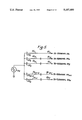
FIG. 1 is a schematic diagram of a neural net layer which embodies the invention, using capacitors to perform weighted summations of synapse signals to be subsequently linearly combined and non-linearly amplified to generate axon response signals.
FIG. 2 is a schematic diagram of a prior art fully differential amplifier and a bias network therefore, as implemented with complementary metal-oxide-semiconductor CMOS field effect transistors, which is useful in the construction of neural nets in accordance with the invention.
FIG. 3 is a schematic diagram of a non-linear voltage amplifier that is useful in the construction of neural nets in accordance with the invention.
FIGS. 4A and 4B together form a FIG. 4 that is a schematic diagram of a modification of the FIG. 1 neural net that can be made manifold times to provide in accordance with a further aspect of the invention, for the programmable weighting of the capacitances used in performing weighted summation of synapse signals.
FIG. 5 is a schematic diagram illustrating one way of pulsing the non-linear output driver amplifiers in a FIG. 1 neural net layer modified manifoldly per FIG. 4.
FIG. 6 is a schematic diagram of a prior-art analog multiplier modified to provide balanced output signals, which is useful in the FIG. 1 neural net modifications shown in FIG. 4 and in FIG. 9.
FIG. 7 is a schematic diagram of training apparatus used with the FIG. 1 neural net layer manifoldly modified per FIG. 4.
FIG. 8 is a schematic diagram of a system having a plurality of neural net layers each constructed in accordance with FIG. 1 modified manifold times per FIG. 4.
FIGS. 9A and 9B together form a FIG. 9 that is a schematic diagram of an alternative modification of the FIG. 1 neural net that can be made manifold times to provide during training for the programmable weighting of the capacitances used in performing weighted summation of synapse signals, in accordance with another aspect of the invention.
FIG. 10 is a schematic diagram of the arrangement of stages in each counter of the FIG. 1 neural net modified per FIG. 9.
FIG. 11 is a schematic diagram of the logic elements included in each counter stage.
FIGS. 12A, 12B and 12C together form a FIG. 12 that is a schematic diagram of further modifications to the neural net, which use pairs of input lines driven by balanced input signals for connection to the pairs of differentially sensed output lines by weighting capacitors connected in bridge configurations.
FIG. 1 shows a neural net comprising a plurality, N in number, of non-linear amplifiers OD1, OD2, . . . OD.sub.(N-1), ODN. Each of a plurality, M in number, of input voltage signals x1, x2, . . . x.sub.(M-1), xM supplied as "synapse" signals is weighted to provide respective input voltages for the non-linear voltage amplifiers OD1, OD2, . . . OD.sub.(N-1), ODN, which generate respective "axon" responses y1, y2, . . . y.sub.(N-1), yN.
M is a positive plural integer indicating the number of input synapse signals to the FIG. 1 net, and N is a positive plural integer indicating the number of output axon signals the FIG. 1 net can generate. To reduce the written material required to describe operation of the FIG. 1 neural net, operations using replicated elements will be described in general terms; using a subscript i ranging over all values one through M for describing operations and apparatuses as they relate to the (column) input signals x1, x2, . . . x.sub.(M-1), xM ; and using a subscript j ranging over all values one through N for describing operations and apparatus as they relate to the (row) output Signals y1, y2, . . . y.sub.(N-1), YN. That is, i and j are the column and row numbers used to describe particular portions of the neural net.
Input voltage signal xi is applied to the input port of an input driver amplifier IDi that is a voltage amplifier which in turn applies its voltage response to an input line ILi. Respective output lines OLj and OL.sub.(j+N) connect to the non-inverting input port of output driver amplifier ODj and to its inverting input port. Output driver amplifier ODj generates at its output port a non-linear voltage response to the cumulative difference in charge on that respective pair of output lines OLj and OL.sub.(j+N).
The non-linear output driver amplifier ODj is shown in FIG. 1 as simply being a differential-input non-linear voltage amplifier with the quiescent direct potential applied to its (+) and (-) input signal terminals via output lines OLj and OL.sub.(j+N) being adjusted by clamping to a desired bias voltage at selected times using a respective direct-current restorer circuit DCRj. The total capacitance of output line OLj to its surroundings and the total capacitance of output line OL.sub.(j+N) to its surroundings are caused to be substantially the same, as will be more particularly described below. A respective capacitor Ci,j connects each of the input lines ILi to each of the output lines OLj, and a respective capacitor Ci,(j+N) connects each of the input lines ILi to each of the output lines OL.sub.(j+N). Since at its output terminal the output driver amplifier ODj responds without inversion to xi input signal voltage applied to its non-inverting (+) input terminal via capacitor Ci,j and responds with inversion to xi input signal voltage applied to its inverting (-) input terminal via capacitor Ci,(j+N), respectively, the electrically equivalent circuit is xi signal voltage being applied to a single output line OLj by a capacitor having a capacitance that equals the capacitance of Ci,j minus the capacitance of Ci,(j+N). This technique of single-ended output signal drive to paired output lines that are differentially sensed avoids the need for switched-capacitance techniques in order to obtain inhibitory (or negative) weights as well as excitory (or positive) weights. Thus this technique facilitates operating the neural net with analog signals that are continuous over sustained periods of time, if so desired.
FIG. 1 shows each of the input lines ILi as being provided with a respective load capacitor CLi to cause that capacitive loading upon the output port of the input driver amplifier IDi to be substantially the same as that upon each output port of the other input driver amplifiers. This is desirable for avoiding unwanted differential delay in responses to the input signals xi. Substantially equal capacitive loading can be achieved by making the capacitance of each of the input line loading capacitors CL1 -CLM very large compared to the total capacitance of the capacitors Ci,j connecting thereto. Preferably, however, this result is achieved by making the capacitance of each of the input line loading capacitors complement the combined value of the other capacitances connecting thereto. This procedure reduces the amount of line loading capacitance required. Where the voltages appearing on the output lines OLj and OL.sub.(j+N) are sensed directly by the non-linear output driver amplifiers OD1, . . . ODN, as shown in FIG. 1, this procedure makes the voltage division ratio for each input voltage x1, . . . xm independent of the voltage division ratios for the other input voltages.
FIG. 1 also shows each of the output lines OLj being loaded with a respective load capacitor CL.sub.(M+j) and each of the output lines OL.sub.(N+j) being loaded with a respective load capacitor CL.sub.(M+N+j). This is done so that the total capacitance on each output line remains substantially the same as on each of the other output lines. This can be done by choosing CL.sub.(M+j) to be much larger than other capacitances to output line OLj, and by choosing CL.sub.(M+N+j) to be much larger than other capacitances to output line OL.sub.(N+j). Alternatively, this can be done by choosing CL.sub.(M+j) and CL.sub.(M+N+j) to complement the combined value of the other capacitances connecting the same output line. The input voltage to output driver amplifier ODj will (to good approximation) have the following value, vj, in accordance with Coulomb's Law. ##EQU6## The generation of voltage vj can be viewed as the superposition of a plurality of capacitive divisions between, on the one hand, the effective capacitance (C.sub.(i,j) -Ci,(j+N)) each input voltage has to output line OLj and, on the other hand, the total capacitance Cj of the output line to its surroundings. That is, Cj is the total capacitance on output line OLj or the total capacitance on output line OL.sub.(N+j), which capacitances should be equal to each other and fixed in value. Where the difference in charge appearing on the output lines OLj and OL.sub.(j+N) is sensed by fully differential charge-sensing amplifiers preceding the non-linear voltage amplifiers in the output driver amplifiers, as will be described later on in this specification in connection with FIG. 4, the output signals from the charge-sensing amplifiers will be balanced with reference to a reference VBIAS potential.
FIG. 2 shows a fully differential amplifier constructed of MOS field-effect transistors Q1 -Q13, as may serve for any one of the fully differential amplifiers DAj for j=1, 2, . . . N. Also shown is a bias network constructed of MOS field effect transistors Q14 -Q19 for generating direct bias potentials for application to that fully differential amplifier and to others of its kind. This circuitry is described in more detail on pages 255-257 of the book Analog MOS Integrated Circuits for Signal Processing by R. Gregorian and G.C. Temes, copyright 1986, published by John Wiley & Sons, Inc., of New York, Chichester, Brisbane, Toronto and Singapore.
The fully differential amplifier includes a long-tailed-pair connection of n-channel MOSFETs Q1 and Q2 providing common-mode rejection for the input voltages IN and IN applied to the (+) and (-) input terminals at their respective gate electrodes. N-channel MOSFET Q13 is connected as a constant-current sink for tail current from the interconnection between the source electrodes of Q1 and QL. Q1 and Q2 are in folded cascade connections with p-channel MOSFETs Q7 and Q8 respectively. There is also common mode rejection for output voltages OUT and OUT appearing at the (+) and (-) output terminals connecting from the drain electrodes of Q7 and Q8 respectively, which is why the differential amplifier comprising Q1 -Q13 is described as being "fully" differential. This common mode rejection is provided by common-mode degenerative feedback connections from the (-) and (+) output terminals to the gate electrodes of p-channel MOSFETs Q3 and Q4, the paralleled source-to-drain paths of which supply current to the joined source electrodes of p-channel MOSFETs Q5 and Q6 operated as a current splitter. Q5 drain current biases the folded cascode connection of Q1 and Q7, and Q6 drain current biases the folded cascode connection of Q2 and Q8. N-channel MOSFETs Q9 and Q11 are in a cascode connection biased to provide a high-impedance constant-current sink as drain load to Q7, and n-channel MOSFETs Q10 and Q12 are in a cascode connection biased to provide a high-impedance constant-current sink as drain load to Q8.
The (+) and (-) output terminals can be biased to the same (+2.5 v) potential as applied to the gate electrode of MOSFET Q14 by causing MOSFETs Q1 -Q18 to have the following width-to-length ratios presuming Q1, Q2, Q7 and Q8 to have equal amplitude quiescent channel currents.
______________________________________
(W/L).sub.11 :(W/L).sub.12 :(W/L).sub.13 :(W/L).sub.18 ::2:2:1:1
                             (6)
(W/L).sub.3 :(W/L).sub.4 :(W/L).sub.14 ::1:1:1
                             (7)
(W/L).sub.5 :(W/L).sub.6 :(W/L).sub.15 ::1:1:1
                             (8)
(W/L).sub.7 :(W/L).sub.8 :(W/L).sub.16 ::2:2:1
                             (9)
(W/L).sub.9 :(W/L).sub.10 :(W/L).sub.17 ::2:2:1
                            (10)
______________________________________
The width-to-length ratio of MOSFET Q19 is chosen to provide responsive to the drain current demand of Q14 a voltage drop across Q19 channel that affords sufficient operating voltage range for signals at terminals out and OUT.
FIG. 3 shows non-linear voltage amplifier circuitry that can be used after linear voltage amplifier circuitry to implement each non-linear output driver amplifier ODj in the FIG. 1 neural net layer. The FIG. 3 non-linear voltage amplifier is a cascade connection of two source-follower transistors, one (Q20A) being an n-channel MOSFET and the other (Q20B) being a p-channel MOSFET. Q20A is provided a constant-current generator source load by an n-channel MOSFET Q21, which is the slave or output transistor of a current mirror amplifier including as its master or input transistor an n-channel MOSFET Q22 self-biased by drain-to-gate feedback. Q20B is provided a constant-current generator source load by a p-channel MOSFET Q23, which is the slave or output transistor of a current mirror amplifier including as its master or input transistor a p-channel MOSFET Q24 self-biased by drain-to-gate feedback. Q22 and Q24 are connected as diodes by their respective drain-to-gate feedback connections, and these diodes are connected in series with another diode-connected n-channel MOSFET Q25 and with another diode-connected p-channel MOSFET Q26 between VSS and VDD potentials to implement a bias network. In this bias network a quiescent input current flows from the input port of the current mirror amplifier comprising Q23, Q24 into the input port of the current mirror amplifier comprising Q21, Q22. Q21 and Q23 drain current flows are similar-valued by current mirror amplifier action.
All the n-channel MOSFETs Q20A, Q21, Q22 and Q25 have similar channel widths and lengths and exhibit similar operating characteristics. All the p-channel MOSFETs Q20B, Q23, Q24 and Q26 have similar channel widths and lengths and exhibit similar operating characteristics, which are complementary to those of the n-channel MOSFETs. The bias network MOSFETs Q22, Q24, Q25 and Q26 may be shared by a plurality of the FIG. 3 non-linear voltage amplifier circuits to conserve hardware and operating power.
Non-linearity of response in the FIG. 3 voltage amplifier comes about because (1) source-follower action of Q20A for positive-going excursions of its gate electrode potential becomes limited as its source potential approaches its drain potential VHI and (2) source-follower action of Q20 for negative-going excursions of its gate electrode potential becomes limited as its source potential approaches its drain potential VLO. At the source electrode of source-follower Q20B there is a sigmoidal response to a linear ramp potential applied to the gate electrode of source-follower Q20A. The voltages VLO and VHI can be programmed to control the limiting properties of the FIG. 3 non-linear amplifier, and the voltages VLO and VHI may be selected to provide for symmetry of response or for asymmetry of response. FIG. 3 shows representative values for VHI and VLO that provide a substantially symmetrical response about +2.5 volts.
Output driver amplifier ODj can use non-linear voltage amplifier circuitry different from that shown in FIG. 3. For example, source followers Q20A and Q20B can be reversed in order of their cascade connection. Either this alternative circuitry or the FIG. 3 circuitry can be preceded by a charge-sensing amplifier, rather than a linear voltage amplifier, to realize the type of output driver amplifier used in FIG. 4 and FIG. 9 neural nets. In the FIG. 1 neural net the output driver amplifiers can be realized without using the FIG. 3 circuitry or the previously described alternative circuitry. For example, each output driver amplifier can comprise a long-tailed pair connection of transistors having a current mirror amplifier load for converting their output signal voltage to single-ended form. The long-tailed pair connection of transistors is a differential amplifier connection where their source electrodes have a differential-mode connection to each other and to a constant-current generator.
Consider now how neuron model behavior is exhibited by input driver amplifier IDi, capacitors Ci,j and Ci,(j+N), and non-linear output driver amplifier ODj for particular respective values of i and j. If the capacitance of capacitor Ci,j is larger than the capacitance of capacitor Ci,(j+N) for these particular values of i and j, then the output voltage yj for that j will exhibit "excitory" response to the input voltage xi. If the capacitances of Ci,j and Ci,(j+N) are equal for these i and j values, then the output voltage yj for that j should exhibit no response to the input voltage yj. If the capacitance of capacitor Ci,j is smaller than the capacitance of capacitor Ci(j+N) for those i and j values, then the output voltage yj for that j will exhibit "inhibitory" response to the input voltage xi.
In some neural nets constructed in accordance with the invention the capacitors Ci,j and Ci,(j+N) for all i and j may be fixed-value capacitors, so there is never any alteration in the weighting of input voltages xi where i=1,. . . M. However, such neural nets lack the capacity to adapt to changing criteria for neural responses--which adaptation is necessary, for example, in a neural network that is to be connected for self-learning. It is desirable in certain applications, then, to provide for altering the capacitances of each pair of capacitors Ci,j and Ci,(j+N) associated with a respective pair of values of i and j. This alteration is to be carried out in a complementary way, so the sum of the capacitances of Ci,j and of Ci(j+N) remains equal to Ck. For example, this can be implemented along the lines of the inventor's previous teachings in regard to "digital" capacitors, having capacitances controlled in proportion to binary-numbers used as control signals, as particularly disclosed in connection with FIG. 11 of his U.S. Pat. No. 3,890,635 issued Jun. 17, 1975, entitled "VARIABLE CAPACITANCE SEMICONDUCTOR DEVICES" and assigned to General Electric Company. Each pair of capacitors Ci,j and Ci,j+N) is then two similar ones of these capacitors and their capacitances are controlled by respective control signals, one of which is the one's complement of the other.
Alternatively, the pair of capacitors Ci,j and Ci,(j+N) may be formed from selecting each of a set of component capacitors with capacitances related in accordance with powers of two to be a component of one or the other of the pair of capacitors Ci,j and Ci(j+N), the selecting being done by field effect transistors (FETs) operated as transmission gates. Yet another way of realizing the pair of capacitors Ci,j and Ci,(j+N) is to control the inverted surface potentials of a pair of similar size metal-oxide-semiconductor (MOS) capacitors with respective analog signals developed by digital-to-analog conversion.
FIG. 4, comprising component FIGS. 4A and 4B, shows a representative modification that can be made to the FIG. 1 neural net near each set of intersections of an output lines OLj and OLj+N) with an input line ILi from which they receive with differential weighting a synapse input signal xi. Such modifications together make the neural net capable of being trained. Each capacitor pair Ci,j and Ci,(j+N) of the FIG. 1 neural net is to be provided by a pair of digital capacitors DCi,j and DCi,(j+N). (For example, each of these capacitors DCi,j and DCi,(j+N) may be as shown in FIG. 11 of U.S. Pat. No. 3,890,635). The capacitances of DCi,j and DCi,(j+N) are controlled in complementary ways by a digital word and its one's complement, as drawn from a respective word-storage element WSEi,j in an array of such elements located interstitially among the rows of digital capacitors and connected to form a memory. This memory may, for example, be a random access memory (RAM) with each word-storage element WSEi,j being selectively addressable by row and column address lines controlled by address decoders. Or, by way of further example, this memory can be a plurality of static shift registers, one for each column j. Each static shift register will then have a respective stage WSEi,j for storing the word that controls the capacitances of each pair of digital capacitors DCi,j and DCi,(j+N).
The word stored in word storage element WSEi,j may also control the capacitances of a further pair of digital capacitors DC.sub.(i+M),j and DC.sub.(i+M),(j+N), respectively. The capacitors DC.sub.(i+M),j and DC.sub.(i+M),(j+N) connect between "ac ground" and output lines OLj and OL.sub.(j+N), respectively, and form parts of the loading capacitors CL.sub.(M+j). The capacitances of DC.sub.(i+2M,j) and DCi,j are similar to each other and changes in their respective values track each other. The capacitances of DC.sub.(i+M),(j+N) and DCi,(j+N) are similar to each other and changes in their respective values track each other. The four digital capacitors DCi,j, DCi,(j+N), DC.sub.(i+M),j and DC.sub.(ik+M),(j+N) are connected in a bridge configuration having input terminals connecting from the input line ILi and from a-c ground respectively and having output terminals connecting to output lines OLj and OL.sub.(j+N) respectively. This bridge configuration facilitates making computations associated with back-propagation programming by helping make the capacitance network bilateral insofar as voltage gain is concerned. Alternatively, where the computations for back-propagation programming are done by computers that do not involve the neural net in the computation procedures, the neural net need not include the digital capacitors DC.sub.(i+M),j and DC.sub.(i+M),(j+N).
When the FIG. 4 neural net is being operated normally, following programming, the φP signal applied to a mode control line MCL is a logic ZERO. This ZERO on mode control line MCL conditions each output line multiplexer OLMj of an N-numbered plurality thereof to select the output line OLj to the inverting input terminal of a respective associated fully differential amplifier DAj. This ZERO on mode control line MCL also conditions each output line multiplexer OLMj+N) to select the output line OLj+N) to the non-inverting input terminal of the respective associated fully differential amplifier DAj. Differential amplifier DAj, which may be of the form shown in FIG. 2, is included in a respective charge-sensing amplifier QSj that performs a charge-sensing operation for output line OLj. In furtherance of this charge-sensing operation, a transmission gate TGj responds to the absence of a reset pulse QR to connect an integrating capacitor CIj between the (+) output and (-) input terminals of amplifier DAj ; and a transmission gate TG.sub.(j+5N) responds to the absence of the reset pulse φR to connect an integrating capacitor CI.sub.(j+N) between the (-) output and (+) input terminals of amplifier DAj. With integrating capacitors CIj and CI.sub.(j+N) so connected, amplifier DAj functions as a differential charge amplifier. When φp signal on mode control line MCL is a ZERO, the input signal xi induces a total differential change in charge on the capacitors DCi,j and DCi,(j+N) proportional to the difference in their respective capacitances. The resulting displacement current flows needed to keep the input terminals of differential amplifier DAj substantially equal in potential requires that there be corresponding displacement current flow from the integrating capacitor CIj and CI.sub.(j+N) differentially charging those charging capacitors to place thereacross a differential voltage vj defined as follows. ##EQU7##
The half Vj signal from the non-inverting (+) output terminal of amplifier DAj is supplied to a non-linear voltage amplifier circuit NLj which can be the non-linear voltage amplifier circuit of FIG. 3 or an alternative circuit as previously described. If the alternative non-linear voltage amplifier circuit is one adapted for receiving push-pull input voltages, such as the non-linear long-tailed pair connection of transistors supplying a balanced-to-single-ended converter previously alluded to, it may receive both the +vj and -vj output voltages from the differential charge-sensing amplifier DSQj as its push-pull input voltages. The FIG. 3 non-linear voltage amplifier circuit does not require the -vj output voltage from the differential charge-sensing amplifier DSQj as an input voltage, so this output of the differential charge-sensing amplifier DSQj is shown in FIG. 4A as being left unconnected to further circuitry. The non-linear voltage amplifier circuit NLj responds to generate the axon output response yj. It is presumed that this non-linear voltage amplifier NLj supplies yj at a relatively low source impedance as compared to the input impedance offered by the circuit yj is to be supplied to--e.g. on input line in a succeeding neural net layer. If this is so there is no need in a succeeding neural net layer to interpose an input driver amplifier IDi as shown in FIG. 1. This facilitates interconnections between successive neural net layers being bilateral. An output line multiplexer OLMj responds to the φP signal appearing on the mode control line MCL being ZERO to apply yj to an input line of a succeeding neural net layer if the elements shown in FIG. 4 are in a hidden layer. If the elements shown in FIG. 4 are in the output neural net layer, output line multiplexer OLMj responds to the φP signal on the mode control line being ZERO to apply yj to an output terminal for the neural net.
From time to time, the normal operation of the neural net is interrupted; and, to implement dc-restoration a reset pulse φR is supplied to the charge sensing amplifier QSj. Responsive to φR, the logic complement of the reset pulse φR, going low when φR goes high, transmission gates TGj and TG.sub.(j+SN) are no longer rendered conductive to connect the integrating capacitors CIj and CI.sub.(j+N) from the output terminals of differential amplifier Daj. Instead, transmission gates TG.sub.(j+N) and TG.sub.(j+4N) respond to φR going high to connect to VBIAS the plates of capacitor CIj and CI.sub.(j+N) normally connected from those output terminals, VBIAS being the 2.5 volt intermediate potential between the VSS =0 volt and VDD =5 volt operating voltages of differential amplifier Daj. Other transmission gates TG.sub.(j+2N) and TG.sub.(J+3N) respond to φR going high to apply direct-coupled degenerative feedback from the output terminal of differential amplifier DAj to its input terminals, to bring the voltage at the output terminals to that supplied to its inverting input terminal from output lines OLj and OL.sub.(j+N). During the dc-restoration all xi are "zero-valued". So the charges on integrating capacitor CIj and CI.sub.(j+N) are adjusted to compensate for any differential direct voltage error occurring in the circuitry up to the output terminals of differential amplifier Daj. Dc-restoration is done concurrently for all differential amplifiers DAj (i.e., for values of j ranging from one to N).
During training, the φP signal applied to mode control line MCL is a logic ONE, which causes the output line multiplexer OLMj to disconnect the output lines OLj and OL.sub.(j+N) from the (+) and (-) input terminals of differential amplifier DAj and to connect the output lines OLj and OL.sub.(j+N) to receive +δj and -δj error terms. These +δj and -δj error terms are generated as the balanced product output signal of a analog multiplier AMj, responsive to a signal Δj and to a signal y'j which is the change in output voltage yj of non-linear amplifier NLj for unit change in the voltage on output line OLj. The term Δj for the output neural net layer is an error signal that is the difference between yj actual value and its desired value dj. The term Δj for a hidden neural net layer is also an error signal, which is of a nature that will be explained in detail further on in this specification.
Differentiator DFj generates the signal y'j, which is a derivative indicative of the slope of yj change in voltage on output line OLj, superposed on VBIAS. To determine the y'j derivative, a pulse doublet comprising a small positive-going pulse immediately followed by a similar-amplitude negative-going pulse is introduced at the inverting input terminal of differential amplifier DAj (or equivalently, the opposite-polarity doublet pulse is introduced at the non-inverting input terminal of differential amplifier DAj) to first lower yj slightly below normal value and then raise it slightly above normal value. This transition of yj from slightly below normal value to slightly above normal value is applied via a differentiating capacitor CDj to differentiator DFj.
Differentiator DFj includes a charge sensing amplifier including a differential amplifier DA.sub.(j+N) and an integrating capacitor CI.sub.(j+N). During the time yj that is slightly below normal value, a reset pulse φS is applied to transmission gates TG.sub.(j+4N) and TG.sub.(j+5N) to render them conductive. This is done to drain charge from integrating capacitor CI.sub.(J+N), except for that charge needed to compensate for DA.sub.(j+N) input offset voltage error. The reset pulse φS ends, rendering transmission gates TGB.sub.(j+4N) and TG.sub.(j+5N) no longer conductive, and the complementary signal φS goes high to render a transmission gate TG.sub.(j+3N) conductive for connecting integrating capacitor CI.sub.(j+N) between the output and inverting-input terminals of differential amplifier DA.sub.(j+N).
With the charge-sensing amplifier Comprising elements DA.sub.(j+N) and CI.sub.(j+N) reset, the small downward pulsing of yj from normal value is discontinued and the small upward pulsing of yj from normal value occurs. The transition between the two abnormal conditions of yj is applied to the charge-sensing amplifier by electrostatic induction via differentiating capacitor CDj. Differential amplifier DA.sub.(j+N) output voltage changes by an amount y'j from the VBIAS value it assumed during reset. The use of the transition between the two pulses of the doublet, rather than the edge of a singlet pulse, to determine the derivative y'j makes the derivative-taking process treat more similarly those excitory and inhibiting responses of the same amplitude. The doublet pulse introduces no direct potential offset error into the neural net layer.
Responsive to a pulse φT, the value y'j+V BIAS from differentiator DFj is sampled and held by row sample and hold circuit RSHj for application to analog multiplier AMj as an input signal. This sample and hold procedure allows yj to return to its normal value, which is useful in the output layer to facilitate providing yj for calculating (yj -dj). The sample and hold circuit RSHj may simply comprise an L-section with a series-arm transmission-gate sample switch and a shunt-leg hold capacitor, for example. Analog multiplier AMj is of a type accepting differential input signals, as will be described in greater detail further on in connection with FIG. 6. The difference between y'j +VBIAS and VBIAS voltages is used as a differential input signal to analog multiplier AMj, which exhibits common-mode rejection for the VBIAS term.
During training, the φP signal applied to mode control line MCL is a logic ONE, as previously noted. When the FIG. 4 elements are in the output layer, the ONE on mode control line MCL conditions an output multiplexer OMj to discontinue the application of yj signal from non-linear amplifier NLj to an output terminal. Instead, the output multiplexer OMj connects the output terminal to a charge-sensing amplifier QSj. Charge sensing amplifier QSj includes a differential amplifier DA.sub.(j+2N) and an integrating capacitor CI.sub.(j+2N) and is periodically reset responsive to a reset pulse φU. Reset pulse φU can occur simultaneously with reset pulse φS, for example. Output signal Δj from charge-sensing amplifier QSj is not used in the output layer, however. Analog multiplier AMj does not use Δj +VBIAS and VBIAS as a differential input signal in the output layer, (yj -dj) being used instead.
When the FIG. 4 elements are in a hidden neural net layer, φP signal on the mode control line MCL being a ONE conditions output multiplexer OMj to discontinue the application of yj signal from non-linear amplifier NLj to the input line ILj of the next neural net layer. Instead, output multiplexer OMj connects the input line ILj to a charge-sensing amplifier QSj. Charge-sensing amplifier QSj senses change in the charge on input line ILj during training to develop a Δj error signal superposed on VBIAS direct potential. The difference between Δj +VBIAS and VBIAS voltages is used as a differential input signal to analog multiplier AMj, which multiplier exhibits common-mode rejection for the VBIAS term.
Charge-sensing amplifier QSj employs a differential-input amplifier DA.sub.(j+2N) and an integrating capacitor CI.sub.(j+2N). Transmission gates TG.sub.(j+9N), TG.sub.(j+10N) and TG.sub.(j+11N) cooperate to provide occasional resetting of charge conditions on the integrating capacitor CIj+2N responsive to the reset pulse φU.
FIG. 5 shows how each output line OLj for j=1, . . . N may be pulsed during calculation of y'j terms. Each output line OLj is connected by a respective capacitor COj to the output terminal of a pulse generator PG, which generates the doublet pulse. FIG. 5 shows the doublet pulse applied to the end of each output line OLj remote from the--terminal of the associated differential amplifier DAj in the charge-sensing amplifier QSj sensing the charge on that line. It is also possible to apply the doublet pulses more directly to those--terminals by connecting to these terminals respective ones of the plates of capacitors COj that are remote from the plates connecting to pulse generator PG.
Each output line OLj has a respective capacitor COj connected between it and a point of reference potential, and each output line OL.sub.(j+N) has a respective capacitor CO.sub.(j+N) connected between it and a point of reference potential, which capacitors are not shown in the drawing. The respective capacitances of the capacitors COj and CO.sub.(j+N) are all of the same value, so that the back-propagation algorithm is not affected by the presence of these capacitors. Arrangements for adding the doublet pulse to vj before its application to the non-linear amplifier NLj can be used, rather than using the FIG. 5 arrangement.
FIG. 6 shows a four-quadrant analog multiplier supplying product output signal in balanced form at its output terminals POUT and POUT. It is a modification of a single-ended-output analog multiplier described by K. Bultt and H. Wallinga in their paper "A CMOS Four-quadrant Analog Multiplier" appearing on pages 430-435 of the IEEE JOURNAL OF SOLID STATE CIRCUITS, Vol. SC-21, No. 3, June. 1986, incorporated herein by reference. The FIG. 6 analog multiplier accepts a first push-pull input signal between input terminals and IN1 and IN1, and it accepts a second push-put pull input signal between terminals IN2 and IN2.
As described by Bultt and Wallinga there are four component analog multipliers: a first comprising n-channel MOSFETs Q27 -Q29, a second comprising n-channel MOSFETs Q30 -Q32, a third comprising n-channel MOSFETs Q33 Q35 and a fourth comprises n-channel MOSFETs Q36 -Q38. The component analog multipliers are arranged in cross-coupled pairs to suppress quadratic and offset terms. Constant-current generator IGI provides for floating of the potentials at input terminals IN1 and IN1, and constant-current generator IG2 provides for floating of the potentials at input terminals IN2 and IN2. The push-pull outputs of the four-quadrant analog multiplier are supplied to diode-connected p-channel MOSFETs Q39 and Q40, which are the master or input transistors of respective current mirror amplifiers., Q39 and Q40 have respective p-channel MOS slave or output transistors Q41 and Q42 associated with them in their respective current mirror amplifiers, and as in the Bultt and Wallinga analog multiplier the push-pull variations in the drain currents of Q41 and Q42 are converted to single-ended form at output terminal POUT using a current mirror amplifier connection of n-channel MOSFETs Q43 and Q44. In FIG. 6 Q39 and Q40 additionally have respective further p-channel MOS slave or output transistors Q45 and Q46 associated with them in their respective current mirror amplifiers, which are dual-output rather than single-output in nature. The push-pull variations in the drain currents of Q45 and Q46 are converted to single-ended form at terminal POUT using a current mirror amplifier connection of n-channel MOSFETs Q47 and Q48. Since the current mirror amplifier connections of Q43 and Q47 are driven push-pull, the output signals at output terminals POUT and POUT exhibit variations in opposite senses of swing.
FIG. 7 shows apparatuses for completing the back-propagation computations, as may be used with the FIG. 1 neural net manifoldly modified per FIG. 4. The weights at each word storage element WSEi,j in the interstitial memory array IMA are to be adjusted as the i column addresses and j row addresses are scanned row by row, one column at a time. An address scanning generator ASG generates this scan of i and j addresses shown applied to interstitial memory array IMA, assuming it to be a random access memory. The row address j is applied to a row multiplexer RM that selects δj to one input of a multiplier MULT, and the column address i is applied to a column multiplexer CM that selects xi to another input of the multiplier MULT.
Multiplier MULT is of a type providing a digital output responsive to the product of its analog input signals. Multiplier MULT may be a multiplying analog-to-digital converter, or it may comprise an analog multiplier followed by an analog-to-digital converter, or it may comprise an analog-to-digital converter for each of its input signals and a digital multiplier for multiplying together the converted signals. Multiplier MULT generates the product xi δj as reduced by a scaling factor η, which is the increment or decrement to the weight stored in the currently addressed word storage element WSEij in the memory array IMA. The former value of weight stored in word storage element WSEij is read from memory array IMA to a temporary storage element, or latch, TS. This former weight value is supplied as minuend to a digital subtractor SUB, which receives as subtrahend η xi δj from multiplier MULT. The resulting difference is the updated weight value which is written into word storage element WSEi,j in memory array IMA to replace the former weight value.
FIG. 8 shows how trained neural net layers L0, L1 and L2 are connected together in a system that can be trained. L0 is the output neural net layer that generates yj output signals, is similar to that described in connection with FIGS. 4 and 5, and is provided with a back-propagation processor BPP0 with elements similar to those shown in FIG. 7 for updating the weights stored in the interstitial memory array of L0. L1 is the first hidden neural net layer which generates yi output signals Supplied to the output neural net layer as its xi input signals. These yi output signals are generated by layer L1 as its non-linear response to the weighted sum of its xh input signals. This first hidden neural net layer L1 is provided with a back-propagation processor BPP1 similar to BPP0. L2 is the second hidden neural net layer, which generates yh output signals supplied to the first hidden neural net layer as its x.sub. h input signals. These yh output signals are generated by layer L2 as its non-linear response to a weighted summation of its xg input signals. This second hidden layer is provided with a back-propagation processor similar to BPP0 and to BPP1.
FIG. 8 presumes that the respective interstitial memory array IMA of each neural net layer L0, L1, L2 has a combined read/write bus instead of separate read input and write output busses as shown in FIG. 7. FIG. 8 shows the Δj, Δi and Δh signals being fed back over paths separate from the feed forward paths for yj, yi and yh signals, which separate paths are shown to simplify conceptualization of the neural net by the reader. In actuality, as shown in FIGS. 4 and 9, a single path may be used to transmit yj in the forward direction and Δj in the reverse direction, etc. Back-propagation processor BPP0 modifies the weights read from word storage elements in neural net layer L0 interstitial memory array by ηxi δj amounts and writes them back to the word storage elements in a sequence of read-modify-write cycles during the training procedure. Back-propagation processor BPP1 modifies the weights read from word storage elements in neural net layer L1 interstitial memory array by ηxh δi amounts and writes them back to the word storage elements in a sequence of read-modify-write cycles, during the training procedure. Back-propagation processor BPP2 modifies the weights read and storage elements in neural net layer L2 interstitial memory array by ηxg δh amounts and writes them back to the word storage element in a sequence of read-modify-write cycles during the training procedure.
FIG. 9, comprising component FIGS. 9A and 9B shows an alternative modification that can be manifoldly made to the FIG. 1 neural net layer to give it training capability. This alternative modification seeks to avoid the need for a high-resolution multiplier MULT and complex addressing during back-propagation calculations in order that training can be implemented. A respective up/down counter UDCi,j is used instead of each word storage element WSEi,j. Correction of the word stored in counter UDCi,j is done a count at a time; and the counter preferably has at least one higher resolution stage in addition to those used to control the capacitances of digital capacitors DCi,j, DC.sub.(i+M),j, DCi,(j+N) and DC.sub.(i+M),(j+N). Each up/down counter UDCi,j has a respective counter control circuit CONi,j associated therewith. Each counter control circuit CONi,j may, as shown in FIG. 9a, and described in detail further on in this specification simply consist of an exclusive-OR gate XORi,j.
A row sign detector RSDj detects whether the polarity of δj is positive or negative, indicative of whether a row of weights should in general be decremented or incremented, and broadcasts its detection result via a row sign line RSLj to all counter control circuits (CONi,j for i=1, . . . , M) in the row j associated with that row sign detector RSDj. Before making a back-propagation calculation, a respective column sign detector CSDi detects whether the polarity of xi is positive or negative for each columnar position along the row which is to be updated, to provide an indication of whether it is likely the associated weight should be decremented or incremented. This indication is stored temporarily in a (column) sample and hold circuit CSHi. Each column sample and hold circuit CSHi is connected to broadcast its estimate via a column sign line CSLi to all counter control circuits (CONi,j for j=1, . . . N) in the column i associated with that sample and hold circuit CSH.sub. i. Responsive to these indications from sign detectors CSDi and RSDj, each respective counter control circuit CONi,j decides in which direction up/down counter UDCi,j will count to adjust the weight control signals Di,j and Di,j stored therein
The counter control circuitry CONi,j should respond to the sign of +δj being positive, indicating the response vj to be too positive, to decrease the capacitance to output line OLj that is associated with the signal xi or -xi that is positive and to increase the capacitance to output line OLj that is associated with the signal -xi or xi that is negative, for each value of i. The counter control circuitry CONi,j should respond to the sign of +δj being negative, indicating the response v to be too negative, to increase the capacitance to output line OLj that is associated with the signal -xi or xi that is negative and to decrease the capacitance to output line OLj that is associated with the signal xi or -xi that is positive. Accordingly, counter control circuitry CONi,j may simply consist of a respective exclusive-OR gate XORi,j as shown in FIG. 9a, if the following presumptions are valid.
Each of the digital capacitors DCi,j and DC.sub.(i+M),(j+N) is presumed to increase or decrease its capacitance as Di,j is increased or decreased respectively. Each of the digital capacitors DC.sub.(i+M),j and DCi,(j+N) is presumed to increase or decrease its capacitance as Di,j is increased or decreased respectively. A ZERO applied as up/down signal to up/down counter UDCi,j is presumed to cause counting down for Di,j and counting up for Di,j. A ONE applied as up/down signal to up/down counter UDCi,j is presumed to cause counting up for Di,j and counting down for i,j. Column sign detector CSDi output indication is presumed to be a ZERO when xi is not negative and to be a ONE when xi is negative. Row sign detector RSDj output indication is presumed to be a ZERO when δj is not negative and to be a ONE when δj is negative. Since the condition where xi or δj is zero-valued is treated as if the zero-valued number were positive, forcing a false correction which is in fact not necessary, and thus usually creating the need for a counter-correction in the next cycle of back-propagation training, there is dither in the correction loops. However, the extra stage or stages of resolution in each up/down counter UDCi,j prevent high-resolution dither in the feedback correction loop affecting the capacitances of DCi,j, DC.sub.(i+M),j, DCi,(j+N) and DC.sub.(i+M),(j+N).
Analog multiplier AMj develops balanced product signals, +δj and -δj , that can be supplied to a voltage comparator that serves as the row sign detector RSDj. Alternatively, since the derivative y'j always has the same sign (normally a positive one), one can use a voltage comparator to compare the voltages supplied to input terminals of analog multiplier Aamj the other than those which receive y'j +VBIAS and VBIAS for providing the row sign detector RSDj its input signal.
FIG. 10 shows the construction of counter UDCi,j being one that has a plurality of binary counter stages BCS1, BCS2, BCS3 that provide increasingly more significant bits of the weight control signal Di,j and of its one's complement Di,j. FIG. 11 shows the logic within each binary counter stage which is implemented with MOS circuitry that is conventional in the art. FIGS. 10 and 11 make it clear that the opposite directions of counting for Di,j and Di,j can be controlled responsive to a ZERO or ONE up/down control signal in either of two ways, depending on whether Di,j is taken from Q outputs of the flip-flops and Di,j is taken from their Q outputs, as shown, or whether Di,j is taken from the Q outputs of the flip-flops and Di,j is taken from their Q outputs. If the latter choice had been made instead, each counter control circuit CONi,j would have to consist of a respective exclusive-NOR circuit, or alternatively the CSDi and RSDj sign detectors would have to be of opposite logic types, rather than of same logic type.
FIG. 12 comprising FIGS. 12A, 12B and 12C shows further modification that can be made to the FIG. 9 modification for the FIG. 1 neural net. This modification, as shown in FIG. 12A provides for a pair of input lines ILi and IL.sub.(i+M) for driving each bridge configuration of digital capacitors DCi,j, DCi,(j+N), DC.sub.(i+M),j and DC.sub.(i+M),(j+N) push-pull rather than single-ended. Push-pull, rather than single-ended drive is provided to the differential charge sensing amplifier DQSj, doubling its output response voltage. Push-pull drive also permits differential charge sensing amplifier DSQj to be realized with differential-input amplifiers that do not provide for common-mode suppression of their output signals, if one so desires. FIG. 12A differs from FIG. 9A in that sign detector CSDi and CSHi do not appear, being relocated to appear in FIG. 12C as shall be considered further later on.
FIG. 12B differs from FIG. 9B in that the single-ended charge-sensing amplifier QSi does not appear, being inappropriate for sensing differences in charge appearing on a pair of input lines. Instead, δj +BBIAS is developed in the following neural net layer and is fed back to analog multiplier AMj via the output multiplexer OMj when the φp signal on mode control line MCL is a ONE.
FIG. 12C shows circuitry that may be used in each neural net layer to provide balanced input signal drive to a pair of input lines ILi and IL.sub.(i+M) during normal operation and to differentially sense the charge on those input lines during back-propagation calculations. A single fully differential amplifier IDi, which is by way of example of the type shown in FIG. 2, is multiplexed to implement both functions in duplex circuitry DPXi shown in FIG. 12C. Alternatively the functions could be implemented with separate apparatus.
During normal operation the φP signal appearing on mode control line MCL is a ZERO, conditioning an input multiplexer IMi to apply xi signal to the non-inverting (+) input terminal of differential amplifier IDi and conditioning input line multiplexers ILMi and ILM.sub.(i+M) to connect the non-inverting (+) and inverting (-) output terminals of differential amplifier IDi to input lines ILi and IL.sub.(i+M) respectively. A sign θP is a ONE during normal operation and appears in the φU +φP control signal applied to a transmission gate between the non-inverting (+) output terminal of differential amplifier IDi and its inverting (-) input terminal, rendering that transmission gate conductive to provide direct-coupled feedback between those terminals. This d-c feedback conditions differential amplifier IDi to provide xi and -xi responses at its (+) and (-) output terminals to the xi signal applied to its (-) input terminal. Other transmission gates within the duplex circuitry DPXi are conditioned to be non-conductive during normal operation.
During back-propagation calculations, the φP signal appearing on mode control line MCL is a ONE, conditioning input multiplexer IMi to apply Δi signal from the non-inverting (+) output terminal of differential amplifier IDi to the preceding neural net layer, if any, and conditioning input line multiplexers ILMi and ILM--(i+M) to connect the input lines ILi and IL.sub.(i+M) to respective ones of the non-inverting (+) and inverting (-) input terminals of differential amplifier IDi. Integrating capacitors ICi and IC.sub.(i+M) connect from the (+) and (-) output terminals of differential amplifier IDi to its (-) and (+) input terminals when transmission gates in duplex circuitry DPXi that are controlled by φU ·φP signal receive a ZERO during back-propagation calculations. The charge conditions on integrating capacitors ICi and IC.sub.(i+M) are reset when φU occasionally pulses to ONE during back-propagation calculations. This happens in response to transmission gates in duplexer Circuitry DpXi receptive of φU and φU +φP control signals being rendered conductive responsive to φu being momentarily a ONE, while transmission gates in duplexer circuitry DPXi receptive of φU control signal being rendered non-conductive.
Column sign detector CSDi and column sample and hold circuit CSHi appear in FIG. 12C. Column sign detector receives output signal from differential amplifier IDi directly as its input signal and can simply be a voltage comparator for the xi and -xi output signals from the differential amplifier IDi.
The multiplexers employed in various portions of the circuits described above are customarily constructed of single-pole switch elements, each of which single-pole switch elements is conventionally a so-called "transmission gate" connection of one or more field effect transistors in CMOS design. A suitable transmission gate is provided by the paralleled channels of a p-channel FET and an n-channel FET having oppositely swinging control voltages applied to their respective gate electrodes to control the selective conduction of those paralleled channels.
In U.S. Pat. No. 4,950,917 issued Aug. 21, 1990 and entitled "SEMICONDUCTOR CELL FOR NEURAL NETWORK EMPLOYING A FOUR-QUADRANT MULTIPLIER" M.A. Holler, S.M. Tam, R.G. Benson and H.A. Castro describe using MOSFET transconductance multipliers for the weighting of synapse input signals prior to summation. The use of MOSFET transconductance multipliers for the weighting of synapse input signals prior to summation is also described by S. Bibyk and M. Ismail in the fifth chapter "Issues in Analog VSI and MOS Techniques for Neural Computing" on pages 104-133 of a book Analog VLSI Implementation of Neural Systems edited by C. Mead et alii and published by Kluwer Academic Publishers, Norwell MA, copyright 1989. The conductances presented by the MOSFETs in these transconductance multipliers consume power in proportion to computing speed just as the conductances of the resistive interconnecting elements do in the prior-art neural networks employing operational amplifiers and resistive interconnecting elements, referred to in the background of the invention portion of this specification.
In U.S. Pat. No. 4,161,785 issued Jul. 17, 1979, entitled "MATRIX MULTIPLIER" and assigned to General Electric Company, E.P. Gasparek describes a matrix multiplier making use of single-stage, charge-coupled device (CCD) shift registers for multiplying sampled data in analog format by a matrix of stored values also in analog format and of positive or negative sign.
One skilled in the art and acquainted with the foregoing specification will be able to design numerous variants of the preferred embodiments described therein, and this should be borne in mind when construing the following claims.
Claims (56)
1. A processor for providing an output voltage response to a plurality M in number of input voltage signals, M being a positive integer, said processor comprising:
a plurality, M in number, of input lines respectively identified be consecutive ordinal numbers, first through Mth, for receiving respective ones of said input voltage signals;
a pair of output lines, each insulated from its surroundings and exhibiting respective capacitance respective to its surroundings;
exclusive means for connecting said first through Mth input lines to said pair of output lines, said means not being any portion of a transconductance multiplier, said means connecting said first through Mth input lines to said pair of output lines without any paths for substantial direct current conduction between said input and said output lines and essentially consisting of
respective capacitive elements connecting each of said input lines to each of said output lines, each said capacitive element having a respective first plate connected without any substantial intervening element to its respective said input line and having a respective second plate connected without any substantial intervening element to its respective said output line, none of said capacitive elements being included in a charge-coupled-device shift register;
means for maintaining substantially equal capacitances on each output line in said pair thereof; and
means for generating a voltage response to change in the difference of charge on the respective capacitances of said pair of output lines respective to their surroundings, which voltage response corresponds to said output voltage response to said plurality M in number of input signals.
2. A processor as set forth in claim 1 wherein the capacitances of each pair of said capacitive elements connecting the same input line to said pair of output lines add together to a same prescribed value.
3. A processor as set forth in claim 1 wherein said means for providing a voltage response includes:
a differential charge-sensing amplifier, having an inverting input port and a non-inverting input port to which respective ones of said pair of output lines connect and having an output port for supplying a signal indicative of the differential change in charge on said pair of output lines, and
a non-linear amplifier providing at an output port thereof non-linear response to said signal indicative of the differential change in charge on said pair of output lines.
4. A processor as set forth in claim 3, wherein the signal supplied by said differential charge-sensing amplifier is a signal voltage indicative of the differential change in charge on said pair of output lines, and wherein said non-linear amplifier comprises:
first and second insulated-gate field-effect transistors respectively of first and second conductivity types, which conductivity types are complementary respective to each other, each of said first and second transistors having a respective gate electrode and a respective source electrode and a respective drain electrode, the gate electrode of said first transistor connected from the output port of said differential charge-sensing amplifier, the gate electrode of said second transistor connected from the source electrode of said first transistor, and the source electrode of said second transistor supplying the output voltage of said non-linear amplifier;
means for connecting said first transistor to operate as a source follower that saturates responsive to the signal voltage indicative of the differential change in charge on said pair of output lines exhibiting an excursion of a first polarity sense beyond a prescribed absolute value; and
means for connecting said second transistor to operate as a source follower that saturates responsive to the signal voltage indicative of the differential change in charge on said pair of output lines exhibiting an excursion of a second polarity sense beyond a prescribed absolute value, said first and second senses of polarity being opposite to each other.
5. A processor as set forth in claim 3 wherein said non-linear amplifier is of a type exhibiting a voltage gain that is sigmoidal in nature.
6. A processor as set forth in claim 1, said processor further comprising:
a plurality, M in number of further input lines respectively identified by consecutive ordinal numbers (M+1)th through 2Mth ;
means for applying to each further input line an input signal the same in amplitude but opposite in polarity as the input signal received by an input line paired therewith and identified by the ordinal number lower by M; and
a respective pair of capacitive elements for each of said further input lines respectively connecting that further input line to separate ones of said pair of output lines.
7. A processor as set forth in claim 6 wherein said means for maintaining substantially equal capacitances on each output line in said pair thereof primarily consists of said capacitive elements.
8. A plurality, N in number, of processor of the type set forth in claim 6, respectively identified by respective consecutive ordinal numbers first through Nth, N being a positive integer, said first through Nth processors having each set of their input lines that are identified by the same ordinal number connected to be receptive of the same input signal, thereby to provide a neural net layer.
9. A processor as set forth in claim 1, wherein said means for providing a voltage response essentially consists of:
a non-linear voltage amplifier having an inverting input port and a non-inverting input port to which respective ones of said pair of output lines connect and having an output port at which said non-linear voltage response is provided; and
means for clamping said output lines to a reference voltage at selected times.
10. A processor as set forth in claim 9 wherein said non-linear voltage amplifier is of a type exhibiting a voltage response to change in the difference of charge on the respective capacitances of said pair of output lines respective to their surroundings that is sigmoidal in nature.
11. A plurality, N in number, of processors of the type set forth in claim 9, respectively identified by respective consecutive ordinal numbers first through Nth, N being a positive integer, said first through Nth processors having each of their input lines that are identified by the same ordinal number connected to be receptive of the same input signal, thereby to provide a neural network layer.
12. A plurality, L in number, of neural net layers of the type set forth in claim 11, respectively identified by consecutive ordinal numbers zeroeth through (L-1)th, L being a positive integer, the non-linear amplifiers of the processors in each of said neural net layers after the zeroeth supplying their output signals to determine the input signal voltages of respective processors in neural net layers of lower ordinal numbering.
13. A plurality of connected neural network layers as set forth in claim 12 wherein the values of M and of N are the same within each neural net layer and for all of the neural layers.
14. A processor for providing "axon" response to a plurality M in number of "synapse" input voltage signals, M being a positive integer, said processor comprising:
a plurality, M in number, of input lines respectively identified by consecutive ordinal numbers, first through Mth, for receiving respective ones of said input voltage signals;
a pair of output lines, each insulated from its surroundings and exhibiting respective capacitance respective to its surroundings;
respective capacitive elements connecting each of said input lines to each of said output lines, wherein the capacitances of each pair of said capacitive elements connecting the same input line to said pair of output lines add together to a same prescribed value, and wherein each of said capacitive elements is a respective digital capacitor having a structure equivalent to the structure of each of the others, each said digital capacitor having a capacitance that is programmed by a respective binary number programming signal and that is altered responsive to a change in said respective binary number programming signal;
means for maintaining substantially equal capacitances on each output line in said pair thereof, which means includes said respective capacitive elements; and
means for providing a non-linear voltage response to change in the difference of charge on the respective capacitances of said pair of output lines respective to their surroundings, which non-linear voltage response is said "axon" response to said plurality M in number of input signals.
15. A processor as set forth in claim 14 having associated therewith:
a respective binary counter for each said pair of capacitive elements supplying their programming signals; and
means for controlling the incrementing and decrementing of the binary count in each of said binary counters.
16. A processor as set forth in claim 14 including:
a respective memory array for binary numbers having a respective word storage element for each of said pairs of capacitive elements for supplying the binary numbers applied to that pair of capacitive elements as their programming signal.
17. A plurality, L in number, of neural net layers of a type for being trained during at least one training period of time, each followed by a respective operating period of time, said neural net layers respectively identified by consecutive ordinal numbers zeroeth through (L-1)th, L being a positive integer, each said neural net layer comprising:
a respective plurality, M in number, of processors of the type set forth in claim 16, respectively identified by respective consecutive ordinal numbers first through Mth, the processors in each of said neural net layers other than the zeroeth supplying the output signals from their non-linear amplifiers to determine the input voltage signals applied to the corresponding originally numbered input lines of processors in said neural network layer of next lower ordinal numbering;
differentiation means associated with each said processor for determining, for a predetermined set of said input voltage signals, the slope of said non-linear response from its said means for providing a non-linear voltage response;
means for multiplying the slope of the non-linear voltage response for each said processor by an input error signal identified by the same ordinal number as that processor, thereby to generate a respective modified error signal associated with each processor;
means for applying, during said training time, said modified error signal associated with each processor, in balanced form to said pair of output lines associated with that said processor;
means for changing the binary number stored in each said word storage element during each training period by an amount related to the product of (1) the input signal applied to the one of the first through Mth input lines to which connects said pair of capacitive elements receiving their programming signals from that word storage element and (2) the modified error signal applied to the output lines to which said pair of capacitive elements connects; and
a plurality M in number of charge-sensing amplifiers being respectively identified by consecutive ordinal numbers first through Mth, having respective input ports respectively connected to the input lines identified by the same ordinal number as their own, and having respective output ports responding to the charge flow to their respective said input ports during each said training period of time for generating respective output error signals each identified by the same ordinal number as the charge-sensing amplifier generating it, the first through Mth input error signals in each neural network layer other than the zeroeth corresponding to the first through Mth output error signals from the neural net with next lower ordinal number.
18. A plurality, N in number, of processors of the type set forth in claim 16, respectively identified by respective consecutive ordinal numbers first through Nth, N being a positive integer, said first through Nth processors having each of their input lines that are identified by the same ordinal number connected to be receptive of the same input signal, thereby to provide a neural network layer.
19. A plurality, L in number, of neural net layers of the type set forth in claim 18, respectively identified by consecutive ordinal numbers zeroeth through (L-1)th, L being a positive integer, the non-linear amplifiers of the processors in each of said neural net layers after the zeroth supplying their output signals to determine the input voltage signals of respective processors in neural network layers of lower numbering.
20. A neural net layer as set forth in claim 18 of a type for being trained during at least one training period of time, each followed by a respective operating period of time, said neural net layer having:
differentiation means associated with each said processor for determining, for a predetermined set of said input voltage signals, the slope of said non-linear response from its said means for providing a non-linear voltage response;
means for multiplying the slope of the non-linear voltage response for each said processor by an error signal associated with that processor thereby to generate a respective modified error signal associated with each processor;
means for applying, during said training time, said modified error signal associated with each processor, in balanced form to said pair of output lines associated with that said processor;
means for changing the binary number stored in each said work storage element during each training period by an amount related to the product of (1) the input signal applied to the one of the first through Mth input lines to which connects said pair of capacitive elements receiving their programming signals from that word storage element and (2) the modified error signal applied to the output lines to which said pair of capacitive elements connects; and
a plurality M in number of charge-sensing amplifiers being respectively identified by consecutive ordinal numbers first through Mth, having respective input ports respectively connected to the input lines identified by the same ordinal number as their own, and having respective output ports responding to the difference of charge flow to their respective said input ports during each said training period of time for generating respective error signals.
21. A neural net layer as set forth in claim 20 wherein each said word storage element comprises:
a respective up/down binary counter having respective count output ports from which the binary number stored therein are available, connected to receive a repetitive clocking signal, having a respective count enable input port, and having a respective up/down control port; and
a respective exclusive-OR gate being associated with each said up/down binary counter, having an output port connecting to the up/down control port of said up/down binary counter associated therewith, having a first input port responding to the sign of input signal applied to the input line to which connect the capacitive elements receiving their programming signals responsive to the binary numbers stored within said associated up/down counter and having a second input port receptive of signal corresponding to the sign of the modified error signal applied in balanced form to the output lines to which connect the capacitive elements receiving their programming signals responsive to the binary numbers stored within said associated up/down counter.
22. A processor for providing "axon" response to a plurality M in number of "synapse" input voltage signals, M being a positive integer, said processor comprising:
a plurality, M in number, of input lines respectively identified by consecutive ordinal numbers, first through Mth, for receiving respective ones of said input voltage signals;
a plurality, M in number, of further input lines respectively identified by consecutive ordinal numbers (M+1)th through 2Mth ;
means for applying to each further input line an input signal the same in amplitude but opposite in polarity as the input signal received by an input line paired therewith and identified by the ordinal number lower by M;
a pair of output lines, each insulated from its surroundings and exhibiting respective capacitance respective to its surroundings;
exclusive means for connecting said first through 2Mth input lines to said pair of output lines, said means connecting said first through 2Mth input lines to said pair of output lines without any paths for substantial direct current conduction between said input and said output lines, said means maintaining substantially equal capacitances on each output line in said pair thereof, which means essentially consists of capacitive elements including
a respective set of four said capacitive elements connecting each of said (M+1)th through 2Mth further input lines and the one of said first through Mth input lines paired therewith and identified by the ordinal number lower by M to each of said output lines, wherein each of said capacitive elements has a capacitance that is programmed by a respective binary number programming signal and that can be altered responsive to a change in said respective binary number programming signal; and
means for providing a non-linear voltage response to change in the difference of charge on the respective capacitances of said pair of output lines respective to their surroundings, which non-linear voltage response is said "axon" response to said plurality M in number of input signals.
23. A processor as set forth in claim 22 having associated therewith:
a respective binary counter for supplying the programming signals for each set of four of said capacitive elements connecting to a pair of input lines identified by ordinal numbers M apart; and
means for controlling the incrementing and decrementing of the binary count in each of said binary counters.
24. A processor as set forth in claim 22 including:
a respective memory array for binary numbers having a respective word storage element for each set of four of said capacitive elements connecting to a pair of input lines identified by ordinal numbers M apart, for supplying the binary number applied to those capacitive elements as their programming signal.
25. A plurality, L in number, of neural net layers of a type for being trained during at least one training period of time, each followed by a respective operating period of time, said neural net layers respectively identified by consecutive ordinal numbers zeroeth through (L-1)th, L being a positive integer, each said neural net layer comprising:
a respective plurality, M in number, of processors of the type set forth in claim 24, respectively identified by respective consecutive ordinal numbers first through Mth, the processors in each of said neural net layers other than the zeroeth supplying the output signals from their non-linear amplifiers to determine the input voltage signals applied to the corresponding ordinally numbered input lines of processors in said neural network layer of next lower ordinal numbering;
differentiation means associated with each said processor for determining, for a predetermined set of said input voltage signals, the slope of said non-linear response from its said means for providing a non-linear voltage response;
means for multiplying the slope of the non-linear voltage response for each said processor by an input error signal identified by the same ordinal number as that processor, thereby to generate a respective modified error signal associated with each processor;
means for applying, during said training time, said modified error signal associated with each processor, in balanced form to said pair of output lines associated with that said processor;
means for changing the binary number stored in each said word storage element during each training period by an amount related to the product of (1) the input signal applied to the one of the first through Mth input lines to which connects said pair of capacitive elements receiving their programming signals from that word storage element and (2) the modified error signal applied to the output lines to which said pair of capacitive elements connects; and
a plurality M in number of differential charge-sensing amplifiers being respectively identified by consecutive ordinal numbers first through Mth, having respective first input ports respectively connected to the input lines identified by the same ordinal number as their own, having respective second input ports respectively connected to the input lines identified by an ordinal number larger by M than their own, and having respective output ports responding to the signals supplied to their respective said input ports during each said training period of time for generating respective output error signals each identified by the same ordinal number as the charge-sensing amplifier generating it, the first through Mth input error signals in each neural network layer other than the zeroeth corresponding to the first through Mth output error signals from the neural net with next lower ordinal number.
26. A neural net layer as set forth in claim 25 wherein each said word storage element comprises:
a respective up/down binary counter having respective count output ports from which the binary numbers stored therein are available, having a respective clock input port connected to receive a repetitive clocking signal, and having a respective up/down control port; and
a respective exclusive-OR gate being associated with each said up/down binary counter, having an output port connecting to the up/down control port of said up/down binary counter associated therewith, having a first input port responding to the sign of input signal applied to the one of said first through Mth input lines to which connect ones of said capacitive elements receiving their programming signals responsive to binary number stored within said associated up/down binary counter, and having a second input port receptive of signal corresponding to the sign of the modified error signal applied in balanced form to the output lines to which connect the admittance elements receiving their programming signals responsive to the binary number stored within said associated up/down counter.
27. A plurality, N in number, of processors of the type set forth in claim 24, respectively identified by respective consecutive ordinal numbers first through Nth, N being a positive integer, said first through Nth processors having each set of their input lines that are identified by the same ordinal number connected to be receptive of the same input signal, thereby to provide a neural network layer.
28. A plurality, L in number, of neural net layers of the type set forth in claim 27, respectively identified by consecutive ordinal numbers zeroeth through (L-1)th , L being a positive integer, the non-linear amplifiers of the processors in each of said neural net layers after the zeroeth supplying their output signals to determine the input voltage signals of respective processors in neural network layers of lower numbering.
29. A neural net layer as set forth in claim 27 of a type for being trained during at least one training period of time, each followed by a respective operating period of time, said neural net layer having
differentiation means associated with each said processor for determining, for a predetermined set of said input voltage signals, the slope of said non-linear response from its said means for providing a non-linear voltage response;
means for multiplying the slope of the non-linear response for each said processor by an error signal associated with that processor, thereby to generate a respective modified error signal associated with each processor;
means for applying, during said training time, said modified error signal associated with each processor in balanced form to said pair of output lines associated with that said processor;
means for changing the binary number stored in each said word storage element during each training period by an amount related to the product of (1) the input signal applied to the one of the first through Mth input lines to which connects a said pair of capacitive elements receiving their programming signals from that word storage element and (2) the modified error signal applied to the output lines to which of said pair of capacitive elements connects; and
a plurality M in number of differential charge-sensing amplifiers being respectively identified by consecutive ordinal numbers first through Mth, having respective first input ports respectively connected to the input lines identified by the same ordinal number as their own, having respective input ports connected to the input lines identified by ordinal number larger by M than their own, and having respective output ports responding to the signals supplied to their respective input ports during each said training period of time.
30. A neural net layer, for responding to a plurality M in number of "synapse" input signal voltages identified by consecutive ordinal numbers first through Mth, to generate a plurality N in number of "axon" output signal voltages identified by consecutive ordinal numbers first through Nth, M and N each being a respective positive plural integer, said neural net comprising:
a plurality M in number of input lines respectively identified by consecutive ordinal numbers first through Mth ;
a plurality 2N in number of output lines respectively identified by consecutive ordinal numbers first through 2Nth ;
exclusive means for connecting said first through Mth input lines to said first through 2Nth output lines, said means connecting said first through Mth input lines to said first through 2Nth output lines without any paths for substantial direct current conduction between said input and said output lines, said means not being any portion of a transconductance multiplier and essentially consisting of
a respective capacitive element for connecting each of said first through Mth input lines to each of certain said output lines, each said capacitive element having a respective first plate connected without any substantial intervening element to its respective said input lines and having a respective second plate connected without any substantial intervening element to its respective said input line, none of said capacitive elements being included in a charge-coupled-device shift register;
means for equalizing the capacitances said output lines exhibit to their surroundings; and
a plurality N in number of differential-input output driver amplifiers identified by consecutive ordinal numbers first through Nth ; each output driver amplifier having an inverting input connection from the output line identified by the same ordinal number, having a non-inverting input connection from the output line identified by the ordinal number higher by N, having an output connection, and having a non-linear voltage-versus-differential-charge transfer characteristic of a type suitable for generating a respective one of said "axon" output voltages at its said output connection.
31. A neural net layer as set forth in claim 30 wherein each capacitive element is of a type the capacitance of which is programmable responsive to a respective programming signal and can be altered responsive to a change in said respective programming signal, and wherein each pair of capacitive elements connecting an input line to the same differential-input output driver amplifier have respective capacitances summing to a prescribed value.
32. A neural net layer as set forth in claim 31 wherein each capacitive element connecting said input line to said output line has associated therewith a respective further capacitive element connecting that said input line to ac ground, which further capacitive element is of a type the capacitance of which is programmable responsive to a respective programming signal, each capacitive element and further capacitive element associated with each other having respective capacitances summing to said prescribed value.
33. A neural net layer as set forth in claim 30 wherein said capacitive elements have capacitances chosen so that the capacitances said output lines have to their surroundings all are substantially equal to each other, thereby to provide said means for equalizing the capacitances said output lines exhibit to their surroundings, and so that the capacitances said input lines have to their surroundings all are substantially equal to each other.
34. A neural net layer as set forth in claim 33 wherein each of said capacitive elements is of a type the capacitance of which is programmable responsive to a respective programming signal and is altered during the operation of said neural net layer responsive to any change in said programming signal.
35. A neural net layer, for responding to a plurality M in number of "synapse" input signal voltages identified by consecutive ordinal numbers first through Mth, to generate a plurality N in number of "axon" output signal voltages identified by consecutive ordinal numbers first through Nth, M and N each being a respective positive plural integer, said neural net layer comprising:
a plurality M in number of input lines respectively identified by consecutive ordinal numbers first through 2Nth ;
a plurality 2N in number of output lines respectively identified by consecutive ordinal numbers first through 2Nth ;
exclusive means for connecting said first through Mth input lines to said first through 2Nth output lines, said means connecting said first through Mth input lines to said first through 2Nth output lines without any paths for substantial direct current conduction between said input and said output lines, said means including
a respective capacitive element for connecting each of said first through Mth input lines to each of certain said output lines, each of which capacitive elements is of a type the capacitance of which is programmable responsive to a respective programming signal, and each pair of which capacitive elements connecting an input line to the same differential-input output driver amplifier have respective capacitances summing to a prescribed value;
means for equalizing the capacitances said output lines exhibit to their surroundings, wherein each capacitive element connecting said input line to said output line has associated therewith a respective further capacitive element connecting that said input line to ac ground, which further capacitive element is of a type the capacitance of which is programmable responsive to a respective programming signal, each capacitive element and further capacitive element associated with each other having respective capacitances summing to said prescribed value;
a plurality N in number of differential-input output driver amplifiers identified by consecutive ordinal numbers first through Nth, each output driver amplifier having an inverting input connection from the output line identified by the same ordinal number, having a non-inverting input connection from the output line identified by the ordinal number higher by N, having an output connected, and having a non-linear voltage-versus-differential-charge transfer characteristic of a type suitable for generating a respective one of said "axon" output signal voltages at its said output connection;
a respective differentiator associated with each output driver amplifier for measuring the slope of its transfer characteristic for a given set of input voltage signals;
means for temporarily storing the measured slopes of the transfer characteristic of each of said output drive amplifiers;
a respective analog multiplier associated with each said output driver amplifier, each said analog multiplier multiplying the temporarily stored measured slope of the transfer characteristic of the one of said output driver amplifiers with which it is associated with a respective input error signal to generate a respective product signal; p1 means for applying during training periods the product signal of each said analog multiplier in balanced form to the output lines to which its associated output driver amplifier responds to differential changes in charge on; and
a plurality M in number of sensing amplifiers identified by consecutive ordinal numbers first through Mth, each having a respective input terminal connecting at least during times of training to sense the charge on the input line identified by the same ordinal number as that said sensing amplifier, and each having an output terminal at which a respective output error signal is provided.
36. A neural net layer, for responding to a plurality M in number of input signal voltages identified by consecutive ordinal numbers first through Mth, to generate a plurality N in number of output signal voltages identified by consecutive ordinal numbers first through Nth, M and N each being a respective positive plural integer, said neural net layer comprising:
a plurality 2M in number of input lines respectively identified by consecutive ordinal numbers first through 2Mth ;
means for applying each input signal in balanced form to the input line identified by the same ordinal number and to the input line identified by an ordinal number M higher;
a plurality 2N in number of output lines respectively identified by consecutive ordinal numbers first through 2Nth ;
a respective capacitive element for connecting each of said first through Mth input lines to each of certain said output lines, each of which capacitive elements is of a type the capacitance of which is programmable responsive to a respective programming signal and is altered during the operation of said neural net layer responsive to any change in said programming signal;
a respective capacitive element for connecting each of said (m+1)th through 2Mth input lines to each of certain said output lines, each of which capacitive elements is of a type the capacitance of which is programmable responsive to a respective programming signal and is altered during the operation of said neural net layer responsive to any change in said programming signal;
means, including said capacitive elements, for equalizing the capacitances said output lines exhibit to their surroundings and the capacitances said input lines exhibit to their surroundings;
a plurality N in number of differential-input output driver amplifiers identified by consecutive ordinal numbers first through Nth, each having an inverting input connection from the output line identified by the same ordinal number and having a non-inverting input connection from the output line identified by the ordinal number higher by N, each said output driver amplifier having a non-linear voltage-versus-differential-charge transfer characteristic;
a respective differentiator associated with each output driver amplifier for measuring the slope of its transfer characteristic for a given set of input voltage signals;
means for temporarily storing the measured slopes of the transfer characteristic of each of said output driver amplifiers;
a respective analog multiplier associated with each said output driver amplifier, each said analog multiplier multiplying the temporarily stored measured slope of the transfer characteristic of the one of said output driver amplifiers with which it is associated with a respective input error signal to generate a respective product signal;
means for applying during training periods the product signal of each said analog multiplier in balanced form to the output lines to which its associated output driver amplifier responds to differential changes in charge on; and
a plurality M in number of differential charge-sensing amplifiers identified by consecutive ordinal numbers first through Mth, each having a respective input terminal connecting at least during times of training to sense the difference in the charge on the input line identified by the same ordinal number as that said sensing amplifier and the charge on the input line identified by the ordinal number M higher than that of said sensing amplifier, and each having an output terminal at which a respective output error signal is provided.
37. A processor for providing an "axon" response to a plurality of "synapse" input signal voltages, said processor comprising:
means for generating a voltage descriptive of a weighted summation of said "synapse" input signal voltages;
first and second insulated-gate field-effect transistors respectively of first and second conductivity types, which conductivity types are complementary respective to each other, each of said first and second transistors having a respective gate electrode and a respective source electrode and a respective drain electrode, the gate electrode of said first transistor connected to receive said voltage description of a weighted summation of said "synapse" input signal voltages, the gate electrode of said second transistor connected from the source electrode of said first transistor, and the source electrode of said second transistor arranged to supply said "axon" response;
means for connecting said first transistor to operate as a source follower that saturates responsive to said voltage descriptive of a weighted summation of said "synapse" input signal voltages exhibiting an excursion of a first polarity sense beyond a prescribed absolute value, so as to limit the excursion of said "axon" response in said first polarity sense; and
means for connecting said second transistor to operate as a source follower that saturates responsive to said voltage descriptive of a weighted summation of said "synapse" input signal voltages exhibiting an excursion of a second polarity sense beyond a prescribed absolute value, so as to limit said "axon" response in said second polarity sense such that said "axon" response is limited symmetrically in said first and second polarity senses.
38. A processor for providing an output voltage response to a plurality M in number of input voltage signals, M being a positive integer, said processor comprising:
a plurality, M in number, of input lines respectively identified by consecutive ordinal numbers, first through Mth, for receiving respective ones of said input voltage signals;
a plurality, M in number of further input lines respectively identified by consecutive ordinal numbers (M+1)th through 2Mth ;
means for applying to each further input line an input signal the same in amplitude but opposite in polarity as the input signal received by an input line paired therewith and identified by the ordinal number lower by M;
a pair of output lines, each insulated from its surroundings and exhibiting respective capacitance respective to its surroundings;
means for connecting said first through Mth input lines to said pair of output lines without any paths for substantial direct current conduction between said input and said output lines and for maintaining substantially equal capacitances on each output line in said pair thereof, which means is not any portion of a transconductance multiplier and essentially consists of
capacitive elements, including respective capacitive elements connecting each of said input lines to each of said output lines, each said capacitive element connecting one of said input lines to one of said output lines having a respective first plate connected without any substantial intervening element to its respective said input line and having a respective second plate connected without any substantial intervening element to is respective said output line; and
means for providing a voltage response to change in the difference of charge on the respective capacitances of said pair of output lines respective to their surroundings, which voltage response corresponds to said output voltage response to said plurality M in number of input signals.
39. A processor for providing an output voltage response to a plurality M in number of input voltage signals, M being a positive integer, said processor comprising:
a plurality, M in number, of input lines respectively identified by consecutive ordinal numbers, first through Mth, for receiving respective ones of said input voltage signals;
first and second output lines, each insulated from its surroundings and exhibiting respective capacitance respective to it surroundings;
first through Mth digital capacitors respectively connecting said first through Mth input lines to said first output line, and
(m+1)th through 2Mth digital capacitors respectively connecting said first through Mth input lines to said second output line, each said digital capacitor having a capacitance that is programmed by a respective binary number programming signal;
a memory array for binary numbers having a plurality of word storage elements respectively identified by connective ordinal numbers first through Mth, each said word storage element temporarily storing the binary programming signals for said digital capacitors identified by the same ordinal number and by the ordinal number M higher;
means for serially re-writing the contents of said plurality of word storage elements; and
means for generating a voltage response to change in the difference of charge on the respective capacitances of said pair of output lines respective to their surroundings, which voltage response corresponds to said output voltage response to said plurality M in number of input signals.
40. A processor for providing an output voltage response to a plurality M in number of input voltage signals, M being a positive integer, said processor comprising:
a plurality, M in number, of input lines respectively identified by consecutive ordinal numbers, first through Mth, for receiving respective ones of said input voltage signals;
first and second output lines, each insulated from its surroundings and exhibiting respective capacitance respective to it surroundings;
first through Mth digital capacitors respectively connecting said first through Mth input lines to said first output line, and
(m+1)th through 2Mth digital capacitors respectively connecting said first through Mth input lines to said second output line, each said digital capacitor having a capacitance that is programmed by a respective binary number programming signal;
a plurality of binary counters M in number identified by respective ones of the ordinal numbers first through Mth, each of said first through Mth binary counters connected for supplying the programming signal for said digital capacitors identified by the corresponding ordinal number and the ordinal number higher by M;
means for controlling the incrementing and decrementing of the binary count in each of said binary counters; and
means for generating a voltage response to change in the difference of charge on the respective capacitances of said pair of output lines respective to their surroundings, which voltage response corresponds to said output voltage response to said plurality M in number of input signals.
41. A processor for providing an output voltage response to a plurality M in number of input voltage signals, M being a positive integer, said processor comprising:
a plurality, M in number, of input lines respectively identified by consecutive ordinal numbers, first through Mth, for receiving respective ones of said input voltage signals;
a plurality, M in number of further input lines respectively identified by consecutive ordinal numbers (M+1)th through 2Mth ;
means for applying to each further input line an input signal the same in amplitude but opposite in polarity as the input signal received by an input line paired therewith and identified by the ordinal number lower by M;
first and second output lines, each insulated from its surroundings and exhibiting respective capacitance respective to its surroundings;
first through Mth digital capacitors respectively connecting said first through Mth input lines to said first output line,
(M+1)th through 2Mth digital capacitors respectively connecting said first through Mth input lines to said second output line,
(2M+1)th through 3Mth digital capacitors respectively connecting said (M+1)th through 2Mth input lines to said first output line, and
(3M+1)th through 4Mth digital capacitors respectively connecting said (M+1)th through 2Mth input lines to said second output line, each said digital capacitor having a capacitance that is programmed by a respective binary number programming signal;
a memory array for binary numbers having a plurality of word storage elements respectively identified by connective ordinal numbers first through Mth, each said word storage element temporarily storing the binary programming signals for said digital capacitors identified by the same ordinal number, by the ordinal number M higher, by the ordinal number 2M higher, and by the ordinal number 3M higher;
means for serially re-writing the contents of said plurality of word storage elements; and
means for providing a voltage response to change in the difference of charge on the respective capacitances of said pair of output lines respective to their surroundings, which voltage response corresponds to said output voltage response to said plurality M in number of input signals.
42. A processor for providing an output voltage response to a plurality M in number of input voltage signals, M being a positive integer, said processor comprising:
a plurality, M in number, of input lines respectively identified by consecutive ordinal numbers, first through Mth, for receiving respective ones of said input voltage signals;
a plurality, M in number of further input lines respectively identified by consecutive ordinal numbers (M+1)th through 2Mth ;
means for applying to each further input line an input signal the same in amplitude but opposite in polarity as the input signal received by an input line paired therewith and identified by the ordinal number lower by M;
first and second output lines, each insulated from its surroundings and exhibiting respective capacitance respective to its surroundings;
first through Mth digital capacitors respectively connecting said first through Mth input lines to said first output line,
(M+1)th through 2Mth digital capacitors respectively connecting said first through Mth input lines to said second output line,
(2M+1)th through 3Mth digital capacitors respectively connecting said (M+1)th through 2Mth input lines to said first output line, and
(3M+1)th through 4Mth digital capacitors respectively connecting said (M+1)th through 2Mth input lines to said second output line, each said digital capacitor having a capacitance that is programmed by a respective binary number programming signal;
a plurality of binary counters M in number identified by respective ones of the ordinal numbers first through Mth, each of said first through Mth binary counters connected for supplying the programming signal for said digital capacitors identified by the same ordinal number, by the ordinal number M higher, by the ordinal number 2M higher, and by the ordinal number 3M higher;
means for controlling the incrementing and decrementing of the binary count in each of said binary counters; and
means for providing a voltage response to change in the difference of charge on the respective capacitances of said pair of output lines respective to their surroundings, which voltage response corresponds to said output voltage response to said plurality M in number of input signals.
43. Within the confines of a monolithic integrated circuit, a plurality N in number of processors identified by respective ones of the consecutive ordinal numbers first through Nth, each of said first through Nth processors for providing in response to a plurality of input signal voltages M in number a respective weighted summation of said input signal voltages, each of said first through Nth processors comprising:
a plurality, M in number, of input lines respectively identified by connective ordinal numbers first through Mth, M being a positive integer, and shared with the others of said plurality N in number of processors;
a pair of respective output lines respectively identified by the same ordinal number as said processor and by the ordinal number higher by N;
first through Mth digital capacitors respectively connecting said first through Mth input lines to said output line identified by the same ordinal number as said processor, and
(M+1)th through 2Mth digital capacitors respectively connecting said first through Mth input lines to said second output line identified by the ordinal number higher by N than the ordinal number of said processor, each said digital capacitor having a capacitance that is programmed by a respective binary number programming signal; and
means for providing a voltage response to change in the difference of charge on the respective capacitances of said pair of output lines respectively identified by the same ordinal number as said processor and by the ordinal number higher by N respective to their surroundings, which voltage response corresponds to said output voltage response for said processor to said plurality M in number of input signals--said plurality N in number of processors being connected in a combination together with:
means for applying M input signal voltages to respective ones of said first through Mth input lines;
a memory array for binary numbers having N pluralities of M word storage elements within the confines of said monolithic integrated circuit, said N plurality of word storage elements being identified by respective ones of the consecutive ordinal numbers first through Nth, the M word storage elements in each of said first through Nth pluralities of word storage elements being respectively identified by connective ordinal numbers first through Mth, each said word storage element temporarily storing the binary programming signals for said digital capacitors identified by the same ordinal number and by the ordinal number M higher within the one of said first through Nth processors identified by the same ordinal number as the plurality of word storage elements that word storage element is included within; and
means for serially re-writing the contents of each said word storage element in said first through Nth pluralities of word storage elements.
44. Within the confines of a monolithic integrated circuit, a plurality N in number of processors identified by respective ones of the consecutive ordinal numbers first through Nth, each of said first through Nth processors for providing in response to a plurality of input signal voltages M in number a respective weighted summation of said input signal voltages, each of said first through Nth processors comprising:
a plurality, M in number, of input lines respectively identified by connective ordinal numbers first through Mth, M being a positive integer, and shared with the others of said plurality N in number of processors;
a pair of respective output lines respectively identified by the same ordinal number as said processor and by the ordinal number higher by N;
first through Mth digital capacitors respectively connecting said first through Mth input lines to said output line identified by the same ordinal number as said processor, and
(M+1)th through 2Mth digital capacitors respectively connecting said first through Mth input lines to said second output line identified by the ordinal number higher by N than the ordinal number of said processor, each said digital capacitor having a capacitance that is programmed by a respective binary number programming signal;
a respective plurality of binary counters M in number identified by respective ones of the ordinal numbers first through Mth, each of said first through Mth binary counters connected for supplying the programming signal for said digital capacitors identified by the same ordinal number and by the ordinal number M higher within said processor; and
means for providing a voltage response to change in the difference of charge on the respective capacitances of said pair of output lines respectively identified by the same ordinal number as said processor and by the ordinal number higher by N respective to their surroundings, which voltage response corresponds to said output voltage response for said processor to said plurality M in number of input signals--said plurality N in number of processors being connected in a combination together with:
means for applying M input signal voltages to respective ones of said first through Mth input lines; and
means for controlling the incrementing and decrementing of the binary count in each of said binary counters.
45. Within the confines of a monolithic integrated circuit, a plurality N in number of processors identified by respective ones of the consecutive ordinal numbers first through Nth, each of said first through Nth processors for providing in response to a plurality of input signal voltages M in number a respective weighted summation of said input signal voltages, each of said first through Nth processors comprising:
a plurality, M in number, of input lines respectively identified by consecutive ordinal numbers, first through Mth, for receiving respective ones of said input voltage signals;
a plurality, M in number of further input lines respectively identified by consecutive ordinal numbers (M+1)th through 2Mth ;
means for applying to each further input line an input signal the same in amplitude but opposite in polarity as the input signal received by an input line paired therewith and identified by the ordinal number lower by M;
a pair of respective output lines respectively identified by the same ordinal number as said processor and by the ordinal number higher by N;
first through Mth digital capacitors respectively connecting said first through Mth input lines to said output line identified by the same ordinal number as said processor,
(M+1)th through 2Mth digital capacitors respectively connecting said first through Mth input lines to said output line identified by the ordinal number higher by N than the ordinal number of said processor,
(2M+1)th through 3Mth digital capacitors respectively connecting said (M+1)th through 2Mth input lines to said output line identified by the same ordinal number as said processor, and
(3M+1)th through 4Mth digital capacitors respectively connecting said (M+1)th through 2Mth input lines to said output line identified by the ordinal number higher by N than the ordinal number of said processor, each said digital capacitor having a capacitance that is programmed by a respective binary number programming signal;
means for providing a voltage response to change in the difference of charge on the respective capacitances of said pair of output lines respectively identified by the same ordinal number as said processor and by the ordinal number higher by N respective to their surroundings, which voltage response corresponds to said output voltage response for said processor to said plurality M in number of input signals--said plurality N in number of processors being connected in a combination together with:
means for applying M input signal voltages in balanced form each to a respective pair of said input lines, identified by ordinal numbers M apart;
a memory array for binary numbers having N pluralities of M word storage elements within the confines of said monolithic integrated circuit, said N pluralities of word storage elements being identified by respective ones of the consecutive ordinal numbers first through Nth, the M word storage elements in each of said first through Nth pluralities of word storage elements being respectively identified by connective ordinal numbers first through Mth, each said word storage element temporarily storing the binary programming signals for said digital capacitors identified by the same ordinal number, by the ordinal number M higher, by the ordinal number 2M higher and by the ordinal number 3M higher within the one of said first through Nth processors identified by the same ordinal number as the plurality of word storage elements that word storage element is included within; and
means for serially re-writing the contents of each said word storage element in said first through Nth pluralities of word storage elements.
46. Within the confines of a monolithic integrated circuit, a plurality N in number of processors identified by respective ones of the consecutive ordinal numbers first through Nth, each of said first through Nth processors for providing in response to a plurality of input signal voltages M in number a respective weighted summation of said input signal voltages, each of said first through Nth processors comprising:
a plurality, M in number, of input lines respectively identified by consecutive ordinal numbers, first through Mth, for receiving respective ones of said input voltage signals;
a plurality, M in number of further input lines respectively identified by consecutive ordinal numbers (M+1)th through 2Mth ;
means for applying to each further input line an input signal the same in amplitude but opposite in polarity as the input signal received by an input line paired therewith and identified by the ordinal number lower by M;
a pair of respective output lines respectively identified by the same ordinal number as said processor and by the ordinal number higher by N;
first through Mth digital capacitors respectively connecting said first through Mth input lines to said output line identified by the same ordinal number as said processor,
(M+1)th through 2Mth digital capacitors respectively connecting said first through Mth input lines to said output line identified by the ordinal number higher by N than the ordinal number of said processor,
(2M+1)th through 3Mth digital capacitors respectively connecting said (M+1)th through 2Mth input lines to said output line identified by the same ordinal number as said processor, and
(3M+1)th through 4Mth digital capacitors respectively connecting said (M+1)th through 2Mth input lines to said output line identified by the ordinal number higher by N than the ordinal number of said processor, each said digital capacitor having a capacitance that is programmed by a respective binary number programming signal;
a plurality of binary counters M in number identified by respective ones of the ordinal numbers first through Mth, each of said first through Mth binary counters connected for supplying the programming signal for said digital capacitors identified by the same ordinal number, by the ordinal number M higher, by the ordinal number 2M higher, and by the ordinal number 3M higher;
means for providing a voltage response to change in the difference of charge on the respective capacitances of said pair of output lines respectively identified by the same ordinal number as said processor and by the ordinal number higher by N respective to their surroundings, which voltage response corresponds to said output voltage response for said processor to said plurality M in number of input signals--said plurality N in number of processors being connected in a combination together with:
means for applying M input signal voltages in balanced form each to a respective pair of said input lines, identified by ordinal numbers M apart; and
means for controlling the incrementing and decrementing of the binary count in each of said binary counters.
47. A processor for providing an output voltage response to a plurality M in number of input voltage signals, M being a positive integer, said processor comprising:
a plurality, M in number, of input lines respectively identified by consecutive ordinal numbers, first through Mth, for receiving respective ones of said input voltage signals identified by corresponding ordinal numbers;
a pair of output lines, each insulated from its surroundings and exhibiting respective capacitance respective to its surroundings;
exclusive means for connecting said first through Mth input lines to said pair of output lines, said means connecting said first through Mth input lines to said pair of output lines without any paths for substantial direct current conduction between said input and said output lines and including
a respective capacitive element for connecting each of said first through Mth input lines to each of certain said output lines, at least certain ones of which capacitive elements are each of a type the capacitance of which is programmable responsive to a respective programming signal and is altered during the operation of said processor responsive to any change in said programming signal; and
means for generating a voltage response to change in the difference of charge on the respective capacitances of said pair of output lines respective to their surroundings, which voltage response corresponds to said output voltage response to said plurality M in number of input voltage signals.
48. A processor as set forth in claim 47 wherein said means for generating a voltage response to change in the difference of charge on the respective capacitances of said pair of output lines respective to their surroundings is of a type in which said output voltage response is a sigmoidal response to a weighted summation of said plurality M in number of input voltage signals.
49. A neural net layer comprising a plurality M in number of processors as set forth in claim 48, connected for supplying respective output voltage responses to said plurality M in number of input voltage signals, said output responses being identified by respective ones of the ordinal numbers first through Mth.
50. A neural net comprising a plurality, L in number, of neural net layers as set forth in claim 49 said neural net layers respectively identified by consecutive ordinal numbers zeroeth through (L-1)th, L being a positive integer, the first through Nth output voltage responses of each said neural net layers except the zeroeth being applied as the first through Mth input voltage signals of the neural net layer with next lower ordinal number.
51. A neural net as set forth in claim 50 in combination with:
means for training said neural net during at least one training period of time, each followed by a respective operating period of time, said means being of a type for performing back propagation through each neural net layer with weightings determined by said capacitive elements in said neural net layer.
52. A processor for providing an output voltage response to a plurality M in number of input voltage signals, M being a positive integer, said processor comprising:
a plurality, M in number, of input lines respectively identified by consecutive ordinal numbers, first through Mth, for receiving ones of said input voltage signals identified by corresponding ordinal numbers;
a plurality, M in number of further input lines respectively identified by consecutive ordinal numbers (M+1)th through 2Mth ;
means for applying to each further input line an input signal the same in amplitude but opposite in polarity as the input signal received by an input line paired therewith and identified by the ordinal number lower by M;
a pair of output lines, each insulated from its surroundings and exhibiting respective capacitance respective to its surroundings;
exclusive means for connecting said first through 2Mth input lines to said pair of output lines, said means connecting said first through 2Mth input lines to said pair of output lines without any paths for substantial direct current conduction between said input and said output lines and including
respective capacitive elements connecting each of said input lines to each of said output lines, at least certain ones of which capacitive elements are each of a type the capacitance of which is programmable responsive to a respective programming signal and is altered during the operation of said processor responsive to any change in said programming signal; and
means for providing a voltage response to change in the difference of charge on the respective capacitances of said pair of output lines respective to their surroundings, which voltage response corresponds to said output voltage response to said plurality M in number of input voltage signals.
53. A processor as set forth in claim 52 wherein said means for generating a voltage response to change in the difference of charge on the respective capacitances of said pair of output lines respective to their surroundings is of a type in which said output voltage response is a sigmoidal response to a weighted summation of said plurality M in number of input voltage signals.
54. A neural net layer comprising a plurality M in number of processors as set forth in claim 53, connected for supplying respective output voltage responses to said plurality M in number of input voltage signals, said output voltage responses being identified by respective ones of the ordinal numbers first through Mth.
55. A neural net comprising a plurality, L in number, of neural net layers as set forth in claim 54 said neural net layers respectively identified by consecutive ordinal numbers zeroeth through (L-1)th, L being a positive integer, the first through Mth output voltage responses of each said neural net layers except the zeroeth being applied as the first through Mth input voltage signals of the neural net layer with next lower ordinal number.
56. A neural net as set forth in claim 55 in combination with:
means for training said neural net during at least one training period of time, each followed by a respective operating period of time, said means being of a type for performing back propagation through each neural net layer with weightings determined by said capacitive elements in said neural net layer.
Priority Applications (1)
| Application Number | Priority Date | Filing Date | Title |
|---|---|---|---|
| US07/810,431 US5187680A (en) | 1989-06-15 | 1991-12-18 | Neural net using capacitive structures connecting input lines and differentially sensed output line pairs |
Applications Claiming Priority (2)
| Application Number | Priority Date | Filing Date | Title |
|---|---|---|---|
| US36683889A | 1989-06-15 | 1989-06-15 | |
| US07/810,431 US5187680A (en) | 1989-06-15 | 1991-12-18 | Neural net using capacitive structures connecting input lines and differentially sensed output line pairs |
Related Parent Applications (1)
| Application Number | Title | Priority Date | Filing Date |
|---|---|---|---|
| US36683889A Continuation | 1989-06-15 | 1989-06-15 |
Publications (1)
| Publication Number | Publication Date |
|---|---|
| US5187680A true US5187680A (en) | 1993-02-16 |
Family
ID=27003537
Family Applications (1)
| Application Number | Title | Priority Date | Filing Date |
|---|---|---|---|
| US07/810,431 Expired - Lifetime US5187680A (en) | 1989-06-15 | 1991-12-18 | Neural net using capacitive structures connecting input lines and differentially sensed output line pairs |
Country Status (1)
| Country | Link |
|---|---|
| US (1) | US5187680A (en) |
Cited By (20)
| Publication number | Priority date | Publication date | Assignee | Title |
|---|---|---|---|---|
| US5280564A (en) * | 1991-02-20 | 1994-01-18 | Honda Giken Kogyo Kabushiki Kaisha | Neural network having an optimized transfer function for each neuron |
| US5347613A (en) * | 1990-08-18 | 1994-09-13 | Samsung Electronics Co., Ltd. | MOS multi-layer neural network including a plurality of hidden layers interposed between synapse groups for performing pattern recognition |
| US5384896A (en) * | 1990-11-29 | 1995-01-24 | Matsushita Electric Industrial Co., Ltd. | Learning machine |
| US5467428A (en) * | 1991-06-06 | 1995-11-14 | Ulug; Mehmet E. | Artificial neural network method and architecture adaptive signal filtering |
| US5479574A (en) * | 1993-04-01 | 1995-12-26 | Nestor, Inc. | Method and apparatus for adaptive classification |
| US5504780A (en) * | 1994-01-06 | 1996-04-02 | Bell Communications Research Inc. | Adaptive equalizer using self-learning neural network |
| US5517596A (en) * | 1991-05-17 | 1996-05-14 | International Business Machines Corporation | Learning machine synapse processor system apparatus |
| US5744967A (en) * | 1995-08-24 | 1998-04-28 | Sorensen; Brent A. | Apparatus for detecting intermittent and continuous faults in multiple conductor wiring and terminations for electronic systems |
| US5862070A (en) * | 1996-03-19 | 1999-01-19 | Yozan Inc. | Discrete cosine transformation circuit |
| US6032140A (en) * | 1995-10-13 | 2000-02-29 | Stmicroelectronics S.R.L. | Low-voltage, very-low-power conductance mode neuron |
| US20020057606A1 (en) * | 2000-10-02 | 2002-05-16 | Milev Momtchil Mihaylov | Method and apparatus for modeling a neural synapse function by utilizing a single conventional MOSFET |
| US6513023B1 (en) * | 1999-10-01 | 2003-01-28 | The United States Of America As Represented By The Administrator Of The National Aeronautics And Space Administration | Artificial neural network with hardware training and hardware refresh |
| US6518841B1 (en) * | 2001-08-14 | 2003-02-11 | Stmicroelectronics Inc. | Enhanced folded cascade voltage gain cell |
| US6704757B1 (en) * | 1998-04-17 | 2004-03-09 | Tadahiro Ohmi | Semiconductor arithmetic unit |
| US20080275832A1 (en) * | 2005-03-29 | 2008-11-06 | Mcdaid Liam | Electronic Synapse Device |
| US8832010B2 (en) | 2012-01-04 | 2014-09-09 | International Business Machines Corporation | Electronic synapses from stochastic binary memory devices |
| US9608606B2 (en) | 2015-08-27 | 2017-03-28 | Amazing Microelectronic Corp. | Slope control circuit |
| US20210143834A1 (en) * | 2017-07-11 | 2021-05-13 | Technion Research & Development Foundation Limited | Reconfigurable dac implemented by memristor based neural network |
| US11157803B2 (en) * | 2017-03-31 | 2021-10-26 | Sk Hynix Inc | Neuromorphic device including a synapse having a variable resistor and a transistor connected in parallel with each other |
| WO2022127411A1 (en) * | 2020-12-14 | 2022-06-23 | International Business Machines Corporation | Capacitor-based synapse network structure with metal shielding between outputs |
Citations (10)
| Publication number | Priority date | Publication date | Assignee | Title |
|---|---|---|---|---|
| US3890618A (en) * | 1973-08-30 | 1975-06-17 | Us Navy | Bessel sequence echo-location system |
| US3890635A (en) * | 1973-12-26 | 1975-06-17 | Gen Electric | Variable capacitance semiconductor devices |
| US4156284A (en) * | 1977-11-21 | 1979-05-22 | General Electric Company | Signal processing apparatus |
| US4161785A (en) * | 1977-11-17 | 1979-07-17 | General Electric Company | Matrix multiplier |
| US4267580A (en) * | 1979-01-08 | 1981-05-12 | The United States Of America As Represented By The Secretary Of The Navy | CCD Analog and digital correlators |
| US4288858A (en) * | 1979-10-01 | 1981-09-08 | General Electric Company | Inverse two-dimensional transform processor |
| US4873455A (en) * | 1987-10-09 | 1989-10-10 | Thomson-Csf | Programmable ferroelectric polymer neural network |
| US4903226A (en) * | 1987-08-27 | 1990-02-20 | Yannis Tsividis | Switched networks |
| US4950917A (en) * | 1988-07-27 | 1990-08-21 | Intel Corporation | Semiconductor cell for neural network employing a four-quadrant multiplier |
| US4951239A (en) * | 1988-10-27 | 1990-08-21 | The United States Of America As Represented By The Secretary Of The Navy | Artificial neural network implementation |
-
1991
- 1991-12-18 US US07/810,431 patent/US5187680A/en not_active Expired - Lifetime
Patent Citations (10)
| Publication number | Priority date | Publication date | Assignee | Title |
|---|---|---|---|---|
| US3890618A (en) * | 1973-08-30 | 1975-06-17 | Us Navy | Bessel sequence echo-location system |
| US3890635A (en) * | 1973-12-26 | 1975-06-17 | Gen Electric | Variable capacitance semiconductor devices |
| US4161785A (en) * | 1977-11-17 | 1979-07-17 | General Electric Company | Matrix multiplier |
| US4156284A (en) * | 1977-11-21 | 1979-05-22 | General Electric Company | Signal processing apparatus |
| US4267580A (en) * | 1979-01-08 | 1981-05-12 | The United States Of America As Represented By The Secretary Of The Navy | CCD Analog and digital correlators |
| US4288858A (en) * | 1979-10-01 | 1981-09-08 | General Electric Company | Inverse two-dimensional transform processor |
| US4903226A (en) * | 1987-08-27 | 1990-02-20 | Yannis Tsividis | Switched networks |
| US4873455A (en) * | 1987-10-09 | 1989-10-10 | Thomson-Csf | Programmable ferroelectric polymer neural network |
| US4950917A (en) * | 1988-07-27 | 1990-08-21 | Intel Corporation | Semiconductor cell for neural network employing a four-quadrant multiplier |
| US4951239A (en) * | 1988-10-27 | 1990-08-21 | The United States Of America As Represented By The Secretary Of The Navy | Artificial neural network implementation |
Non-Patent Citations (30)
| Title |
|---|
| "An Introduction to Computing With Neural Nets", R. P. Lippmann, IEEE ASSP Magazine, Apr. 1987, pp. 4-22. |
| "Analog MOS Integrated Circuits for Signal Processing", R. Gregorian & G. C. Temes, pp. 255-237, John Wiley & Sons, NYC, Chichester, Brisbane, Toronto, Singapore 1986. |
| "EG&G Reticon R5403 Analog-Analog Correlator/Convolver", copyright 1979, 5 pages of R5403 description and typical applications. |
| "Switched-Capacitor Neural Networks", Y. P. Tsividis & D. Anastassion, Electronics Letters, Aug. 27, 1987, vol. 23, No. 18, pp. 958-959. |
| An Introduction to Computing With Neural Nets , R. P. Lippmann, IEEE ASSP Magazine, Apr. 1987, pp. 4 22. * |
| Analog MOS Integrated Circuits for Signal Processing , R. Gregorian & G. C. Temes, pp. 255 237, John Wiley & Sons, NYC, Chichester, Brisbane, Toronto, Singapore 1986. * |
| Bibyk, S. et al., "Issues in Analog VLSI and MOS Techniques for Neural Computing", Analog VLSI Implementation of Neural Systems, Mead, C., et al., eds., copyright 1989 by Kluwer Academic Publishers, pp. 103-133. |
| Bibyk, S. et al., Issues in Analog VLSI and MOS Techniques for Neural Computing , Analog VLSI Implementation of Neural Systems, Mead, C., et al., eds., copyright 1989 by Kluwer Academic Publishers, pp. 103 133. * |
| EG&G Reticon R5403 Analog Analog Correlator/Convolver , copyright 1979, 5 pages of R5403 description and typical applications. * |
| Herrman, E. et al., "Programmable CCD Correlator", IEEE Trans. on Electron Devices, vol. ED-26, No. 2, Feb. 1979, pp. 117-122. |
| Herrman, E. et al., Programmable CCD Correlator , IEEE Trans. on Electron Devices, vol. ED 26, No. 2, Feb. 1979, pp. 117 122. * |
| Kub, F. et al., "Programmable Analog Synapses for Microelectronic Neural Networks Using a Hybrid Digital-Analog Approach", Submitted to IEEE Int'l. Conf. on Neural Networks, Jul. 24-27, San Diego. |
| Kub, F. et al., Programmable Analog Synapses for Microelectronic Neural Networks Using a Hybrid Digital Analog Approach , Submitted to IEEE Int l. Conf. on Neural Networks, Jul. 24 27, San Diego. * |
| Lau, G., "Neural Networks, I: Theory and Modelling", Proc. IEEE, vol. 78, No. 9, Sep. 1990, pp. 1411-1414. |
| Lau, G., Neural Networks, I: Theory and Modelling , Proc. IEEE, vol. 78, No. 9, Sep. 1990, pp. 1411 1414. * |
| Mavor, J. et al., "A Monolithic CCD Programmable Transversal Filter for Analogue Signal Processing", The Radio and Electronic Engineer, vol. 50, No. 5, pp. 213-225, May 1980. |
| Mavor, J. et al., A Monolithic CCD Programmable Transversal Filter for Analogue Signal Processing , The Radio and Electronic Engineer, vol. 50, No. 5, pp. 213 225, May 1980. * |
| Moore, S., "Eliminate the guesswork in analog-switch error analysis", EDN, Nov. 26, 1987, pp. 219-225. |
| Moore, S., Eliminate the guesswork in analog switch error analysis , EDN, Nov. 26, 1987, pp. 219 225. * |
| Raffel, J., "Electronic Implementation of Neuromorphic Systems", IEEE Custom Integrated Circuits Conf., May 1988, pp. 10.1.1-10.1.7. |
| Raffel, J., Electronic Implementation of Neuromorphic Systems , IEEE Custom Integrated Circuits Conf., May 1988, pp. 10.1.1 10.1.7. * |
| S quin, C., et al., Self Contained Charge Coupled Split Electrode Filters Using a Novel Sensing Technique , IEEE J. Solid State Circuits, vol. SC 12, No. 6, Dec. 1977, pp. 626 632. * |
| Sage, J. et al., "CCD Analog-Analog Correlator with Four-FET Bridge Multipliers", Proc. 11th. Conf. on Solid-Devices, Tokyo, 1979, Japan J. of Appl. Phys., vol. 19 (1980), Sppl. 19-1, pp. 265-268. |
| Sage, J. et al., CCD Analog Analog Correlator with Four FET Bridge Multipliers , Proc. 11th. Conf. on Solid Devices, Tokyo, 1979, Japan J. of Appl. Phys., vol. 19 (1980), Sppl. 19 1, pp. 265 268. * |
| Sequin, C., et al., "Self-Contained Charge-Coupled Split-Electrode Filters Using a Novel Sensing Technique", IEEE J. Solid-State Circuits, vol. SC-12, No. 6, Dec. 1977, pp. 626-632. |
| Switched Capacitor Neural Networks , Y. P. Tsividis & D. Anastassion, Electronics Letters, Aug. 27, 1987, vol. 23, No. 18, pp. 958 959. * |
| Wasserman, P. et al., "Neural Networks, Part 2: What are they and why is everybody so interested in them now?", IEEE Expert, Spring 1988, pp. 10-15. |
| Wasserman, P. et al., Neural Networks, Part 2: What are they and why is everybody so interested in them now , IEEE Expert, Spring 1988, pp. 10 15. * |
| Widrow B. et al., "30 Years of Adaptive Neural Networks: Perceptron, Madaline, and Backpropagation", Proc. IEEE, vol. 78, No. 9, Sep. 1990, pp. 1415-1441. |
| Widrow B. et al., 30 Years of Adaptive Neural Networks: Perceptron, Madaline, and Backpropagation , Proc. IEEE, vol. 78, No. 9, Sep. 1990, pp. 1415 1441. * |
Cited By (27)
| Publication number | Priority date | Publication date | Assignee | Title |
|---|---|---|---|---|
| US5347613A (en) * | 1990-08-18 | 1994-09-13 | Samsung Electronics Co., Ltd. | MOS multi-layer neural network including a plurality of hidden layers interposed between synapse groups for performing pattern recognition |
| US5384896A (en) * | 1990-11-29 | 1995-01-24 | Matsushita Electric Industrial Co., Ltd. | Learning machine |
| US5280564A (en) * | 1991-02-20 | 1994-01-18 | Honda Giken Kogyo Kabushiki Kaisha | Neural network having an optimized transfer function for each neuron |
| US5517596A (en) * | 1991-05-17 | 1996-05-14 | International Business Machines Corporation | Learning machine synapse processor system apparatus |
| US5613044A (en) * | 1991-05-17 | 1997-03-18 | International Business Machines Corporation | Learning machine synapse processor system apparatus |
| US5467428A (en) * | 1991-06-06 | 1995-11-14 | Ulug; Mehmet E. | Artificial neural network method and architecture adaptive signal filtering |
| US5479574A (en) * | 1993-04-01 | 1995-12-26 | Nestor, Inc. | Method and apparatus for adaptive classification |
| US5504780A (en) * | 1994-01-06 | 1996-04-02 | Bell Communications Research Inc. | Adaptive equalizer using self-learning neural network |
| US5744967A (en) * | 1995-08-24 | 1998-04-28 | Sorensen; Brent A. | Apparatus for detecting intermittent and continuous faults in multiple conductor wiring and terminations for electronic systems |
| USRE41658E1 (en) | 1995-10-13 | 2010-09-07 | Stmicroelectronics S.R.L. | Low-voltage, very-low-power conductance mode neuron |
| US6269352B1 (en) | 1995-10-13 | 2001-07-31 | Stmicroelectronics S.R.L. | Low-voltage, very-low-power conductance mode neuron |
| US6032140A (en) * | 1995-10-13 | 2000-02-29 | Stmicroelectronics S.R.L. | Low-voltage, very-low-power conductance mode neuron |
| US5862070A (en) * | 1996-03-19 | 1999-01-19 | Yozan Inc. | Discrete cosine transformation circuit |
| US6704757B1 (en) * | 1998-04-17 | 2004-03-09 | Tadahiro Ohmi | Semiconductor arithmetic unit |
| US6513023B1 (en) * | 1999-10-01 | 2003-01-28 | The United States Of America As Represented By The Administrator Of The National Aeronautics And Space Administration | Artificial neural network with hardware training and hardware refresh |
| US20020057606A1 (en) * | 2000-10-02 | 2002-05-16 | Milev Momtchil Mihaylov | Method and apparatus for modeling a neural synapse function by utilizing a single conventional MOSFET |
| US6829598B2 (en) * | 2000-10-02 | 2004-12-07 | Texas Instruments Incorporated | Method and apparatus for modeling a neural synapse function by utilizing a single conventional MOSFET |
| US6518841B1 (en) * | 2001-08-14 | 2003-02-11 | Stmicroelectronics Inc. | Enhanced folded cascade voltage gain cell |
| US20080275832A1 (en) * | 2005-03-29 | 2008-11-06 | Mcdaid Liam | Electronic Synapse Device |
| US8832010B2 (en) | 2012-01-04 | 2014-09-09 | International Business Machines Corporation | Electronic synapses from stochastic binary memory devices |
| US8832011B2 (en) | 2012-01-04 | 2014-09-09 | International Business Machines Corporation | Electronic synapses from stochastic binary memory devices |
| US9608606B2 (en) | 2015-08-27 | 2017-03-28 | Amazing Microelectronic Corp. | Slope control circuit |
| US11157803B2 (en) * | 2017-03-31 | 2021-10-26 | Sk Hynix Inc | Neuromorphic device including a synapse having a variable resistor and a transistor connected in parallel with each other |
| US20210143834A1 (en) * | 2017-07-11 | 2021-05-13 | Technion Research & Development Foundation Limited | Reconfigurable dac implemented by memristor based neural network |
| US11611352B2 (en) * | 2017-07-11 | 2023-03-21 | Technion Research & Development Foundation Limited | Reconfigurable DAC implemented by memristor based neural network |
| WO2022127411A1 (en) * | 2020-12-14 | 2022-06-23 | International Business Machines Corporation | Capacitor-based synapse network structure with metal shielding between outputs |
| GB2616228A (en) * | 2020-12-14 | 2023-08-30 | Ibm | Capacitor-based synapse network structure with metal shielding between outputs |
Similar Documents
| Publication | Publication Date | Title |
|---|---|---|
| US5187680A (en) | Neural net using capacitive structures connecting input lines and differentially sensed output line pairs | |
| US5343555A (en) | Artificial neuron with switched-capacitor synapses using analog storage of synaptic weights | |
| US5167008A (en) | Digital circuitry for approximating sigmoidal response in a neural network layer | |
| US5146542A (en) | Neural net using capacitive structures connecting output lines and differentially driven input line pairs | |
| US5039870A (en) | Weighted summation circuits having different-weight ranks of capacitive structures | |
| Foo et al. | Analog components for the VLSI of neural networks | |
| US5039871A (en) | Capacitive structures for weighted summation as used in neural nets | |
| US5140531A (en) | Analog neural nets supplied digital synapse signals on a bit-slice basis | |
| JPH0467259A (en) | Information processor | |
| US5065040A (en) | Reverse flow neuron | |
| US4961005A (en) | Programmable neural circuit implementable in CMOS very large scale integration | |
| US5305250A (en) | Analog continuous-time MOS vector multiplier circuit and a programmable MOS realization for feedback neural networks | |
| US5115492A (en) | Digital correlators incorporating analog neural network structures operated on a bit-sliced basis | |
| US5479578A (en) | Weighted summation circuitry with digitally controlled capacitive structures | |
| EP0428716B1 (en) | Neural net using differential capacitively coupled input and output lines | |
| EP0530237B1 (en) | Capacitive structures for weighted summation, as used in neural nets | |
| US5212766A (en) | Neural network representing apparatus having self-organizing function | |
| EP0469885B1 (en) | System for performing weighted summations | |
| US5247605A (en) | Neural nets supplied synapse signals obtained by digital-to-analog conversion of plural-bit samples | |
| US5151970A (en) | Method of generating, in the analog regime, weighted summations of digital signals | |
| US20040083193A1 (en) | Expandable on-chip back propagation learning neural network with 4-neuron 16-synapse | |
| Hansen et al. | A time-multiplexed switched-capacitor circuit for neural network applications | |
| JPH06187472A (en) | Analog neural network | |
| Lehmann | A hardware efficient cascadable chip set for ANN's with on-chip backpropagation | |
| US11120864B2 (en) | Capacitive processing unit |
Legal Events
| Date | Code | Title | Description |
|---|---|---|---|
| FEPP | Fee payment procedure |
Free format text: PAYOR NUMBER ASSIGNED (ORIGINAL EVENT CODE: ASPN); ENTITY STATUS OF PATENT OWNER: LARGE ENTITY |
|
| STCF | Information on status: patent grant |
Free format text: PATENTED CASE |
|
| FPAY | Fee payment |
Year of fee payment: 4 |
|
| FEPP | Fee payment procedure |
Free format text: PAYOR NUMBER ASSIGNED (ORIGINAL EVENT CODE: ASPN); ENTITY STATUS OF PATENT OWNER: LARGE ENTITY Free format text: PAYER NUMBER DE-ASSIGNED (ORIGINAL EVENT CODE: RMPN); ENTITY STATUS OF PATENT OWNER: LARGE ENTITY |
|
| FPAY | Fee payment |
Year of fee payment: 8 |
|
| FPAY | Fee payment |
Year of fee payment: 12 |