US5209818A - Manufacture of a micromechanical element with two degrees of freedom - Google Patents
Manufacture of a micromechanical element with two degrees of freedom Download PDFInfo
- Publication number
- US5209818A US5209818A US07/725,173 US72517391A US5209818A US 5209818 A US5209818 A US 5209818A US 72517391 A US72517391 A US 72517391A US 5209818 A US5209818 A US 5209818A
- Authority
- US
- United States
- Prior art keywords
- layer
- bumper
- cylindrical
- substrate
- nitride
- Prior art date
- Legal status (The legal status is an assumption and is not a legal conclusion. Google has not performed a legal analysis and makes no representation as to the accuracy of the status listed.)
- Expired - Lifetime
Links
- 238000004519 manufacturing process Methods 0.000 title abstract description 5
- 239000000758 substrate Substances 0.000 claims abstract description 36
- 150000004767 nitrides Chemical group 0.000 claims description 29
- 229910021420 polycrystalline silicon Inorganic materials 0.000 claims description 24
- 229920005591 polysilicon Polymers 0.000 claims description 24
- 238000000034 method Methods 0.000 claims description 22
- 238000005530 etching Methods 0.000 claims description 11
- 238000000059 patterning Methods 0.000 claims description 8
- 239000000463 material Substances 0.000 claims description 7
- 239000002184 metal Substances 0.000 claims description 5
- 229910052751 metal Inorganic materials 0.000 claims description 5
- 230000000873 masking effect Effects 0.000 claims description 3
- 229910052581 Si3N4 Inorganic materials 0.000 claims 4
- HQVNEWCFYHHQES-UHFFFAOYSA-N silicon nitride Chemical compound N12[Si]34N5[Si]62N3[Si]51N64 HQVNEWCFYHHQES-UHFFFAOYSA-N 0.000 claims 4
- VYPSYNLAJGMNEJ-UHFFFAOYSA-N Silicium dioxide Chemical compound O=[Si]=O VYPSYNLAJGMNEJ-UHFFFAOYSA-N 0.000 claims 2
- 229910021332 silicide Inorganic materials 0.000 claims 2
- FVBUAEGBCNSCDD-UHFFFAOYSA-N silicide(4-) Chemical compound [Si-4] FVBUAEGBCNSCDD-UHFFFAOYSA-N 0.000 claims 2
- 229910052814 silicon oxide Inorganic materials 0.000 claims 2
- 239000004642 Polyimide Substances 0.000 claims 1
- 229920001721 polyimide Polymers 0.000 claims 1
- 238000000151 deposition Methods 0.000 description 11
- 230000008021 deposition Effects 0.000 description 6
- 230000003647 oxidation Effects 0.000 description 6
- 238000007254 oxidation reaction Methods 0.000 description 6
- 239000011521 glass Substances 0.000 description 4
- 229910052710 silicon Inorganic materials 0.000 description 3
- 239000010703 silicon Substances 0.000 description 3
- 239000002019 doping agent Substances 0.000 description 2
- 229920002120 photoresistant polymer Polymers 0.000 description 2
- 239000000919 ceramic Substances 0.000 description 1
- 238000011065 in-situ storage Methods 0.000 description 1
- 239000012212 insulator Substances 0.000 description 1
- 238000005468 ion implantation Methods 0.000 description 1
- 230000007246 mechanism Effects 0.000 description 1
- 150000002739 metals Chemical class 0.000 description 1
- 238000012986 modification Methods 0.000 description 1
- 230000004048 modification Effects 0.000 description 1
- 239000004065 semiconductor Substances 0.000 description 1
Images


Classifications
-
- H—ELECTRICITY
- H01—ELECTRIC ELEMENTS
- H01H—ELECTRIC SWITCHES; RELAYS; SELECTORS; EMERGENCY PROTECTIVE DEVICES
- H01H1/00—Contacts
- H01H1/0036—Switches making use of microelectromechanical systems [MEMS]
-
- B—PERFORMING OPERATIONS; TRANSPORTING
- B23—MACHINE TOOLS; METAL-WORKING NOT OTHERWISE PROVIDED FOR
- B23P—METAL-WORKING NOT OTHERWISE PROVIDED FOR; COMBINED OPERATIONS; UNIVERSAL MACHINE TOOLS
- B23P11/00—Connecting or disconnecting metal parts or objects by metal-working techniques not otherwise provided for
-
- B—PERFORMING OPERATIONS; TRANSPORTING
- B23—MACHINE TOOLS; METAL-WORKING NOT OTHERWISE PROVIDED FOR
- B23P—METAL-WORKING NOT OTHERWISE PROVIDED FOR; COMBINED OPERATIONS; UNIVERSAL MACHINE TOOLS
- B23P15/00—Making specific metal objects by operations not covered by a single other subclass or a group in this subclass
-
- G—PHYSICS
- G03—PHOTOGRAPHY; CINEMATOGRAPHY; ANALOGOUS TECHNIQUES USING WAVES OTHER THAN OPTICAL WAVES; ELECTROGRAPHY; HOLOGRAPHY
- G03F—PHOTOMECHANICAL PRODUCTION OF TEXTURED OR PATTERNED SURFACES, e.g. FOR PRINTING, FOR PROCESSING OF SEMICONDUCTOR DEVICES; MATERIALS THEREFOR; ORIGINALS THEREFOR; APPARATUS SPECIALLY ADAPTED THEREFOR
- G03F7/00—Photomechanical, e.g. photolithographic, production of textured or patterned surfaces, e.g. printing surfaces; Materials therefor, e.g. comprising photoresists; Apparatus specially adapted therefor
Definitions
- This invention relates generally to micromechanical elements, such as movable joints, gears, and sliders and more particularly concerns fabrication methods for making high precision micromechanical elements.
- Micromechanical elements with joints that slide or rotate have many uses in miniature pin joints, gears, cranks, slides, and other mechanisms. These elements can be made in a variety of ways.
- micromechanical sliding or rotating elements are made by following the process steps of:
- a process for making self-constraining joints is also disclosed in Muller et. al.
- Self-constraining joints may slide and rotate at the same time. These joints are constructed using a small variation of the basic process discussed above.
- the self-constraining joints are differentiated from the fixed joints by constructing a flange on the pins and rails underneath the gears and sliders to keep them in place.
- the pins and rails can either be fixed to the substrate or left free to slide across the substrate.
- the pins and rails are constructed using a portion of the normally first sacrificial glass layer to form the pin or rail and the first structural polysilicon layer to form the flange.
- the flange is formed with an etch undercut process. Etch undercutting processes are in general not easily controllable.
- the glass/polysilicon joint is also the weakest part of the structure and tends to break under stress.
- a cylindrical self-constrained micromechanical element is built. First, a cylinder is built on a substrate but separated from it by a small layer of nitride. The cylinder is then covered with a relatively uniform sacrificial layer. A structural layer is then deposited on the sacrificial layer and fabricated into a casing around the cylinder. When the sacrificial layer is removed the cylinder is free to both slide and rotate within the casing. Again, by using a sacrificial layer to define the shape of the structural layer, a casing can be built around the cylinder that conforms to the shape of the cylinder.
- FIG. 1 shows a cross sectional view of a substrate after first and second nitride deposition and doped polysilicon deposition
- FIG. 2 shows a cross sectional view of the substrate of FIG. 1 after masking and etching the second nitride layer and the doped polysilicon layer;
- FIG. 3 shows a cross sectional view of the substrate of FIG. 2 after an oxide bumper is grown
- FIG. 4 shows a cross sectional view of the substrate of FIG. 3 after the first and second nitride layers and the doped polysilicon layer has been etched;
- FIG. 5 shows a cross sectional view of the substrate of FIG. 4 after deposition of a sacrificial layer
- FIG. 6 shows a cross sectional view of the substrate of FIG. 5 after the sacrificial layer has been patterned
- FIG. 7 shows a cross sectional view of the substrate of FIG. 6 after deposition of a structural layer
- FIG. 8 shows a cross sectional view of the substrate of FIG. 7 after patterning the structural layer
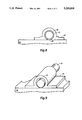
- FIG. 9 shows an perspective view of a cylinder that slides in a casing as a result of the process steps shown in FIGS. 1-9;
- micromechanical elements are built upon a substrate.
- silicon is used for the substrate.
- Silicon is ideal since it is not damaged during high temperature process steps.
- This is a process for a self-constraining joint is a rod or cylindrical structure that may slide and/or rotate within a casing.
- FIG. 1 illustrates the substrate 40 after depositing the first structural layer 42.
- the first structural layer 42 comprises of three layers, a first nitride layer 44, a doped polysilicon layer 46, and a second nitride layer 48.
- the first structural layer 42 undergoes two phases of patterning.
- the first step is done using conventional photoresist and etching processes and the results are shown in FIG. 2.
- the remaining first structural layer 42 will define where the self-constrained structure will be on the substrate 40.
- the second patterning phase is oxidation.
- An oxide bumper 50 is grown on the doped polysilicon layer 46 using a conventional oxidation process. The oxide grows on the exposed edge or wall of the doped polysilicon layer 46. The oxide bumper 50 grows both inward and outward in a curved shape since the constraints put on it from the first and second nitride layers 44 and 48 control the shape of the bumper. The oxidation rate will be slowest at the interface of the doped polysilicon layer 46 with each of the nitride layers 44 and 48. The oxide bumper 50 is grown until the profile of the oxide growth is circular.
- Oxidation rates can be controlled by changing the dopant profile of the doped polysilicon layer 46 either by ion implantation or by controlling in situ dopant in the doped polysilicon layer 46. Since control of polysilicon oxidation rates is known, the depth and profile of the oxide bumper 50 can be precisely controlled. The growth and control of oxide bumpers is discussed in U.S. Pat. Nos. 4,400,866 and 4,375,643 by Bol and Keming, both titled Application of Grown Oxide Bumper Insulators to a High Speed VLSI SASMEFET, incorporated by reference herein. Since the control of polysilicon oxidation rates is known, the size and shape of the oxide bumper can be precisely controlled.
- the oxide bumper is grown as shown in FIG. 3. In this sequence, attainment of a near circular oxide bumper is important.
- the oxide bumper 50 As shown in FIG. 4, most of the first structural layer 42 is removed and the oxide bumper 50 remains separated from the substrate by a small portion of nitride layer 44 which also remains. The oxide bumper 50 will become a rod that can move inside a casing.
- the next step is covering the oxide bumper 50 with a sacrificial nitride layer 52 as shown in FIG. 5.
- a nitride layer is deposited by conventional means.
- the nitride is then patterned using the same photoresist and etching technique used to pattern the first structural layer 42 in FIG. 28.
- the excess nitride is removed and the result is shown in FIG. 6.
- the entire oxide bumper 50 is covered with a nitride layer 52 and separated from the substrate 40 by nitride.
- the structure is now ready for deposition of the second structural layer 54, as shown in FIG. 7.
- Polysilicon has been used in this embodiment although other materials are also appropriate.
- the second structural layer 54 is separated from the oxide bumper 50 by the sacrificial layer 52.
- FIG. 8 shows the device after patterning the second structural layer 54.
- a rod 56 that can slide or rotate in a casing 58 has been finished except for the etching away of the sacrificial layer 52.
- the final step is a nitride etch to wash out the sacrificial layer 52. This step frees the rod 56 from its casing 58 and the substrate 40.
Abstract
Description
Claims (5)
Priority Applications (5)
| Application Number | Priority Date | Filing Date | Title |
|---|---|---|---|
| US07/725,173 US5209818A (en) | 1991-07-03 | 1991-07-03 | Manufacture of a micromechanical element with two degrees of freedom |
| CA002063508A CA2063508C (en) | 1991-07-03 | 1992-03-19 | Manufacture of a micromechanical element with two degrees of freedom |
| JP16950392A JP3269662B2 (en) | 1991-07-03 | 1992-06-26 | Manufacturing of micro-engineered elements |
| DE69219520T DE69219520T2 (en) | 1991-07-03 | 1992-07-01 | Production of a micromechanical element with two degrees of freedom |
| EP92306092A EP0521713B1 (en) | 1991-07-03 | 1992-07-01 | Manufacture of a micromechanical element with two degrees of freedom |
Applications Claiming Priority (1)
| Application Number | Priority Date | Filing Date | Title |
|---|---|---|---|
| US07/725,173 US5209818A (en) | 1991-07-03 | 1991-07-03 | Manufacture of a micromechanical element with two degrees of freedom |
Publications (1)
| Publication Number | Publication Date |
|---|---|
| US5209818A true US5209818A (en) | 1993-05-11 |
Family
ID=24913451
Family Applications (1)
| Application Number | Title | Priority Date | Filing Date |
|---|---|---|---|
| US07/725,173 Expired - Lifetime US5209818A (en) | 1991-07-03 | 1991-07-03 | Manufacture of a micromechanical element with two degrees of freedom |
Country Status (5)
| Country | Link |
|---|---|
| US (1) | US5209818A (en) |
| EP (1) | EP0521713B1 (en) |
| JP (1) | JP3269662B2 (en) |
| CA (1) | CA2063508C (en) |
| DE (1) | DE69219520T2 (en) |
Cited By (3)
| Publication number | Priority date | Publication date | Assignee | Title |
|---|---|---|---|---|
| US5659195A (en) * | 1995-06-08 | 1997-08-19 | The Regents Of The University Of California | CMOS integrated microsensor with a precision measurement circuit |
| US6093330A (en) * | 1997-06-02 | 2000-07-25 | Cornell Research Foundation, Inc. | Microfabrication process for enclosed microstructures |
| US6180536B1 (en) | 1998-06-04 | 2001-01-30 | Cornell Research Foundation, Inc. | Suspended moving channels and channel actuators for microfluidic applications and method for making |
Families Citing this family (5)
| Publication number | Priority date | Publication date | Assignee | Title |
|---|---|---|---|---|
| IL123579A0 (en) | 1998-03-06 | 1998-10-30 | Heines Amihai | Apparatus for producing high contrast imagery |
| IL137206A0 (en) | 1999-10-31 | 2001-07-24 | Nanomotion Ltd | Piezoelectric motors and motor driving configurations |
| JP4611592B2 (en) * | 1999-12-06 | 2011-01-12 | 孝 西 | How to create a gear |
| AU2002224007A1 (en) * | 2000-11-22 | 2002-06-03 | Flixel Ltd. | Microelectromechanical display devices |
| CN108317233B (en) * | 2018-04-09 | 2023-06-20 | 中国工程物理研究院电子工程研究所 | Integrated assembling-free multilayer micro-gear structure applied to MEMS micro-nano processing |
Citations (3)
| Publication number | Priority date | Publication date | Assignee | Title |
|---|---|---|---|---|
| US4740410A (en) * | 1987-05-28 | 1988-04-26 | The Regents Of The University Of California | Micromechanical elements and methods for their fabrication |
| US4997521A (en) * | 1987-05-20 | 1991-03-05 | Massachusetts Institute Of Technology | Electrostatic micromotor |
| US5043043A (en) * | 1990-06-22 | 1991-08-27 | Massachusetts Institute Of Technology | Method for fabricating side drive electrostatic micromotor |
Family Cites Families (2)
| Publication number | Priority date | Publication date | Assignee | Title |
|---|---|---|---|---|
| US4375643A (en) * | 1980-02-14 | 1983-03-01 | Xerox Corporation | Application of grown oxide bumper insulators to a high-speed VLSI SASMESFET |
| CA1308596C (en) * | 1986-01-13 | 1992-10-13 | Rohm And Haas Company | Microplastic structures and method of manufacture |
-
1991
- 1991-07-03 US US07/725,173 patent/US5209818A/en not_active Expired - Lifetime
-
1992
- 1992-03-19 CA CA002063508A patent/CA2063508C/en not_active Expired - Lifetime
- 1992-06-26 JP JP16950392A patent/JP3269662B2/en not_active Expired - Lifetime
- 1992-07-01 EP EP92306092A patent/EP0521713B1/en not_active Expired - Lifetime
- 1992-07-01 DE DE69219520T patent/DE69219520T2/en not_active Expired - Lifetime
Patent Citations (3)
| Publication number | Priority date | Publication date | Assignee | Title |
|---|---|---|---|---|
| US4997521A (en) * | 1987-05-20 | 1991-03-05 | Massachusetts Institute Of Technology | Electrostatic micromotor |
| US4740410A (en) * | 1987-05-28 | 1988-04-26 | The Regents Of The University Of California | Micromechanical elements and methods for their fabrication |
| US5043043A (en) * | 1990-06-22 | 1991-08-27 | Massachusetts Institute Of Technology | Method for fabricating side drive electrostatic micromotor |
Cited By (4)
| Publication number | Priority date | Publication date | Assignee | Title |
|---|---|---|---|---|
| US5659195A (en) * | 1995-06-08 | 1997-08-19 | The Regents Of The University Of California | CMOS integrated microsensor with a precision measurement circuit |
| US6093330A (en) * | 1997-06-02 | 2000-07-25 | Cornell Research Foundation, Inc. | Microfabrication process for enclosed microstructures |
| US6180536B1 (en) | 1998-06-04 | 2001-01-30 | Cornell Research Foundation, Inc. | Suspended moving channels and channel actuators for microfluidic applications and method for making |
| US6462391B1 (en) | 1998-06-04 | 2002-10-08 | Cornell Research Foundation, Inc. | Suspended moving channels and channel actuators for microfluidic applications and method for making |
Also Published As
| Publication number | Publication date |
|---|---|
| EP0521713B1 (en) | 1997-05-07 |
| DE69219520D1 (en) | 1997-06-12 |
| DE69219520T2 (en) | 1997-11-06 |
| JPH05230680A (en) | 1993-09-07 |
| CA2063508A1 (en) | 1993-01-04 |
| JP3269662B2 (en) | 2002-03-25 |
| EP0521713A1 (en) | 1993-01-07 |
| CA2063508C (en) | 1999-07-13 |
Similar Documents
| Publication | Publication Date | Title |
|---|---|---|
| EP0683921B1 (en) | Microstructures and single mask, single-crystal process for fabrication thereof | |
| US7507669B2 (en) | Gap tuning for surface micromachined structures in an epitaxial reactor | |
| US5209818A (en) | Manufacture of a micromechanical element with two degrees of freedom | |
| EP0981168A3 (en) | Semiconductor micro-optical components and method for producing them | |
| JPH10506717A (en) | Manufacturing method of acceleration sensor | |
| JP2023002750A (en) | Mems grid for operating structure parameter of mems device | |
| US5149397A (en) | Fabrication methods for micromechanical elements | |
| US5151153A (en) | Manufacture of a suspended micromechanical element | |
| US5417801A (en) | Process to manufacture bushings for micromechanical elements | |
| US6544863B1 (en) | Method of fabricating semiconductor wafers having multiple height subsurface layers | |
| US5256248A (en) | Method for patterning semiconductor | |
| JP3464500B2 (en) | Chip forming process | |
| WO2001011666A9 (en) | Method of etching a wafer layer using multiple layers of the same photoresistant material and structure formed thereby | |
| JPS63119239A (en) | Manufacture of semiconductor device | |
| US6429034B1 (en) | Method of making high aspect ratio features during surface micromachining | |
| JPS6289324A (en) | Manufacture of semiconductor device | |
| JPH03294396A (en) | Micromechanics and production thereof | |
| JPS6083331A (en) | Forming method of groove | |
| JPS6312381B2 (en) | ||
| JPH03201460A (en) | Manufacture of dielectric isolation substrate | |
| JPH10232241A (en) | Manufacture of cantilever | |
| JPS61285726A (en) | Formation of fine pattern | |
| JPH01183119A (en) | Preparation of x-ray mask | |
| JPS6112030A (en) | Pattern forming method using two-layer resist | |
| JPH02205014A (en) | Manufacture of semiconductor device |
Legal Events
| Date | Code | Title | Description |
|---|---|---|---|
| AS | Assignment |
Owner name: XEROX CORPORATION Free format text: ASSIGNMENT OF ASSIGNORS INTEREST.;ASSIGNOR:BOL, IGOR I.;REEL/FRAME:005776/0046 Effective date: 19910703 |
|
| STCF | Information on status: patent grant |
Free format text: PATENTED CASE |
|
| FEPP | Fee payment procedure |
Free format text: PAYOR NUMBER ASSIGNED (ORIGINAL EVENT CODE: ASPN); ENTITY STATUS OF PATENT OWNER: LARGE ENTITY |
|
| FPAY | Fee payment |
Year of fee payment: 4 |
|
| FPAY | Fee payment |
Year of fee payment: 8 |
|
| AS | Assignment |
Owner name: BANK ONE, NA, AS ADMINISTRATIVE AGENT, ILLINOIS Free format text: SECURITY INTEREST;ASSIGNOR:XEROX CORPORATION;REEL/FRAME:013153/0001 Effective date: 20020621 |
|
| AS | Assignment |
Owner name: JPMORGAN CHASE BANK, AS COLLATERAL AGENT, TEXAS Free format text: SECURITY AGREEMENT;ASSIGNOR:XEROX CORPORATION;REEL/FRAME:015134/0476 Effective date: 20030625 Owner name: JPMORGAN CHASE BANK, AS COLLATERAL AGENT,TEXAS Free format text: SECURITY AGREEMENT;ASSIGNOR:XEROX CORPORATION;REEL/FRAME:015134/0476 Effective date: 20030625 |
|
| FPAY | Fee payment |
Year of fee payment: 12 |
|
| AS | Assignment |
Owner name: XEROX CORPORATION, CONNECTICUT Free format text: RELEASE BY SECURED PARTY;ASSIGNOR:JPMORGAN CHASE BANK, N.A. AS SUCCESSOR-IN-INTEREST ADMINISTRATIVE AGENT AND COLLATERAL AGENT TO JPMORGAN CHASE BANK;REEL/FRAME:066728/0193 Effective date: 20220822 |