US5216588A - Charge pump with high output current - Google Patents
Charge pump with high output current Download PDFInfo
- Publication number
- US5216588A US5216588A US07/837,172 US83717292A US5216588A US 5216588 A US5216588 A US 5216588A US 83717292 A US83717292 A US 83717292A US 5216588 A US5216588 A US 5216588A
- Authority
- US
- United States
- Prior art keywords
- circuit
- signal
- charge pump
- voltage
- pump
- Prior art date
- Legal status (The legal status is an assumption and is not a legal conclusion. Google has not performed a legal analysis and makes no representation as to the accuracy of the status listed.)
- Expired - Lifetime
Links
Images


Classifications
-
- H—ELECTRICITY
- H02—GENERATION; CONVERSION OR DISTRIBUTION OF ELECTRIC POWER
- H02M—APPARATUS FOR CONVERSION BETWEEN AC AND AC, BETWEEN AC AND DC, OR BETWEEN DC AND DC, AND FOR USE WITH MAINS OR SIMILAR POWER SUPPLY SYSTEMS; CONVERSION OF DC OR AC INPUT POWER INTO SURGE OUTPUT POWER; CONTROL OR REGULATION THEREOF
- H02M3/00—Conversion of dc power input into dc power output
- H02M3/02—Conversion of dc power input into dc power output without intermediate conversion into ac
- H02M3/04—Conversion of dc power input into dc power output without intermediate conversion into ac by static converters
- H02M3/06—Conversion of dc power input into dc power output without intermediate conversion into ac by static converters using resistors or capacitors, e.g. potential divider
- H02M3/07—Conversion of dc power input into dc power output without intermediate conversion into ac by static converters using resistors or capacitors, e.g. potential divider using capacitors charged and discharged alternately by semiconductor devices with control electrode, e.g. charge pumps
Definitions
- This invention relates to power converters and more particularly to charge pump circuits.
- Power converter circuits that convert a low voltage to a higher voltage are frequently required within electrical systems.
- One type of power converter circuit known as a charge pump typically includes a diode-capacitor voltage multiplier to achieve the voltage conversion.
- charge pump circuits have typically been limited to applications that require relatively low current.
- a charge pump circuit that enables the conversion of a low voltage to a higher voltage while delivering a substantial amount of current.
- the charge pump circuit includes a plurality of diode-capacitor voltage multiplier pump units connected in parallel with respect to each other. The plurality of pump units are switched at different times during the pump frequency to minimize noise generation.
- the charge pump circuit is capable of delivering 8 mA of current.
- a charge pump circuit comprises a first voltage pump unit including at least a first capacitor coupled to a voltage output line that is charged in response to a first clocking signal, and a second voltage pump unit including at least a second capacitor coupled to the voltage output line that is charged in response to a second clocking signal having an unequal phase relative to the first clocking signal.
- a charge pump circuit comprises a ring oscillator circuit for providing a plurality of clocking signals, each having an unequal phase with respect to the other.
- the charge pump circuit further comprises a plurality of clock control units, each coupled to receive a separate clocking signal from the ring oscillator circuit.
- a plurality of voltage pump units are each coupled to a separate clock control unit.
- FIG. 1 is a block diagram illustrating a charge pump circuit in accordance with the present invention.
- FIG. 2 is a schematic diagram illustrating an oscillator circuit with stepped clock signals.
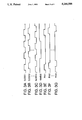
- FIGS. 3A-3G are timing diagrams illustrating the stepped clock signals and the clock control unit output signals.
- FIG. 4 is a schematic diagram illustrating a clock control unit and a pump unit incorporated within the charge pump circuit.
- FIG. 1 a block diagram is shown that illustrates a charge pump circuit in accordance with the present invention.
- the charge pump circuit includes a ring oscillator circuit 200, eight clock control units 250-A through 250-H, and eight voltage multiplier pump units 300-A through 300-H.
- the ring oscillator circuit 200 generates eight clock signals CLOCK1-CLOCK8 each having an equal frequency and an unequal phase. As shown, a separate clock signal is provided to each of the clock control units 250-A through 250-H.
- the clock control units 250-A through 250-H generate signals PHI1-PHI8 that drive the pump units 300-A through 300-H respectively.
- the pump units 300-A through 300-H are connected in parallel and are implemented using diode-capacitor voltage multipliers to thereby generate a high voltage at output line 306.
- the ring oscillator 200 and clock control units 250A-250H are configured such that the pump units 300-A through 300-H are always switched at different times with respect to one another. Thus, large voltage spikes do not result. This operation will be better understood with reference to the schematic and timing diagrams of FIGS. 2-4.
- FIG. 2 is a schematic diagram that illustrates the ring oscillator circuit 200.
- the ring oscillator circuit includes nine P-channel field effect transistors 202-A through 202-I, nine N-channel field effect transistors 204-A through 204-I, and nine inverters 206-A through 206-I.
- the circuit further includes a bias and control unit 210.
- FIGS. 3A-3C are timing diagram illustrating the clock signals CLOCK1, CLOCK2 and CLOCK8 generated by ring oscillator circuit 200. It is noted that the bias and control unit 210 is designed such that the generated clock signals CLOCK1-CLOCK8 have a desired pump frequency and that each of the clock signals CLOCK1-CLOCK8 are delayed with respect to one another due to inverters 206-A through 206-I. As mentioned previously and as shown in FIG. 1, a separate clock signal CLOCK1-CLOCK8 is provided to each of clock control units 250-A through 250-H.
- FIG. 4 a schematic diagram is shown that includes a clock control unit 250 and a pump unit 300. It is noted that clock control unit 250 is representative of each of the clock control units 250-A through 250-H of FIG. 1 and that pump unit 300 is representative of each of the pump units 300-A through 300-H of FIG. 1.
- the clock control unit 250 includes NAND gates 252-256, inverters 260-269, P-channel field effect transistors 271 and 272, and N-channel field effect transistors 274 and 275.
- the clock control unit 250 is enabled by an enable signal at line 280, and receives one of the clock signals CLOCK1-CLOCK8 at line 285.
- the clock control unit 250 is disabled when the enable signal at line 280 is low and is enabled when the enable signal is high. As illustrated in FIGS. 3D-3G, the output signal PHI (i.e., one of signals PHI1-PHI8) of the corresponding clock control unit 250 follows the state of the associated clock signal CLOCK1-CLOCK8 when the ENABLE signal is high. When the ENABLE signal goes low, the state of the signal PHI cannot change. When the ENABLE signal returns high, the state of the signal PHI does not change states until a corresponding change occurs in the associated clock signal.
- the output signal PHI i.e., one of signals PHI1-PHI8
- a latch circuit consisting of inverters 264 and 265 is used to store the state of the clock signal when the ENABLE signal goes low.
- transistors 272 and 274 are both turned off.
- a flip-flop circuit consisting of NAND gates 253 and 254 is used to release the latch circuit (inverters 264, 265) when the clock signal goes low following reassertion of the ENABLE signal.
- the falling edge of the clock signal is detected by inverters 260 and 261 and NAND gate 252.
- Inverters 266-269 and a flip-flop circuitry consisting of NAND gates 255 and 256 prevent overlap in the PHI and PHI signals.
- the pump unit 300 includes a plurality of N-channel field effect transistors 301, 302A-302F and 304A-304F. It is noted that transistors 302A-302F are connected as capacitors and that transistors 304A-304F are connected as diodes. The circuit thus forms a diode-capacitor voltage multiplier.
- signals PHI and PHI generated by the corresponding clock control unit 250 alternately charge the capacitances established by transistors 302A-302F.
- the discharge of the voltage across the capacitances is prevented since current cannot flow in a reverse direction through the diodes established by transistors 304A-304F. Accordingly, the voltage at output line 306 increases as the capacitances of transistors 302A-302F are charged.
- the pump unit 300 utilizes field effect transistors to implement the diode-capacitor voltage multipliers since the circuit is incorporated on an integrated circuit.
- the pump unit 300 could alternatively be implemented using actual capacitors and diodes.
- the number of diode-capacitor stages controls the overall voltage level charged at output line 306. The number of diode-capacitor stages utilized could be varied without departing from the scope of the invention.
- the pump units 300-A through 300-H are each switched on and off at different times. Consequently, minimal noise is generated at output line 306 in relation to the current capacity.
- circuit of FIG. 1 includes eight pump units 300-A through 300-H, the invention is equally applicable to circuits having a greater or lesser number of pump units connected in parallel.
- the number of pump units chosen for a particular application will depend upon the current requirements and the component values.
Abstract
Description
Claims (6)
Priority Applications (1)
| Application Number | Priority Date | Filing Date | Title |
|---|---|---|---|
| US07/837,172 US5216588A (en) | 1992-02-14 | 1992-02-14 | Charge pump with high output current |
Applications Claiming Priority (1)
| Application Number | Priority Date | Filing Date | Title |
|---|---|---|---|
| US07/837,172 US5216588A (en) | 1992-02-14 | 1992-02-14 | Charge pump with high output current |
Publications (1)
| Publication Number | Publication Date |
|---|---|
| US5216588A true US5216588A (en) | 1993-06-01 |
Family
ID=25273719
Family Applications (1)
| Application Number | Title | Priority Date | Filing Date |
|---|---|---|---|
| US07/837,172 Expired - Lifetime US5216588A (en) | 1992-02-14 | 1992-02-14 | Charge pump with high output current |
Country Status (1)
| Country | Link |
|---|---|
| US (1) | US5216588A (en) |
Cited By (46)
| Publication number | Priority date | Publication date | Assignee | Title |
|---|---|---|---|---|
| US5280420A (en) * | 1992-10-02 | 1994-01-18 | National Semiconductor Corporation | Charge pump which operates on a low voltage power supply |
| US5301097A (en) * | 1992-06-10 | 1994-04-05 | Intel Corporation | Multi-staged charge-pump with staggered clock phases for providing high current capability |
| US5313429A (en) * | 1992-02-14 | 1994-05-17 | Catalyst Semiconductor, Inc. | Memory circuit with pumped voltage for erase and program operations |
| US5363335A (en) * | 1993-09-28 | 1994-11-08 | Intel Corporation | Nonvolatile memory with automatic power supply configuration |
| EP0646924A1 (en) * | 1993-09-30 | 1995-04-05 | STMicroelectronics S.r.l. | Voltage booster circuit for generating both positive and negative boosted voltages |
| DE4335857A1 (en) * | 1993-10-21 | 1995-04-27 | Abb Management Ag | Converter circuit arrangement and method for driving the same |
| US5426391A (en) * | 1993-09-10 | 1995-06-20 | Intel Corporation | Method and apparatus for providing selectable sources of voltage |
| US5432469A (en) * | 1993-09-10 | 1995-07-11 | Intel Corporation | Method and apparatus for a two phase bootstrap charge pump |
| US5442586A (en) * | 1993-09-10 | 1995-08-15 | Intel Corporation | Method and apparatus for controlling the output current provided by a charge pump circuit |
| US5483486A (en) * | 1994-10-19 | 1996-01-09 | Intel Corporation | Charge pump circuit for providing multiple output voltages for flash memory |
| US5532915A (en) * | 1994-03-23 | 1996-07-02 | Intel Corporation | Method and apparatus for providing an ultra low power regulated negative charge pump |
| US5553030A (en) * | 1993-09-10 | 1996-09-03 | Intel Corporation | Method and apparatus for controlling the output voltage provided by a charge pump circuit |
| US5553295A (en) * | 1994-03-23 | 1996-09-03 | Intel Corporation | Method and apparatus for regulating the output voltage of negative charge pumps |
| EP0738436A1 (en) * | 1993-12-08 | 1996-10-23 | International Power Systems,Inc. | Phased array power processor and method of operating same |
| US5583384A (en) * | 1995-06-07 | 1996-12-10 | National Semiconductor Corporation | Method and apparatus for connecting and disconnecting a power field effect transistor |
| US5614814A (en) * | 1993-12-28 | 1997-03-25 | Sanyo Electric Co., Ltd. | Negative voltage genarating circuit |
| US5625544A (en) * | 1996-04-25 | 1997-04-29 | Programmable Microelectronics Corp. | Charge pump |
| US5663918A (en) * | 1994-10-19 | 1997-09-02 | Intel Corporation | Method and apparatus for detecting and selecting voltage supplies for flash memory |
| US5692164A (en) * | 1994-03-23 | 1997-11-25 | Intel Corporation | Method and apparatus for generating four phase non-over lapping clock pulses for a charge pump |
| US5781477A (en) * | 1996-02-23 | 1998-07-14 | Micron Quantum Devices, Inc. | Flash memory system having fast erase operation |
| US5841703A (en) * | 1996-12-31 | 1998-11-24 | Intel Corporation | Method and apparatus for removal of VT drop in the output diode of charge pumps |
| US5841165A (en) * | 1995-11-21 | 1998-11-24 | Programmable Microelectronics Corporation | PMOS flash EEPROM cell with single poly |
| US5892670A (en) * | 1996-12-12 | 1999-04-06 | Cypress Semiconductor Corporation | Charge pump architecture |
| US5907484A (en) * | 1996-04-25 | 1999-05-25 | Programmable Microelectronics Corp. | Charge pump |
| US5923509A (en) * | 1994-09-20 | 1999-07-13 | Matsushita Electric Industrial Co., Ltd. | Disk cartridge with judging recesses |
| US5959854A (en) * | 1997-06-30 | 1999-09-28 | Nec Corporation | Voltage step-up circuit and method for controlling the same |
| US5999425A (en) * | 1998-01-15 | 1999-12-07 | Cypress Semiconductor Corp. | Charge pump architecture for integrated circuit |
| US6018479A (en) * | 1998-08-10 | 2000-01-25 | Lg Semicon Co., Ltd. | High voltage generating circuit for a semiconductor memory device |
| US6163494A (en) * | 1999-01-29 | 2000-12-19 | Linear Technology Corporation | IC with enhanced low voltage start-up |
| US6163205A (en) * | 1997-11-04 | 2000-12-19 | Robert Bosch Gmbh | Charge pump |
| US6243299B1 (en) | 1998-02-27 | 2001-06-05 | Micron Technology, Inc. | Flash memory system having fast erase operation |
| US6486728B2 (en) | 2001-03-16 | 2002-11-26 | Matrix Semiconductor, Inc. | Multi-stage charge pump |
| US6605984B2 (en) * | 2002-01-02 | 2003-08-12 | Intel Corporation | Charge pump ripple reduction |
| US6650172B1 (en) * | 1999-07-08 | 2003-11-18 | Nec Electronics Corporation | Boost circuit with sequentially delayed activation of pump circuit stages |
| US20040046603A1 (en) * | 2002-09-06 | 2004-03-11 | Lorenzo Bedarida | Modular charge pump architecture |
| US20090097285A1 (en) * | 2007-10-10 | 2009-04-16 | Cook Thomas D | Variable load, variable output charge-based voltage multipliers |
| US20110156819A1 (en) * | 2008-07-18 | 2011-06-30 | Tae Youn Kim | Low-Noise High Efficiency Bias Generation Circuits and Method |
| US8013666B1 (en) * | 2009-07-31 | 2011-09-06 | Altera Corporation | Low ripple charge pump |
| US20120286854A1 (en) * | 2011-05-11 | 2012-11-15 | Swonger James W | High Voltage Ring Pump |
| US8816659B2 (en) | 2010-08-06 | 2014-08-26 | Peregrine Semiconductor Corporation | Low-noise high efficiency bias generation circuits and method |
| US9190902B2 (en) | 2003-09-08 | 2015-11-17 | Peregrine Semiconductor Corporation | Low noise charge pump method and apparatus |
| US9264053B2 (en) | 2011-01-18 | 2016-02-16 | Peregrine Semiconductor Corporation | Variable frequency charge pump |
| US9356506B1 (en) | 2015-04-01 | 2016-05-31 | Ememory Technology Inc. | Charge pump regulator and control method thereof |
| US9660590B2 (en) | 2008-07-18 | 2017-05-23 | Peregrine Semiconductor Corporation | Low-noise high efficiency bias generation circuits and method |
| US20180234095A1 (en) * | 2017-02-13 | 2018-08-16 | Skyworks Solutions, Inc. | Control circuitry for silicon-on-insulator chip |
| USRE47017E1 (en) | 2009-06-26 | 2018-08-28 | Toshiba Memory Corporation | Semiconductor device for short-circuiting output terminals of two or more voltage generator circuits at read time and control method for the same |
Citations (5)
| Publication number | Priority date | Publication date | Assignee | Title |
|---|---|---|---|---|
| US4199805A (en) * | 1977-11-21 | 1980-04-22 | Hughes Aircraft Company | Multiphase capacitor diode voltage multiplier |
| US4302804A (en) * | 1979-09-04 | 1981-11-24 | Burroughs Corporation | DC Voltage multiplier using phase-sequenced CMOS switches |
| US4933827A (en) * | 1988-07-06 | 1990-06-12 | Sgs-Thompson Microelectronics S.R.L. | Regulation of the output voltage of a voltage multiplier |
| US4962512A (en) * | 1987-06-26 | 1990-10-09 | Sharp Kabushiki Kaisha | Step-up circuit |
| US5008799A (en) * | 1990-04-05 | 1991-04-16 | Montalvo Antonio J | Back-to-back capacitor charge pumps |
-
1992
- 1992-02-14 US US07/837,172 patent/US5216588A/en not_active Expired - Lifetime
Patent Citations (5)
| Publication number | Priority date | Publication date | Assignee | Title |
|---|---|---|---|---|
| US4199805A (en) * | 1977-11-21 | 1980-04-22 | Hughes Aircraft Company | Multiphase capacitor diode voltage multiplier |
| US4302804A (en) * | 1979-09-04 | 1981-11-24 | Burroughs Corporation | DC Voltage multiplier using phase-sequenced CMOS switches |
| US4962512A (en) * | 1987-06-26 | 1990-10-09 | Sharp Kabushiki Kaisha | Step-up circuit |
| US4933827A (en) * | 1988-07-06 | 1990-06-12 | Sgs-Thompson Microelectronics S.R.L. | Regulation of the output voltage of a voltage multiplier |
| US5008799A (en) * | 1990-04-05 | 1991-04-16 | Montalvo Antonio J | Back-to-back capacitor charge pumps |
Cited By (70)
| Publication number | Priority date | Publication date | Assignee | Title |
|---|---|---|---|---|
| US5313429A (en) * | 1992-02-14 | 1994-05-17 | Catalyst Semiconductor, Inc. | Memory circuit with pumped voltage for erase and program operations |
| US5301097A (en) * | 1992-06-10 | 1994-04-05 | Intel Corporation | Multi-staged charge-pump with staggered clock phases for providing high current capability |
| US5280420A (en) * | 1992-10-02 | 1994-01-18 | National Semiconductor Corporation | Charge pump which operates on a low voltage power supply |
| US5553030A (en) * | 1993-09-10 | 1996-09-03 | Intel Corporation | Method and apparatus for controlling the output voltage provided by a charge pump circuit |
| US5446408A (en) * | 1993-09-10 | 1995-08-29 | Intel Corporation | Method and apparatus for providing selectable sources of voltage |
| US5524266A (en) * | 1993-09-10 | 1996-06-04 | Intel Corporation | System having multiple phase boosted charge pump with a plurality of stages |
| US5426391A (en) * | 1993-09-10 | 1995-06-20 | Intel Corporation | Method and apparatus for providing selectable sources of voltage |
| US5430402A (en) * | 1993-09-10 | 1995-07-04 | Intel Corporation | Method and apparatus for providing selectable sources of voltage |
| US5432469A (en) * | 1993-09-10 | 1995-07-11 | Intel Corporation | Method and apparatus for a two phase bootstrap charge pump |
| US5455794A (en) * | 1993-09-10 | 1995-10-03 | Intel Corporation | Method and apparatus for controlling the output current provided by a charge pump circuit |
| US5442586A (en) * | 1993-09-10 | 1995-08-15 | Intel Corporation | Method and apparatus for controlling the output current provided by a charge pump circuit |
| US5363335A (en) * | 1993-09-28 | 1994-11-08 | Intel Corporation | Nonvolatile memory with automatic power supply configuration |
| EP0646924A1 (en) * | 1993-09-30 | 1995-04-05 | STMicroelectronics S.r.l. | Voltage booster circuit for generating both positive and negative boosted voltages |
| US5546044A (en) * | 1993-09-30 | 1996-08-13 | Sgs-Thomson Microelectronics S.R.L. | Voltage generator circuit providing potentials of opposite polarity |
| US5566063A (en) * | 1993-10-21 | 1996-10-15 | Abb Management Ag | Electronic power converter circuit arrangement and method for driving same |
| DE4335857A1 (en) * | 1993-10-21 | 1995-04-27 | Abb Management Ag | Converter circuit arrangement and method for driving the same |
| EP0738436A1 (en) * | 1993-12-08 | 1996-10-23 | International Power Systems,Inc. | Phased array power processor and method of operating same |
| EP0738436A4 (en) * | 1993-12-08 | 1997-05-07 | Int Power Systems Inc | Phased array power processor and method of operating same |
| US5614814A (en) * | 1993-12-28 | 1997-03-25 | Sanyo Electric Co., Ltd. | Negative voltage genarating circuit |
| US5692164A (en) * | 1994-03-23 | 1997-11-25 | Intel Corporation | Method and apparatus for generating four phase non-over lapping clock pulses for a charge pump |
| US5553295A (en) * | 1994-03-23 | 1996-09-03 | Intel Corporation | Method and apparatus for regulating the output voltage of negative charge pumps |
| US5532915A (en) * | 1994-03-23 | 1996-07-02 | Intel Corporation | Method and apparatus for providing an ultra low power regulated negative charge pump |
| US5923509A (en) * | 1994-09-20 | 1999-07-13 | Matsushita Electric Industrial Co., Ltd. | Disk cartridge with judging recesses |
| US5663918A (en) * | 1994-10-19 | 1997-09-02 | Intel Corporation | Method and apparatus for detecting and selecting voltage supplies for flash memory |
| US5483486A (en) * | 1994-10-19 | 1996-01-09 | Intel Corporation | Charge pump circuit for providing multiple output voltages for flash memory |
| US5583384A (en) * | 1995-06-07 | 1996-12-10 | National Semiconductor Corporation | Method and apparatus for connecting and disconnecting a power field effect transistor |
| US5841165A (en) * | 1995-11-21 | 1998-11-24 | Programmable Microelectronics Corporation | PMOS flash EEPROM cell with single poly |
| US5917755A (en) * | 1996-02-23 | 1999-06-29 | Micron Technology, Inc. | Flash memory system having fast erase operation |
| US5781477A (en) * | 1996-02-23 | 1998-07-14 | Micron Quantum Devices, Inc. | Flash memory system having fast erase operation |
| US5625544A (en) * | 1996-04-25 | 1997-04-29 | Programmable Microelectronics Corp. | Charge pump |
| US5907484A (en) * | 1996-04-25 | 1999-05-25 | Programmable Microelectronics Corp. | Charge pump |
| US5892670A (en) * | 1996-12-12 | 1999-04-06 | Cypress Semiconductor Corporation | Charge pump architecture |
| US5841703A (en) * | 1996-12-31 | 1998-11-24 | Intel Corporation | Method and apparatus for removal of VT drop in the output diode of charge pumps |
| US5959854A (en) * | 1997-06-30 | 1999-09-28 | Nec Corporation | Voltage step-up circuit and method for controlling the same |
| US6163205A (en) * | 1997-11-04 | 2000-12-19 | Robert Bosch Gmbh | Charge pump |
| US5999425A (en) * | 1998-01-15 | 1999-12-07 | Cypress Semiconductor Corp. | Charge pump architecture for integrated circuit |
| US6243299B1 (en) | 1998-02-27 | 2001-06-05 | Micron Technology, Inc. | Flash memory system having fast erase operation |
| US6018479A (en) * | 1998-08-10 | 2000-01-25 | Lg Semicon Co., Ltd. | High voltage generating circuit for a semiconductor memory device |
| DE19936853B4 (en) * | 1998-08-10 | 2011-12-01 | Lg Semicon Co., Ltd. | High voltage generator circuit for a semiconductor memory |
| US6163494A (en) * | 1999-01-29 | 2000-12-19 | Linear Technology Corporation | IC with enhanced low voltage start-up |
| US6650172B1 (en) * | 1999-07-08 | 2003-11-18 | Nec Electronics Corporation | Boost circuit with sequentially delayed activation of pump circuit stages |
| US6486728B2 (en) | 2001-03-16 | 2002-11-26 | Matrix Semiconductor, Inc. | Multi-stage charge pump |
| US6605984B2 (en) * | 2002-01-02 | 2003-08-12 | Intel Corporation | Charge pump ripple reduction |
| US20040046603A1 (en) * | 2002-09-06 | 2004-03-11 | Lorenzo Bedarida | Modular charge pump architecture |
| US6794927B2 (en) | 2002-09-06 | 2004-09-21 | Atmel Corporation | Modular charge pump architecture |
| WO2004023231A1 (en) * | 2002-09-06 | 2004-03-18 | Atmel Corporation | Modular charge pump architecture |
| US10965276B2 (en) | 2003-09-08 | 2021-03-30 | Psemi Corporation | Low noise charge pump method and apparatus |
| US9190902B2 (en) | 2003-09-08 | 2015-11-17 | Peregrine Semiconductor Corporation | Low noise charge pump method and apparatus |
| US20090097285A1 (en) * | 2007-10-10 | 2009-04-16 | Cook Thomas D | Variable load, variable output charge-based voltage multipliers |
| US7889523B2 (en) | 2007-10-10 | 2011-02-15 | Freescale Semiconductor, Inc. | Variable load, variable output charge-based voltage multipliers |
| US9660590B2 (en) | 2008-07-18 | 2017-05-23 | Peregrine Semiconductor Corporation | Low-noise high efficiency bias generation circuits and method |
| US20110156819A1 (en) * | 2008-07-18 | 2011-06-30 | Tae Youn Kim | Low-Noise High Efficiency Bias Generation Circuits and Method |
| US9429969B2 (en) | 2008-07-18 | 2016-08-30 | Peregrine Semiconductor Corporation | Low-noise high efficiency bias generation circuits and method |
| US8994452B2 (en) | 2008-07-18 | 2015-03-31 | Peregrine Semiconductor Corporation | Low-noise high efficiency bias generation circuits and method |
| USRE49175E1 (en) | 2009-06-26 | 2022-08-16 | Kioxia Corporation | Semiconductor device including three voltage generator circuits and two transistors configured to short-circuit respective different combinations of the voltage generator circuits |
| USRE47017E1 (en) | 2009-06-26 | 2018-08-28 | Toshiba Memory Corporation | Semiconductor device for short-circuiting output terminals of two or more voltage generator circuits at read time and control method for the same |
| US8013666B1 (en) * | 2009-07-31 | 2011-09-06 | Altera Corporation | Low ripple charge pump |
| US11662755B2 (en) | 2010-08-06 | 2023-05-30 | Psemi Corporation | Low-noise high efficiency bias generation circuits and method |
| US11188106B2 (en) | 2010-08-06 | 2021-11-30 | Psemi Corporation | Low-noise high efficiency bias generation circuits and method |
| US8816659B2 (en) | 2010-08-06 | 2014-08-26 | Peregrine Semiconductor Corporation | Low-noise high efficiency bias generation circuits and method |
| US9413362B2 (en) | 2011-01-18 | 2016-08-09 | Peregrine Semiconductor Corporation | Differential charge pump |
| US9264053B2 (en) | 2011-01-18 | 2016-02-16 | Peregrine Semiconductor Corporation | Variable frequency charge pump |
| US20120286854A1 (en) * | 2011-05-11 | 2012-11-15 | Swonger James W | High Voltage Ring Pump |
| US8686787B2 (en) * | 2011-05-11 | 2014-04-01 | Peregrine Semiconductor Corporation | High voltage ring pump with inverter stages and voltage boosting stages |
| US9354654B2 (en) | 2011-05-11 | 2016-05-31 | Peregrine Semiconductor Corporation | High voltage ring pump with inverter stages and voltage boosting stages |
| US9356506B1 (en) | 2015-04-01 | 2016-05-31 | Ememory Technology Inc. | Charge pump regulator and control method thereof |
| US20180234095A1 (en) * | 2017-02-13 | 2018-08-16 | Skyworks Solutions, Inc. | Control circuitry for silicon-on-insulator chip |
| US11190182B2 (en) * | 2017-02-13 | 2021-11-30 | Skyworks Solutions, Inc. | Control circuitry for silicon-on-insulator chip |
| US20220085808A1 (en) * | 2017-02-13 | 2022-03-17 | Skyworks Solutions, Inc. | Voltage generators with charge pumps for switch circuits |
| US11689202B2 (en) * | 2017-02-13 | 2023-06-27 | Skyworks Solutions, Inc. | Voltage generators with charge pumps for switch circuits |
Similar Documents
| Publication | Publication Date | Title |
|---|---|---|
| US5216588A (en) | Charge pump with high output current | |
| US4807104A (en) | Voltage multiplying and inverting charge pump | |
| US6154088A (en) | Clocking scheme and charge transfer switch for increasing the efficiency of a charge pump or other circuit | |
| CA2251378C (en) | High-speed and high-precision phase locked loop | |
| US6020781A (en) | Step-up circuit using two frequencies | |
| US5982222A (en) | High voltage generating circuit for a semiconductor memory device | |
| KR950002726B1 (en) | Charge-pump circuit of substrate voltage generator | |
| US6909319B2 (en) | Low power charge pump method and apparatus | |
| EP0598260A1 (en) | High frequency voltage controlled oscillator | |
| KR100300077B1 (en) | Charge pump circuit having adaptive oscillation period | |
| US5519360A (en) | Ring oscillator enable circuit with immediate shutdown | |
| US5760623A (en) | Ramp voltage generator for differential switching amplifiers | |
| US5463542A (en) | DC/DC converter and RS-232 interface circuit using the same | |
| US6229385B1 (en) | Control feature for IC without using a dedicated pin | |
| US5051882A (en) | Three reservoir capacitor charge pump circuit | |
| KR20050070110A (en) | Capacitive charge pump | |
| US20080054990A1 (en) | Charge pump method and architecture | |
| US4888677A (en) | Three reservoir capacitor | |
| US7724073B2 (en) | Charge pump circuit | |
| US6667662B2 (en) | Oscillator circuit of internal power generator circuit and control method thereof | |
| US5621360A (en) | Voltage supply isolation buffer | |
| US6067336A (en) | Charge pump circuit | |
| US6831500B2 (en) | Noise-reduced voltage boosting circuit | |
| US20040021504A1 (en) | Boosting circuit configured with plurality of boosting circuit units in series | |
| US5398001A (en) | Self-timing four-phase clock generator |
Legal Events
| Date | Code | Title | Description |
|---|---|---|---|
| AS | Assignment |
Owner name: CATALYST SEMICONDUTOR, INC., A CA CORP., CALIFORNI Free format text: ASSIGNMENT OF ASSIGNORS INTEREST.;ASSIGNORS:BAJWA, ASIM A.;CHEVALLIER, CHRISTOPHE J.;REEL/FRAME:006091/0946 Effective date: 19920214 |
|
| STCF | Information on status: patent grant |
Free format text: PATENTED CASE |
|
| FEPP | Fee payment procedure |
Free format text: PAT HLDR NO LONGER CLAIMS SMALL ENT STAT AS SMALL BUSINESS (ORIGINAL EVENT CODE: LSM2); ENTITY STATUS OF PATENT OWNER: SMALL ENTITY |
|
| AS | Assignment |
Owner name: COMERICA BANK - CALIFORNIA, CALIFORNIA Free format text: SECURITY INTEREST;ASSIGNOR:CATALYST SEMICONDUCTOR, INC.;REEL/FRAME:007833/0257 Effective date: 19951031 |
|
| FPAY | Fee payment |
Year of fee payment: 4 |
|
| AS | Assignment |
Owner name: COAST BUSINESS CREDIT,, CALIFORNIA Free format text: SECURITY INTEREST;ASSIGNOR:CATALYT SEMICONDUCTOR, INC.;REEL/FRAME:009662/0361 Effective date: 19980731 |
|
| FPAY | Fee payment |
Year of fee payment: 8 |
|
| FEPP | Fee payment procedure |
Free format text: PAT HOLDER CLAIMS SMALL ENTITY STATUS, ENTITY STATUS SET TO SMALL (ORIGINAL EVENT CODE: LTOS); ENTITY STATUS OF PATENT OWNER: SMALL ENTITY |
|
| FPAY | Fee payment |
Year of fee payment: 12 |
|
| AS | Assignment |
Owner name: JPMORGAN CHASE BANK, N.A., NEW YORK Free format text: SECURITY AGREEMENT;ASSIGNOR:CATALYST SEMICONDUCTOR, INC.;REEL/FRAME:021744/0171 Effective date: 20081010 Owner name: JPMORGAN CHASE BANK, N.A.,NEW YORK Free format text: SECURITY AGREEMENT;ASSIGNOR:CATALYST SEMICONDUCTOR, INC.;REEL/FRAME:021744/0171 Effective date: 20081010 |
|
| FEPP | Fee payment procedure |
Free format text: PAYOR NUMBER ASSIGNED (ORIGINAL EVENT CODE: ASPN); ENTITY STATUS OF PATENT OWNER: SMALL ENTITY Free format text: PAYER NUMBER DE-ASSIGNED (ORIGINAL EVENT CODE: RMPN); ENTITY STATUS OF PATENT OWNER: SMALL ENTITY |
|
| AS | Assignment |
Owner name: SEMICONDUCTOR COMPONENTS INDUSTRIES, L.L.C., ARIZO Free format text: MERGER;ASSIGNOR:CATALYST SEMICONDUCTOR, INC.;REEL/FRAME:023180/0479 Effective date: 20090827 Owner name: SEMICONDUCTOR COMPONENTS INDUSTRIES, L.L.C.,ARIZON Free format text: MERGER;ASSIGNOR:CATALYST SEMICONDUCTOR, INC.;REEL/FRAME:023180/0479 Effective date: 20090827 |