US5225799A - Microwave filter fabrication method and filters therefrom - Google Patents
Microwave filter fabrication method and filters therefrom Download PDFInfo
- Publication number
- US5225799A US5225799A US07/977,306 US97730692A US5225799A US 5225799 A US5225799 A US 5225799A US 97730692 A US97730692 A US 97730692A US 5225799 A US5225799 A US 5225799A
- Authority
- US
- United States
- Prior art keywords
- cavity
- blank
- housing
- extensions
- integral blank
- Prior art date
- Legal status (The legal status is an assumption and is not a legal conclusion. Google has not performed a legal analysis and makes no representation as to the accuracy of the status listed.)
- Expired - Fee Related
Links
Images


Classifications
-
- H—ELECTRICITY
- H01—ELECTRIC ELEMENTS
- H01P—WAVEGUIDES; RESONATORS, LINES, OR OTHER DEVICES OF THE WAVEGUIDE TYPE
- H01P11/00—Apparatus or processes specially adapted for manufacturing waveguides or resonators, lines, or other devices of the waveguide type
- H01P11/007—Manufacturing frequency-selective devices
-
- H—ELECTRICITY
- H01—ELECTRIC ELEMENTS
- H01P—WAVEGUIDES; RESONATORS, LINES, OR OTHER DEVICES OF THE WAVEGUIDE TYPE
- H01P1/00—Auxiliary devices
- H01P1/20—Frequency-selective devices, e.g. filters
- H01P1/201—Filters for transverse electromagnetic waves
- H01P1/205—Comb or interdigital filters; Cascaded coaxial cavities
Definitions
- the present invention pertains to microwave filters and more particularly, to economical fabrication methods therefor and filters resulting therefrom.
- Cavity microwave filter design is a well established art and practical designs exist, in particular, for combline and interdigital filters.
- Such filters however, often are fabricated of several separately fabricated elements (e.g. cavity walls, resonators, frequency and coupling trimming devices and end resonator taps) which then have to be assembled to exacting tolerances to achieve the desired filter transmission parameters.
- Such fabrication and assembly is costly in terms of labor man hours. Efforts, therefore, have been made to reduce the fabrication cost.
- U.S. Pat. No. 4,791,717 discloses a construction method, for an interdigital filter integrated into a down converter, which attempts to reduce the number of separate parts to be assembled by bending a specially cut piece of sheet metal to form part of a cavity housing.
- the present invention is directed to microwave filters formed by a specially cut blank of conductive sheet material.
- the blank is cut to define wall portions, demarked by bend lines, which can be bent to form a housing defining a substantially closed cavity.
- extensions are formed integral with the blank for projecting into the cavity when the housing is formed.
- extensions are formed integral with the blank for external connection to a microstrip circuit.
- positioning stops are formed integral with the blank to facilitate aligned mounting of the housing on a microstrip circuit board.
- grounding tabs are formed integral with the blank to facilitate connecting the housing with a microstrip circuit ground plane.
- FIG. 1A is a plan view of a conductive blank embodiment suitable for forming into a microwave filter housing in accordance with the present invention
- FIG. 1B is a view of the area within the line 1B of FIG. 1A illustrating another blank embodiment in accordance with the present invention
- FIG. 1C is a view similar to FIG. 1B illustrating another blank embodiment in accordance with the present invention.
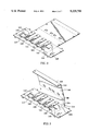
- FIG. 2 is an isometric view illustrating a transitional phase in the formation of a microwave combline filter from the blank of FIG. 1;
- FIG. 3 is an isometric view illustrating a transitional phase in the formation of a microwave combline filter from the blank of FIG. 1;
- FIG. 4 is an isometric view illustrating a transitional phase using capacitance and coupling tabs in the formation of a microwave combline filter from the blank of FIG. 1;
- FIG. 5 is an isometric view illustrating a transitional phase in the formation of a microwave combline filter from the blank of FIG. 1;
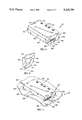
- FIG. 6 is an isometric view of a microwave combline filter embodiment formed from the blank of FIG. 1 in accordance with the present invention
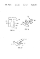
- FIG. 7 is an isometric view illustrating the microwave combline filter of FIG. 6 installed in a microstrip circuit
- FIG. 8 is an enlarged view of the area within the line 8 of FIG. 5;
- FIG. 9 is an enlarged view of the area within the line 9 of FIG. 6;
- FIG. 10 is an isometric view of another microwave combline filter embodiment in accordance with the present invention.
- FIG. 11 is an enlarged view of the area within the line 11 of FIG. 10;
- FIG. 12 is an isometric view of a microwave interdigital filter embodiment in accordance with the present invention.
- FIG. 13 is a view similar to FIG. 7 illustrating another filter embodiment in accordance with the present invention installed in a microstrip circuit
- FIG. 14 is a view similar to FIG. 7 illustrating another filter embodiment in accordance with the present invention installed in a microstrip circuit
- FIG. 15 is a plan view of another embodiment of a resonator portion of the blank of FIG. 1;
- FIG. 16 is an isometric view of another resonator embodiment formed of the resonator portion of FIG. 15;
- FIG. 17 is an isometric view of another embodiment of a tap portion of the blank of FIG. 1.
- the present invention is directed to a method for economically fabricating microwave filters and to the filters produced as a result thereof.
- the adjoining edges of the formed blank are bonded in a manner well known in the art (e.g. soldering or welding) to complete fabrication of the filter 30.
- the blank 20 may be fabricated by standard methods (e.g. stamping, etching, cutting, or laser milling) in sufficient numbers for a production run and economically stored until needed for assembly.
- the fabrication method used for the blank may also be used to simultaneously create bend lines such as bend line 36 in FIG. 1A by weakening the material therealong (e.g. partial removal of material or intermittent holes or slots). Forming of the blank 20 into the housing 22 is then reduced to simple bending along the bend lines.
- FIG. 1A is a plan view of a blank 20 fabricated from a sheet of electrically conductive material.
- the blank 20 defines portions which correspond, respectively, to housing elements and structural elements in the housing 22.
- the housing elements are housing walls, housing ends, resonators, resonator taps and grounding tabs.
- the structural elements are fingers, stops and resonator stiffening flaps.
- the blank 20 defines a peripheral edge 21 extending around a plurality of planar housing portions including wall portions 40, 42, 44, 46 and 48 and end portions 50 and 52.
- the planar portions, including leading and trailing wall portions 40 and 48, respectively, and intermediate wall portions 42, 44 and 46 are connected in series, separated by boundaries in the form of bend lines 36, 108, 110 and 112.
- Other intermediate wall portions 50 and 52 are contiguous with planar portion 42 at opposite ends thereof and respectively separated therefrom by bend lines 114, 116.
- portions 42 and 46 respectively form bottom and top walls
- portion 44 forms a rear wall
- portions 40 and 48 respectively form front upper and lower walls
- portions 50 and 52 form left and right end walls.
- each part of the peripheral edge 21 lies adjacent to another part of the peripheral edge.
- These adjacent edge parts are preferably sealed by a suitable procedure, e.g., soldering, so that the planar housing portions define a substantially closed internal cavity 23 (as shown in FIG. 6).
- extensions in the form of planar resonator portions 60, 62, 64 and 66 are formed integrally with the blank 20, extending outwardly from the peripheral edge 21, contiguous with planar portion 40 and respectively separated therefrom by boundaries in the form of bend lines 100, 102, 104 and 106.
- the height of rear wall portion 44 equals the sum of the heights of front upper and lower wall portions 40, 48.
- the extensions 60, 62, 64, and 66 bent perpendicular to the front lower wall portions 40, will project into the cavity 23 to be spaced from both the bottom and top wall portions 42, 46 and the rear wall portion 44.
- the height of front upper and lower wall portions 40, 48 are shown in FIGS. 1-6 to be substantially equal, it should be understood that the teachings of the invention include unequal heights which would cause the spacing between the extensions and bottom and top wall portions 42, 46 to also be unequal.
- the wall portions, end portions and extensions of the blank 20 in FIG. 1A correspond to the housing walls, ends and resonators of the housing 22 of FIG. 6.
- the tap portions 70, 72 and grounding tab portions 73 of the blank 20 correspond to the taps and grounding tabs of the housing 22.
- the tap portions 70, 72 extend from, and are contiguous with, respectively, resonator portions 60, 66.
- the grounding tab portions 73 are defined by each of the end portions 50, 52.
- the blank 20 has finger portions 76, stop portions 78 and flap portions 80 corresponding to the structural fingers, stops and flaps on the cavity 22.
- the blank 20 also defines notches 81, tuning holes 82, 84, 86 and 88 and apertures 90, 92.
- Bend lines 36, 100, 102, 104, 106, 108, 110, 112, 114, 116, 118 and 119 are defined in a manner similar to that described above relative to bend line 36.
- exemplary finger portions 76 and notches 81 are designated on FIG. 1.
- Four notches 81a have a function which differs from that of the notches 81. The function of both will be described in conjunction with FIG. 9.
- FIG. 1B illustrates another embodiment of the terminal resonator portions 60, 66 of blank 20.
- FIG. 1B is a view similar to the area within the line 1B of FIG. 1A showing a capacitance tap portion 70a contiguous with a resonator portion 60a in a blank 20a.
- the blank 20a is otherwise similar to the blank 20.
- Partition line 120 is defined in a manner similar to that described above relative to bend line 36. The purpose of partition line 120 will be described below.
- FIG. 1C illustrates another embodiment of the terminal resonator portions 60, 66 of blank 20.
- FIG. 1C is a view similar to FIG. 1B showing a coupling loop portion 70b contiguous with a wall portion 40b and adjacent a resonator portions 60b in a blank 20b.
- the coupling loop portion has a bend line 121.
- the blank 20b is otherwise similar to the blank 20.
- the bend line 121 is defined in a manner similar to that described above relative to bend line 36.
- the resonator portions 60, 62, 64 and 66 have been bent along bend lines 100, 102, 104 and 106 to form resonator elements 140, 142, 144 and 146 while wall portion 40 has been bent along bend line 108 to form a partial housing wall 147.
- Resonator tap portions 70, 72 have become, respectively, resonator taps 148, 149.
- wall portion 44 has been bent along bend line 110 to form housing walls 152 and 154
- wall portion 46 has been partially bent along bend line 36 to form housing wall 156
- wall portion 48 has been bent along bend line 112 to form partial wall 158.
- Partial walls 147 and 158 when joined, will form the housing wall opposite housing wall 154.
- the tuning bracket 24 has been bonded (e.g. soldered or welded) to the housing wall 154.
- the tuning bracket 24 has capacitance tabs 160, 162, 164, 166 and coupling tabs 171, 173, 175.
- Each capacitance tab is spaced above a corresponding resonator (e.g. capacitance tab 160 and resonator 140) and each coupling tab is spaced above and substantially equidistant from a corresponding pair of resonators (e.g. coupling tab 171 and resonators 140, 142).
- Capacitance tabs are used to adjust the capacitance of the resonators while coupling tabs are used to adjust the electromagnetic coupling between resonators by bending them in manners well known in the art. Access to each of the capacitance tabs and coupling tabs is gained through a corresponding one of the tuning holes 82, 84, 86 and 88 (e.g. access to capacitance tab 160 and coupling tab 171 is through tuning hole 82). These tuning elements (capacitance tabs and coupling tabs) facilitate adjustment of resonator capacitance and coupling between resonators to tune the transfer function of the filter (30 in FIG. 7).
- FIG. 5 the bend along bend line 36 has been completed so that partial housing walls 147 and 158 adjoin.
- end portions 50 and 52 have been bent along bend lines 114 and 116 to form, respectively, housing ends 178, 179 (wall 156 is broken away to show end 179).
- Resonator tap 148 now extends through aperture 90 (similarly, but not shown, resonator tap 149 extends through aperture 92).
- Grounding tab portions 73 are bent along bend lines (118 in FIG. 1A) to form grounding tabs 180. All adjoining housing wall and end edges are bonded to complete the fabrication of the housing 22 defining the cavity 23 therein.
- the filter 30, illustrated in FIG. 6, is comprised of only two elements, the housing 22 and the tuning bracket 24.
- the finger portions 76 become structural fingers 181 which are received in corresponding notches 81 as shown in FIG. 9 which is an enlarged view of the area enclosed by the line 9 in FIG. 6.
- the stop portions 78 of the blank 20 become stops 182 as shown in FIG. 9.
- the stops 182 fit into the notches 81a of the blank 20.
- the purpose of the stops 182 will be described below.
- the flap portions 80 of the blank 20 are bent relative to the resonators 140, 142, 144 and 146 along bend lines 119 as shown in FIG. 2 (designated on resonator 146) to become flaps 183 which add structural strength thereto.
- the end of each flap 183 nearest the partial wall 147 abuts therewith and the line of abutment is soldered for additional strength.
- the filter 30 is connected to a microstrip circuit 32.
- the stops 182 automatically align the resonator tap 148 along the microstrip line 186 when the filter 22 is dropped into a corresponding hole 188 in the circuit board 190 (similarly, but not shown, resonator tap 149 is aligned along microstrip line 187).
- the grounding tabs 180 are bonded to ground pads 192 of the microstrip circuit board 190.
- the ground pads 192 are electrically connected to the microstrip ground plane (far side of board 190) by suitable means (e.g. plated through holes).
- the resonator taps 148, 149 are bonded, respectively, to microstrip lines 186, 187 in manners well known in the art.
- FIG. 8 which is an enlarged view of the area enclosed by the line 8 of FIG. 5, illustrates that the blank 20 is bent away from areas 193 of removed material (described relative to bend line 36 above) that define the bend lines of FIG. 1A.
- the inner housing surface has a smooth transition between walls which prevents creation of electromagnetic discontinuities.
- FIG. 10 is a isometric view illustrating another embodiment of the capacitance and coupling adjustments shown in FIG. 4.
- Capacitance tips 230 terminate resonators 240, 242, 244, 246 and are bent relative thereto to adjust the capacitance thereof similar to the functioning of the capacitance tabs 160, 162, 164 and 166 of FIG. 4.
- the resonators extend from a wall 247.
- FIG. 11 is an enlarged view of the area enclosed by the line 11 of FIG. 10 and shows a slot 250 that facilitates bending of the capacitance tips 230.
- the slots 250 would be defined in a blank similar to the blank 20 of FIG. 1A.
- the housing wall 254 has coupling ears 271, 273 and 275 which may be used to adjust resonator coupling similar to tabs 171, 173 and 175 shown in FIG. 4.
- the ears 271, 273 and 275 would also be defined in a blank similar to the blank 20 of FIG. 1A.
- FIG. 12 is an isometric view similar to FIG. 4 illustrating another embodiment in which resonators 341 and 343 are interdigitated with resonators 340, 342 and 344 extending from the partial housing wall 347.
- the resonators 341 and 343 are defined on a resonator bracket 352 which mounts on housing wall 354.
- FIG. 13 is a view similar to FIG. 7 illustrating another filter embodiment installed in the microstrip circuit 32.
- the filter 30a has a capacitance tap 148a soldered to the microstrip line 186 in capacitive coupling association with the resonator 140a.
- the capacitance tap 148a and resonator 140a are formed from, respectively, the capacitance tap portion 70a and resonator portion 60a illustrated in FIG. 1B by breaking the capacitance tap portion 70a away from the resonator portion 60a along the partition line 120.
- a similar cavity coupling arrangement can be used to couple to the microstrip line 187.
- FIG. 14 is a view similar to FIG. 7 illustrating another filter embodiment installed in the microstrip circuit 32.
- the filter 30b has an inductance loop 148b soldered to the microstrip line 186 in inductive coupling association with the resonator 140b.
- the inductive loop 148b and resonator 140b are formed from, respectively, the inductive loop portion 70b and resonator portion 60b illustrated in FIG. 1C.
- the inductive loop portion 70b is bent along the bend line 121 (shown in FIG. 1C) to form the inductive loop 148b.
- a similar cavity coupling arrangement can be used to couple to the microstrip line 187.
- FIG. 15 is a plan view of another embodiment of a resonator portion 462 similar to the resonator portion 62 of FIG. 1A.
- the resonator portion 462 has sub-portions 463, 464, 465, 466 and 467.
- the resonator portion 462 is formed and bonded into the resonator embodiment 542 (similar to resonator 142) shown in FIG. 16 in which the location of the sub-portions is indicated.
- the resonator 542 may be bonded at its base to the housing wall 547.
- An impedance matching tab 630 extending from a tab embodiment 648 on a resonator 640 and a housing wall 647 is illustrated in the isometric view of FIG. 17.
- the tab 630 would be used to match the line impedance of a stripline circuit in which the resonator 640 would be integrated.
- the tab 630 would be defined in a blank similar to the blank 20 of FIG. 1A.
Abstract
Description
Claims (15)
Priority Applications (1)
| Application Number | Priority Date | Filing Date | Title |
|---|---|---|---|
| US07/977,306 US5225799A (en) | 1991-06-04 | 1992-11-16 | Microwave filter fabrication method and filters therefrom |
Applications Claiming Priority (2)
| Application Number | Priority Date | Filing Date | Title |
|---|---|---|---|
| US71009291A | 1991-06-04 | 1991-06-04 | |
| US07/977,306 US5225799A (en) | 1991-06-04 | 1992-11-16 | Microwave filter fabrication method and filters therefrom |
Related Parent Applications (1)
| Application Number | Title | Priority Date | Filing Date |
|---|---|---|---|
| US71009291A Continuation | 1991-06-04 | 1991-06-04 |
Publications (1)
| Publication Number | Publication Date |
|---|---|
| US5225799A true US5225799A (en) | 1993-07-06 |
Family
ID=27108372
Family Applications (1)
| Application Number | Title | Priority Date | Filing Date |
|---|---|---|---|
| US07/977,306 Expired - Fee Related US5225799A (en) | 1991-06-04 | 1992-11-16 | Microwave filter fabrication method and filters therefrom |
Country Status (1)
| Country | Link |
|---|---|
| US (1) | US5225799A (en) |
Cited By (41)
| Publication number | Priority date | Publication date | Assignee | Title |
|---|---|---|---|---|
| US5278527A (en) * | 1992-07-17 | 1994-01-11 | Motorola, Inc. | Dielectric filter and shield therefor |
| WO1996041395A1 (en) * | 1995-06-07 | 1996-12-19 | E-Systems, Inc. | Microwave packaging technique for integration of microwave filters and microwave cavity structures into microwave housings |
| US5666093A (en) * | 1995-08-11 | 1997-09-09 | D'ostilio; James Phillip | Mechanically tunable ceramic bandpass filter having moveable tabs |
| US5892419A (en) * | 1995-09-26 | 1999-04-06 | Adc Solitra Oy | Integral resonators for a filter and a method for manufacturing thereof |
| US6122482A (en) * | 1995-02-22 | 2000-09-19 | Global Communications, Inc. | Satellite broadcast receiving and distribution system |
| EP1091443A2 (en) * | 1999-10-04 | 2001-04-11 | Alps Electric Co., Ltd. | Satellite broadcast receiving converter |
| EP1143552A1 (en) * | 2000-03-09 | 2001-10-10 | Lucent Technologies Inc. | Sheet-metal filter |
| US6326920B1 (en) | 2000-03-09 | 2001-12-04 | Avaya Technology Corp. | Sheet-metal antenna |
| US6329949B1 (en) | 2000-03-09 | 2001-12-11 | Avaya Technology Corp. | Transceiver stacked assembly |
| WO2004012297A2 (en) * | 2002-07-29 | 2004-02-05 | Sage Laboratories, Inc. | Suspended-stripline hybrid coupler |
| US20040206152A1 (en) * | 2000-08-17 | 2004-10-21 | Durney Max W. | Sheet material with bend controlling displacements and method for forming the same |
| US20050005670A1 (en) * | 2000-08-17 | 2005-01-13 | Durney Max W. | Method of designing fold lines in sheet material |
| US20050030130A1 (en) * | 2003-07-31 | 2005-02-10 | Andrew Corporation | Method of manufacturing microwave filter components and microwave filter components formed thereby |
| US20050064138A1 (en) * | 2000-08-17 | 2005-03-24 | Durney Max W. | Method for precision bending of sheet of materials, slit sheets fabrication process |
| US20050097937A1 (en) * | 2000-08-17 | 2005-05-12 | Durney Max W. | Sheet material with bend controlling grooves defining a continuous web across a bend line and method for forming the same |
| US20050257589A1 (en) * | 2000-08-17 | 2005-11-24 | Industrial Origami, Llc | Sheet material with bend controlling displacements and method for forming the same |
| US20060021413A1 (en) * | 2000-08-17 | 2006-02-02 | Durney Max W | Fatigue-resistance sheet slitting method and resulting sheet |
| US20060207212A1 (en) * | 2000-08-17 | 2006-09-21 | Industrial Origami, Llc | Precision-folded, high strength, fatigue-resistant structures and sheet therefor |
| US20060213245A1 (en) * | 2000-08-17 | 2006-09-28 | Industrial Origami, Llc | Method and tooling for forming sheet material with bend controlling displacements |
| US20060261139A1 (en) * | 2000-08-17 | 2006-11-23 | Industrial Origami, Llc | Apparatus and method for joining the edges of folded sheet material to form three-dimensional structure |
| US7222511B2 (en) | 2000-08-17 | 2007-05-29 | Industrial Origami, Inc. | Process of forming bend-controlling structures in a sheet of material, the resulting sheet and die sets therefor |
| US7354639B2 (en) | 2004-12-16 | 2008-04-08 | Industrial Origami, Inc. | Method of bending sheet materials and sheet therefor |
| US20080293477A1 (en) * | 2005-04-27 | 2008-11-27 | Aruze Corp. | Gaming machine |
| CN1838476B (en) * | 2005-03-24 | 2010-04-28 | 华为技术有限公司 | Suspended mictrostrip filter and duplexer and method for designing and debugging filter |
| US20100122563A1 (en) * | 2008-11-16 | 2010-05-20 | Industrial Origami, Inc. | Method and apparatus for forming bend-controlling straps in sheet material |
| US20110121918A1 (en) * | 2006-08-31 | 2011-05-26 | Minoru Tachibana | Filter device and method for manufacturing the same |
| US8438893B2 (en) | 2006-10-26 | 2013-05-14 | Industrial Origami, Inc. | Method of forming two-dimensional sheet material into three-dimensional structure |
| US8505258B2 (en) | 2000-08-17 | 2013-08-13 | Industrial Origami, Inc. | Load-bearing three-dimensional structure |
| US8834337B2 (en) | 2010-06-07 | 2014-09-16 | Robert Joseph Hannum | Method of folding sheet materials via angled torsional strips |
| US8936164B2 (en) | 2012-07-06 | 2015-01-20 | Industrial Origami, Inc. | Solar panel rack |
| US9190707B2 (en) * | 2011-10-18 | 2015-11-17 | Prism Microwave, Inc. | Method for manufacturing an RF filter and an RF filter |
| WO2015177411A1 (en) * | 2014-05-23 | 2015-11-26 | Prism Microwave Oy | Rf filter |
| WO2015177412A1 (en) * | 2014-05-23 | 2015-11-26 | Prism Microwave Oy | Tuning element for radio frequency resonator |
| CN109428140A (en) * | 2017-08-30 | 2019-03-05 | 凯瑟雷恩欧洲股份公司 | Coaxial filter |
| US20190296412A1 (en) * | 2016-12-09 | 2019-09-26 | Huawei Technologies Co., Ltd. | Filtering device |
| EP3667810A1 (en) * | 2018-12-14 | 2020-06-17 | CommScope Italy S.r.l. | Filters having resonators with negative coupling |
| WO2021155424A1 (en) * | 2020-02-07 | 2021-08-12 | Roy Tiles Pty Limited | Handle attachment for an adhesive spreader |
| EP3797447A4 (en) * | 2018-06-04 | 2022-01-05 | Nokia Solutions and Networks Oy | A cavity filter |
| WO2023208759A1 (en) * | 2022-04-28 | 2023-11-02 | Commscope Italy S.R.L. | Radio frequency filters covered by feed boards |
| WO2023220971A1 (en) * | 2022-05-18 | 2023-11-23 | Telefonaktiebolaget Lm Ericsson (Publ) | Filter and communication device having the same |
| EP4304002A1 (en) * | 2022-07-05 | 2024-01-10 | Solexy S.R.L. Uninominale | A multichannel connector for safe areas, a filtering group for a multichannel connector, and an explosion-proof box |
Citations (2)
| Publication number | Priority date | Publication date | Assignee | Title |
|---|---|---|---|---|
| US4829274A (en) * | 1986-07-25 | 1989-05-09 | Motorola, Inc. | Multiple resonator dielectric filter |
| US5079528A (en) * | 1989-06-21 | 1992-01-07 | Murata Manufacturing Co. Ltd. | Dielectric filter |
-
1992
- 1992-11-16 US US07/977,306 patent/US5225799A/en not_active Expired - Fee Related
Patent Citations (2)
| Publication number | Priority date | Publication date | Assignee | Title |
|---|---|---|---|---|
| US4829274A (en) * | 1986-07-25 | 1989-05-09 | Motorola, Inc. | Multiple resonator dielectric filter |
| US5079528A (en) * | 1989-06-21 | 1992-01-07 | Murata Manufacturing Co. Ltd. | Dielectric filter |
Cited By (105)
| Publication number | Priority date | Publication date | Assignee | Title |
|---|---|---|---|---|
| US5278527A (en) * | 1992-07-17 | 1994-01-11 | Motorola, Inc. | Dielectric filter and shield therefor |
| WO1994002971A1 (en) * | 1992-07-17 | 1994-02-03 | Motorola Inc. | Dielectric filter and shield therefor |
| GB2274550A (en) * | 1992-07-17 | 1994-07-27 | Motorola Inc | Dielectric filter and shield therefor |
| GB2274550B (en) * | 1992-07-17 | 1995-11-29 | Motorola Inc | Dielectric filter and shield therefor |
| US6397038B1 (en) | 1995-02-22 | 2002-05-28 | Global Communications, Inc. | Satellite broadcast receiving and distribution system |
| US20110197235A1 (en) * | 1995-02-22 | 2011-08-11 | Global Communications, Inc. | Satellite broadcast receiving and distribution system |
| US6917783B2 (en) | 1995-02-22 | 2005-07-12 | Global Communications, Inc. | Satellite broadcast receiving and distribution system |
| US6122482A (en) * | 1995-02-22 | 2000-09-19 | Global Communications, Inc. | Satellite broadcast receiving and distribution system |
| US6947702B2 (en) | 1995-02-22 | 2005-09-20 | Global Communications, Inc. | Satellite broadcast receiving and distribution system |
| US20050221756A1 (en) * | 1995-02-22 | 2005-10-06 | Global Communications, Inc. | Satellite broadcast receiving and distribution system |
| US7542717B2 (en) | 1995-02-22 | 2009-06-02 | Global Communications, Inc. | Satellite broadcast receiving and distribution system |
| US20090282442A1 (en) * | 1995-02-22 | 2009-11-12 | Global Communications, Inc. | Satellite broadcast receiving and distribution system |
| US6334045B1 (en) | 1995-02-22 | 2001-12-25 | Global Communications, Inc. | Satellite broadcast receiving and distribution system |
| US7826791B2 (en) | 1995-02-22 | 2010-11-02 | Global Communications, Inc. | Satellite broadcast receiving and distribution system |
| US20050176365A1 (en) * | 1995-02-22 | 2005-08-11 | Global Communications, Inc. | Satellite broadcast receiving and distribution system |
| US8095064B2 (en) | 1995-02-22 | 2012-01-10 | Global Communications, Inc. | Satellite broadcast receiving and distribution system |
| US20020094775A1 (en) * | 1995-02-22 | 2002-07-18 | Global Communications, Inc. | Satellite broadcast receiving and distribution system |
| US20030040270A1 (en) * | 1995-02-22 | 2003-02-27 | Global Communications, Inc. | Satellite broadcast receiving and distribution system |
| US8165520B2 (en) | 1995-02-22 | 2012-04-24 | Global Communications, Inc. | Satellite broadcast receiving and distribution system |
| US8666307B2 (en) | 1995-02-22 | 2014-03-04 | Global Communications, Inc. | Satellite broadcast receiving and distribution system |
| US8583029B2 (en) | 1995-02-22 | 2013-11-12 | Global Communications, Inc. | Satellite broadcast receiving and distribution system |
| WO1996041395A1 (en) * | 1995-06-07 | 1996-12-19 | E-Systems, Inc. | Microwave packaging technique for integration of microwave filters and microwave cavity structures into microwave housings |
| US5666093A (en) * | 1995-08-11 | 1997-09-09 | D'ostilio; James Phillip | Mechanically tunable ceramic bandpass filter having moveable tabs |
| US5892419A (en) * | 1995-09-26 | 1999-04-06 | Adc Solitra Oy | Integral resonators for a filter and a method for manufacturing thereof |
| US6658233B1 (en) | 1999-10-04 | 2003-12-02 | Alps Electric Co., Ltd. | Satellite broadcast receiving converter |
| EP1091443A3 (en) * | 1999-10-04 | 2002-07-03 | Alps Electric Co., Ltd. | Satellite broadcast receiving converter |
| EP1091443A2 (en) * | 1999-10-04 | 2001-04-11 | Alps Electric Co., Ltd. | Satellite broadcast receiving converter |
| US6356168B1 (en) | 2000-03-09 | 2002-03-12 | Avaya Technology Corp. | Sheet-metal filter |
| US6329949B1 (en) | 2000-03-09 | 2001-12-11 | Avaya Technology Corp. | Transceiver stacked assembly |
| US6326920B1 (en) | 2000-03-09 | 2001-12-04 | Avaya Technology Corp. | Sheet-metal antenna |
| EP1143552A1 (en) * | 2000-03-09 | 2001-10-10 | Lucent Technologies Inc. | Sheet-metal filter |
| US7412865B2 (en) | 2000-08-17 | 2008-08-19 | Industrial Origami, Inc. | Method for forming sheet material with bend controlling displacements |
| US7640775B2 (en) | 2000-08-17 | 2010-01-05 | Industrial Origami, Inc. | Apparatus and method for joining the edges of folded sheet material to form three-dimensional structure |
| US8505258B2 (en) | 2000-08-17 | 2013-08-13 | Industrial Origami, Inc. | Load-bearing three-dimensional structure |
| US20050257589A1 (en) * | 2000-08-17 | 2005-11-24 | Industrial Origami, Llc | Sheet material with bend controlling displacements and method for forming the same |
| US20060021413A1 (en) * | 2000-08-17 | 2006-02-02 | Durney Max W | Fatigue-resistance sheet slitting method and resulting sheet |
| US20060075798A1 (en) * | 2000-08-17 | 2006-04-13 | Industrial Origami, Llc | Sheet material with bend controlling displacements and method for forming the same |
| US7032426B2 (en) | 2000-08-17 | 2006-04-25 | Industrial Origami, Llc | Techniques for designing and manufacturing precision-folded, high strength, fatigue-resistant structures and sheet therefor |
| US20060207212A1 (en) * | 2000-08-17 | 2006-09-21 | Industrial Origami, Llc | Precision-folded, high strength, fatigue-resistant structures and sheet therefor |
| US20060213245A1 (en) * | 2000-08-17 | 2006-09-28 | Industrial Origami, Llc | Method and tooling for forming sheet material with bend controlling displacements |
| US20060261139A1 (en) * | 2000-08-17 | 2006-11-23 | Industrial Origami, Llc | Apparatus and method for joining the edges of folded sheet material to form three-dimensional structure |
| US7152450B2 (en) | 2000-08-17 | 2006-12-26 | Industrial Origami, Llc | Method for forming sheet material with bend controlling displacements |
| US7152449B2 (en) | 2000-08-17 | 2006-12-26 | Industrial Origami, Llc | Techniques for designing and manufacturing precision-folded, high strength, fatigue-resistant structures and sheet therefor |
| US7222511B2 (en) | 2000-08-17 | 2007-05-29 | Industrial Origami, Inc. | Process of forming bend-controlling structures in a sheet of material, the resulting sheet and die sets therefor |
| US7263869B2 (en) | 2000-08-17 | 2007-09-04 | Industrial Origami, Inc. | Method for forming sheet material with bend controlling grooves defining a continuous web across a bend line |
| US20080016937A1 (en) * | 2000-08-17 | 2008-01-24 | Industrial Origami, Inc | Process of forming bend-controlling structures in a sheet of material, the resulting sheet and die sets therefor |
| US20080063834A1 (en) * | 2000-08-17 | 2008-03-13 | Industrial Origami, Inc. | Sheet Material with Bend Controlling Grooves Defining a Continuous Web Across a Bend Line and Method for Forming the Same |
| US7350390B2 (en) | 2000-08-17 | 2008-04-01 | Industrial Origami, Inc. | Sheet material with bend controlling displacements and method for forming the same |
| US20040206152A1 (en) * | 2000-08-17 | 2004-10-21 | Durney Max W. | Sheet material with bend controlling displacements and method for forming the same |
| US7374810B2 (en) | 2000-08-17 | 2008-05-20 | Industrial Origami, Inc. | Method for precision bending of sheet of materials, slit sheets fabrication process |
| US20080121009A1 (en) * | 2000-08-17 | 2008-05-29 | Industrial Origami, Inc. | Sheet material with bend controlling displacements and method for forming the same |
| US20080193714A1 (en) * | 2000-08-17 | 2008-08-14 | Industrial Origami, Inc. | Method for precision bending of sheet of materials, slit sheets fabrication process |
| US20050097937A1 (en) * | 2000-08-17 | 2005-05-12 | Durney Max W. | Sheet material with bend controlling grooves defining a continuous web across a bend line and method for forming the same |
| US7440874B2 (en) | 2000-08-17 | 2008-10-21 | Industrial Origami, Inc. | Method of designing fold lines in sheet material |
| US20050126110A1 (en) * | 2000-08-17 | 2005-06-16 | Durney Max W. | Techniques for designing and manufacturing precision-folded, high strength, fatigue-resistant structures and sheet therefor |
| US20080271511A1 (en) * | 2000-08-17 | 2008-11-06 | Industrial Origami, Inc. | Sheet material with bend controlling displacements and method for forming the same |
| US20050005670A1 (en) * | 2000-08-17 | 2005-01-13 | Durney Max W. | Method of designing fold lines in sheet material |
| US7464574B2 (en) | 2000-08-17 | 2008-12-16 | Industrial Origami, Inc. | Method for forming sheet material with bend facilitating structures into a fatigue resistant structure |
| US7534501B2 (en) | 2000-08-17 | 2009-05-19 | Industrial Origami, Inc. | Precision-folded, high strength, fatigue-resistant structures and sheet therefor |
| US6877349B2 (en) | 2000-08-17 | 2005-04-12 | Industrial Origami, Llc | Method for precision bending of sheet of materials, slit sheets fabrication process |
| US7560155B2 (en) | 2000-08-17 | 2009-07-14 | Industrial Origami, Inc. | Sheet material with bend controlling grooves defining a continuous web across a bend line and method for forming the same |
| US20050064138A1 (en) * | 2000-08-17 | 2005-03-24 | Durney Max W. | Method for precision bending of sheet of materials, slit sheets fabrication process |
| US7643967B2 (en) | 2000-08-17 | 2010-01-05 | Industrial Original, Inc. | Method of designing fold lines in sheet material |
| US6822532B2 (en) | 2002-07-29 | 2004-11-23 | Sage Laboratories, Inc. | Suspended-stripline hybrid coupler |
| WO2004012297A3 (en) * | 2002-07-29 | 2004-06-10 | Sage Laboratories | Suspended-stripline hybrid coupler |
| WO2004012297A2 (en) * | 2002-07-29 | 2004-02-05 | Sage Laboratories, Inc. | Suspended-stripline hybrid coupler |
| US8377566B2 (en) | 2002-09-26 | 2013-02-19 | Industrial Origami, Inc. | Precision-folded, high strength, fatigue-resistant structures and sheet therefor |
| US20050030130A1 (en) * | 2003-07-31 | 2005-02-10 | Andrew Corporation | Method of manufacturing microwave filter components and microwave filter components formed thereby |
| US6904666B2 (en) | 2003-07-31 | 2005-06-14 | Andrew Corporation | Method of manufacturing microwave filter components and microwave filter components formed thereby |
| US20080257006A1 (en) * | 2004-12-16 | 2008-10-23 | Industrial Origami, Inc. | Method of bending sheet materials and sheet therefor |
| US7354639B2 (en) | 2004-12-16 | 2008-04-08 | Industrial Origami, Inc. | Method of bending sheet materials and sheet therefor |
| CN1838476B (en) * | 2005-03-24 | 2010-04-28 | 华为技术有限公司 | Suspended mictrostrip filter and duplexer and method for designing and debugging filter |
| US20080293477A1 (en) * | 2005-04-27 | 2008-11-27 | Aruze Corp. | Gaming machine |
| US20110121918A1 (en) * | 2006-08-31 | 2011-05-26 | Minoru Tachibana | Filter device and method for manufacturing the same |
| US8438893B2 (en) | 2006-10-26 | 2013-05-14 | Industrial Origami, Inc. | Method of forming two-dimensional sheet material into three-dimensional structure |
| US20100122563A1 (en) * | 2008-11-16 | 2010-05-20 | Industrial Origami, Inc. | Method and apparatus for forming bend-controlling straps in sheet material |
| US8834337B2 (en) | 2010-06-07 | 2014-09-16 | Robert Joseph Hannum | Method of folding sheet materials via angled torsional strips |
| US9190707B2 (en) * | 2011-10-18 | 2015-11-17 | Prism Microwave, Inc. | Method for manufacturing an RF filter and an RF filter |
| US9425731B2 (en) | 2012-07-06 | 2016-08-23 | Industrial Origami, Inc. | Solar panel rack |
| US8936164B2 (en) | 2012-07-06 | 2015-01-20 | Industrial Origami, Inc. | Solar panel rack |
| US9166521B2 (en) * | 2012-07-06 | 2015-10-20 | Industrial Origami, Inc. | Solar panel rack |
| EP3146590A4 (en) * | 2014-05-23 | 2018-01-24 | Tongyu Technology Oy | Rf filter |
| CN106463806B (en) * | 2014-05-23 | 2020-03-27 | 通玉科技有限公司 | RF filter |
| CN106463806A (en) * | 2014-05-23 | 2017-02-22 | 通玉科技有限公司 | Rf filter |
| WO2015177411A1 (en) * | 2014-05-23 | 2015-11-26 | Prism Microwave Oy | Rf filter |
| EP3146589A4 (en) * | 2014-05-23 | 2018-01-24 | Tongyu Technology Oy | Tuning element for radio frequency resonator |
| US10056666B2 (en) | 2014-05-23 | 2018-08-21 | Tongyu Technology Oy | Tuning element for radio frequency resonator |
| WO2015177412A1 (en) * | 2014-05-23 | 2015-11-26 | Prism Microwave Oy | Tuning element for radio frequency resonator |
| US11664563B2 (en) | 2016-12-09 | 2023-05-30 | Huawei Technologies Co., Ltd. | Filtering device |
| US20190296412A1 (en) * | 2016-12-09 | 2019-09-26 | Huawei Technologies Co., Ltd. | Filtering device |
| US11043724B2 (en) * | 2016-12-09 | 2021-06-22 | Huawei Technologies Co., Ltd. | Filtering device |
| EP3451441A1 (en) * | 2017-08-30 | 2019-03-06 | Kathrein SE | Coaxial filter |
| CN109428140A (en) * | 2017-08-30 | 2019-03-05 | 凯瑟雷恩欧洲股份公司 | Coaxial filter |
| US11245167B2 (en) | 2017-08-30 | 2022-02-08 | Telefonaktiebolaget Lm Ericsson (Publ) | Coaxial filter |
| EP3797447A4 (en) * | 2018-06-04 | 2022-01-05 | Nokia Solutions and Networks Oy | A cavity filter |
| CN111326837A (en) * | 2018-12-14 | 2020-06-23 | 康普公司意大利有限责任公司 | Filter with resonators having negative coupling |
| CN111326837B (en) * | 2018-12-14 | 2021-12-17 | 康普公司意大利有限责任公司 | Filter with resonators having negative coupling |
| US11223094B2 (en) | 2018-12-14 | 2022-01-11 | Commscope Italy S.R.L. | Filters having resonators with negative coupling |
| CN114221101A (en) * | 2018-12-14 | 2022-03-22 | 康普公司意大利有限责任公司 | Filter with resonators having negative coupling |
| EP3667810A1 (en) * | 2018-12-14 | 2020-06-17 | CommScope Italy S.r.l. | Filters having resonators with negative coupling |
| US11721878B2 (en) | 2018-12-14 | 2023-08-08 | Commscope Italy S.R.L. | Filters having resonators with negative coupling |
| WO2021155424A1 (en) * | 2020-02-07 | 2021-08-12 | Roy Tiles Pty Limited | Handle attachment for an adhesive spreader |
| WO2023208759A1 (en) * | 2022-04-28 | 2023-11-02 | Commscope Italy S.R.L. | Radio frequency filters covered by feed boards |
| WO2023220971A1 (en) * | 2022-05-18 | 2023-11-23 | Telefonaktiebolaget Lm Ericsson (Publ) | Filter and communication device having the same |
| EP4304002A1 (en) * | 2022-07-05 | 2024-01-10 | Solexy S.R.L. Uninominale | A multichannel connector for safe areas, a filtering group for a multichannel connector, and an explosion-proof box |
Similar Documents
| Publication | Publication Date | Title |
|---|---|---|
| US5225799A (en) | Microwave filter fabrication method and filters therefrom | |
| EP0706230B1 (en) | Radio frequency filter comprising helix resonators | |
| US6225959B1 (en) | Dual frequency cavity backed slot antenna | |
| EP0520673A1 (en) | A dielectric filter | |
| US5343176A (en) | Radio frequency filter having a substrate with recessed areas | |
| EP0563987B1 (en) | Dielectric filters mounted on a substrate for carrying input and output striplines | |
| US5218330A (en) | Apparatus and method for easily adjusting the resonant frequency of a dielectric TEM resonator | |
| JPH10233604A (en) | High frequency filter | |
| CN212209713U (en) | Metal sheet radio frequency cavity filter | |
| US5214398A (en) | Dielectric filter coupling structure having a compact terminal arrangement | |
| WO1992022101A1 (en) | Microwave filter fabrication method and filters therefrom | |
| CN212303856U (en) | Metal sheet radio frequency cavity filter | |
| WO1994002971A1 (en) | Dielectric filter and shield therefor | |
| JP2003115701A (en) | High frequency filter | |
| US5831495A (en) | Dielectric filter including laterally extending auxiliary through bores | |
| US6150905A (en) | Dielectric filter with through-hole having large and small diameter portions and a coupling adjustment portion | |
| EP1324419B1 (en) | System for cross-coupling resonators | |
| JPS6029203Y2 (en) | Narrowband high frequency resonator | |
| EP0838875B1 (en) | Dielectric filter | |
| JPH0158881B2 (en) | ||
| KR20240038616A (en) | Filter for communication device | |
| US20230006323A1 (en) | Radio frequency filters having a circuit board with multiple resonator heads, and resonator heads having multiple arms | |
| JP2661006B2 (en) | Dielectric filter | |
| US5859575A (en) | Dielectric filter | |
| JPS63299607A (en) | Surface packing type band pass filter |
Legal Events
| Date | Code | Title | Description |
|---|---|---|---|
| REMI | Maintenance fee reminder mailed | ||
| FPAY | Fee payment |
Year of fee payment: 4 |
|
| SULP | Surcharge for late payment | ||
| FPAY | Fee payment |
Year of fee payment: 8 |
|
| AS | Assignment |
Owner name: U.S. BANK NATIONAL ASSOCIATION, CALIFORNIA Free format text: SECURITY INTEREST;ASSIGNOR:CALIFORNIA AMPLIFIER, INC.;REEL/FRAME:012916/0651 Effective date: 20020502 |
|
| REMI | Maintenance fee reminder mailed | ||
| REMI | Maintenance fee reminder mailed | ||
| AS | Assignment |
Owner name: CALAMP CORP., CALIFORNIA Free format text: CHANGE OF NAME;ASSIGNOR:CALIFORNIA AMPLIFIER, INC.;REEL/FRAME:016309/0949 Effective date: 20040730 |
|
| LAPS | Lapse for failure to pay maintenance fees | ||
| STCH | Information on status: patent discontinuation |
Free format text: PATENT EXPIRED DUE TO NONPAYMENT OF MAINTENANCE FEES UNDER 37 CFR 1.362 |
|
| FP | Lapsed due to failure to pay maintenance fee |
Effective date: 20050706 |
|
| AS | Assignment |
Owner name: U.S. BANK NATIONAL ASSOCIATION, OREGON Free format text: RELEASE;ASSIGNOR:CALIFORNIA AMPLIFIER, INC.;REEL/FRAME:018160/0382 Effective date: 20060530 |
|
| AS | Assignment |
Owner name: PACIFIC WESTERN BANK, NORTH CAROLINA Free format text: SECURITY INTEREST;ASSIGNOR:CALAMP CORP.;REEL/FRAME:038789/0183 Effective date: 20160527 |
|
| AS | Assignment |
Owner name: CALAMP CORP., CALIFORNIA Free format text: RELEASE BY SECURED PARTY;ASSIGNOR:PACIFIC WESTERN BANK;REEL/FRAME:044275/0347 Effective date: 20171025 |
|
| AS | Assignment |
Owner name: JPMORGAN CHASE BANK, N.A., NEW YORK Free format text: SECURITY INTEREST;ASSIGNOR:CALAMP CORP.;REEL/FRAME:045853/0023 Effective date: 20180330 |