US5226823A - Indexing mechanism for precision alignment of electrical contacts - Google Patents
Indexing mechanism for precision alignment of electrical contacts Download PDFInfo
- Publication number
- US5226823A US5226823A US07/819,081 US81908192A US5226823A US 5226823 A US5226823 A US 5226823A US 81908192 A US81908192 A US 81908192A US 5226823 A US5226823 A US 5226823A
- Authority
- US
- United States
- Prior art keywords
- substrate
- connector
- contact pads
- connector contacts
- frame
- Prior art date
- Legal status (The legal status is an assumption and is not a legal conclusion. Google has not performed a legal analysis and makes no representation as to the accuracy of the status listed.)
- Expired - Lifetime
Links
Images


Classifications
-
- H—ELECTRICITY
- H05—ELECTRIC TECHNIQUES NOT OTHERWISE PROVIDED FOR
- H05K—PRINTED CIRCUITS; CASINGS OR CONSTRUCTIONAL DETAILS OF ELECTRIC APPARATUS; MANUFACTURE OF ASSEMBLAGES OF ELECTRICAL COMPONENTS
- H05K7/00—Constructional details common to different types of electric apparatus
- H05K7/02—Arrangements of circuit components or wiring on supporting structure
- H05K7/023—Stackable modules
-
- H—ELECTRICITY
- H01—ELECTRIC ELEMENTS
- H01R—ELECTRICALLY-CONDUCTIVE CONNECTIONS; STRUCTURAL ASSOCIATIONS OF A PLURALITY OF MUTUALLY-INSULATED ELECTRICAL CONNECTING ELEMENTS; COUPLING DEVICES; CURRENT COLLECTORS
- H01R12/00—Structural associations of a plurality of mutually-insulated electrical connecting elements, specially adapted for printed circuits, e.g. printed circuit boards [PCB], flat or ribbon cables, or like generally planar structures, e.g. terminal strips, terminal blocks; Coupling devices specially adapted for printed circuits, flat or ribbon cables, or like generally planar structures; Terminals specially adapted for contact with, or insertion into, printed circuits, flat or ribbon cables, or like generally planar structures
- H01R12/50—Fixed connections
- H01R12/51—Fixed connections for rigid printed circuits or like structures
- H01R12/52—Fixed connections for rigid printed circuits or like structures connecting to other rigid printed circuits or like structures
-
- H—ELECTRICITY
- H01—ELECTRIC ELEMENTS
- H01R—ELECTRICALLY-CONDUCTIVE CONNECTIONS; STRUCTURAL ASSOCIATIONS OF A PLURALITY OF MUTUALLY-INSULATED ELECTRICAL CONNECTING ELEMENTS; COUPLING DEVICES; CURRENT COLLECTORS
- H01R12/00—Structural associations of a plurality of mutually-insulated electrical connecting elements, specially adapted for printed circuits, e.g. printed circuit boards [PCB], flat or ribbon cables, or like generally planar structures, e.g. terminal strips, terminal blocks; Coupling devices specially adapted for printed circuits, flat or ribbon cables, or like generally planar structures; Terminals specially adapted for contact with, or insertion into, printed circuits, flat or ribbon cables, or like generally planar structures
- H01R12/70—Coupling devices
- H01R12/7005—Guiding, mounting, polarizing or locking means; Extractors
-
- H—ELECTRICITY
- H01—ELECTRIC ELEMENTS
- H01R—ELECTRICALLY-CONDUCTIVE CONNECTIONS; STRUCTURAL ASSOCIATIONS OF A PLURALITY OF MUTUALLY-INSULATED ELECTRICAL CONNECTING ELEMENTS; COUPLING DEVICES; CURRENT COLLECTORS
- H01R12/00—Structural associations of a plurality of mutually-insulated electrical connecting elements, specially adapted for printed circuits, e.g. printed circuit boards [PCB], flat or ribbon cables, or like generally planar structures, e.g. terminal strips, terminal blocks; Coupling devices specially adapted for printed circuits, flat or ribbon cables, or like generally planar structures; Terminals specially adapted for contact with, or insertion into, printed circuits, flat or ribbon cables, or like generally planar structures
- H01R12/70—Coupling devices
- H01R12/71—Coupling devices for rigid printing circuits or like structures
- H01R12/712—Coupling devices for rigid printing circuits or like structures co-operating with the surface of the printed circuit or with a coupling device exclusively provided on the surface of the printed circuit
- H01R12/714—Coupling devices for rigid printing circuits or like structures co-operating with the surface of the printed circuit or with a coupling device exclusively provided on the surface of the printed circuit with contacts abutting directly the printed circuit; Button contacts therefore provided on the printed circuit
-
- H—ELECTRICITY
- H01—ELECTRIC ELEMENTS
- H01R—ELECTRICALLY-CONDUCTIVE CONNECTIONS; STRUCTURAL ASSOCIATIONS OF A PLURALITY OF MUTUALLY-INSULATED ELECTRICAL CONNECTING ELEMENTS; COUPLING DEVICES; CURRENT COLLECTORS
- H01R13/00—Details of coupling devices of the kinds covered by groups H01R12/70 or H01R24/00 - H01R33/00
- H01R13/02—Contact members
- H01R13/22—Contacts for co-operating by abutting
- H01R13/24—Contacts for co-operating by abutting resilient; resiliently-mounted
Definitions
- the invention relates to a method and apparatus for electrically connecting a plurality of electronic substrates and more particularly to a method and apparatus for electrically connecting a plurality of electronic substrates in an assembly of stackable connectors.
- Stackable connectors having a plurality of electrical contacts are commonly employed to electrically connect electronic substrates.
- One such stackable connector is disclosed in U.S. Pat. No. 4,395,084 to Conrad.
- the effectiveness of a stackable connector is dependent on the integrity of the electrical connection it provides. Torsional forces on a stackable connector can cause the electrical contacts of the connector to misalign with respect to the electrical contacts of the substrate. The problem is particularly acute when the contacts of several substrates and connectors, stacked in a single assembly are misaligned creating significant tolerance accumulation. The problem is manifested in poor electrical connections or even total loss of electrical connections.
- a method and apparatus are needed to enhance the integrity of the electrical connection between electronic substrates.
- a method and apparatus are needed to provide precision alignment between the electrical contacts of an electronic substrate and the electrical contacts of a stackable connector employed to electrically connect the substrate with other substrates.
- a method and apparatus are needed to provide precision alignment between the electrical contacts of a plurality of stackable connectors and the electrical contacts of a plurality of electronic substrates stacked together in a unitary assembly.
- the present invention is a method and apparatus for providing a reliable electrical connection between an electronic substrate and a stackable connector. Further, the present invention provides for precision alignment between a plurality of electronic substrates and a plurality of such bodies stacked together in a unitary assembly. Stated differently, the present invention provides for precision alignment between the electrical contacts of first and second electronic substrates and the electrical contacts of a connector positioned between the two substrates. As implied, a third electronic substrate may subsequently be electrically connected to the second electronic substrate by positioning a second connector therebetween and aligning the electrical contacts of the second and third substrates with the contacts of the second connector. Ultimately, as many electronic substrates as desired may be stacked in an assembly of connectors and electrically connected using the present invention. The invention is particularly useful for minimizing tolerance accumulation in an assembly having a relatively large number of stackable connectors and substrates housed therein.
- the apparatus of the present invention includes an indexing mechanism comprising a post associated with a stackable connector and a notch formed in a substrate.
- the notch is provided in the substrate to receive the post when the substrate is stacked against the connector.
- placement of the post in the notch automatically indexes the electrical contacts of the connector with the electrical contacts of the substrate.
- the post is an elongated member extending from a body which slidably engages a rail integral to the frame of the connector.
- the notch is an indentation in the substrate, and more specifically, a recess formed peripherally in the substrate surface.
- the substrate supports electrical contacts arranged on its surface which engage the electrical contacts of the connector body when the substrate is secured to the connector.
- the post and notch are positioned on the body and substrate respectively so that the post aligns with and fits closely with the notch when the substrate is properly positioned in an assembly of connectors and substrates. Placement of the post in the notch results in a precision alignment between the electrical contacts of the connector and substrate in the assembly. Thus, the integrity of the electrical connection between electronic substrates connected across the assembly is ensured when the indexing mechanism is utilized.
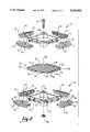
- FIG. 1 is a perspective view of an assembly of stackable connectors and substrates having the indexing mechanism of the present invention
- FIG. 2 is an exploded perspective view of an assembly housing a single substrate
- FIG. 3 is a side elevation view of the unitary assembly shown in FIG. 2;
- FIG. 4 is a cross-sectional view of the connector body showing both the stressed and unstressed conditions thereof.
- FIG. 5 is a side elevation view of an embodiment of the assembly having contact gaps provided therein.
- FIGS. 1 through 3 show a plurality of indexing mechanisms as they are employed in conjunction with a stacked assembly of connectors and substrates generally designated 10.
- each indexing mechanism comprises an upward post 40 or a downward post 42 which is associated with stackable connector 29, 30, 31, or 32, and further comprises a notch 14 which is associated With a substrate 28.
- Posts 40, 42 and notches 14 are designed to closely engage each other when substrate 28 and stackable connectors 29, 30, 31, 32 are secured in assembly 10.
- the term substrate refers generally to any substantially planar medium having electrical components mounted thereon, such as a leadless integrated circuit, a printed circuit board, or other such substrates known in the art.
- posts 40, 42 are mounted on a body 16 which is detachably affixable to frame 33b of connector 30 by means of a rail 20 provided on the outer edge 12 of frame 33b.
- Body 16 also has electrical connector contacts 22 mounted thereto.
- Body 16 is provided with a plurality of windows 60 in its surface to enable electrical access to each connector contact 22 through body 16. It is apparent that this description applies likewise to frame 33a of connector 29.
- Connector contacts 22 are a series of thin and resilient conductive metal strips which are molded directly into the structure of body 16. Connector contacts 22 are oriented substantially away from the axis of body 16 and are initially in an unstressed condition as shown by the solid line in FIG. 4. Unstressed connector contacts 22 are also shown positioned on the upper side of connector 29 and the lower side of connector 30 in FIG. 3.
- connector contacts 22 When body 16 is incorporated into stacking assembly 10 and connector contacts 22 engage upper contacts 26 and lower contacts 18 of substrate 28 in a manner described hereafter, connector contacts 22 assume a stressed condition as shown by the broken line in FIG. 4. Stressed connector contacts are further shown positioned on the lower side of connector 29 and the upper side of connector 30 in FIG. 3.
- Posts 40, 42 are oriented substantially perpendicular to the axis of body 16.
- the height of posts 40, 42 is such that it exceeds the height of the stressed connector contacts 22.
- the greater height of posts 40, 42 enables them to engage notches 14 when substrate 28 is secured in assembly 10.
- Body 16 can be affixed to frame 33 by fabricating body 16 from a resilient material having a C-shaped cross section which engages a T-shaped cross section of rail 20 as substantially shown in FIG. 4. Body 16 is attached to frame 33 by snapping its C-section over the T-section of rail 20 and conversely body 16 is detached from frame 33 by prying its C-section away from the T-section of rail 20.
- Substrate 28 preferably has a flat top surface 36 and a flat bottom surface 34.
- Top surface 36 supports the plurality of electrical contacts 26 near the substrate periphery 38.
- Bottom surface 34 likewise supports the plurality of electrical contacts 18 near the substrate periphery 38.
- Electrical contacts 18, 26 of the substrate 28 are termed contact pads. Contact pads 18, 26 shown in FIGS. 1 through 3 are arranged in a predetermined pattern of regular fixed intervals. However, substantially any pattern known to those skilled in the art is possible in the practice of the present invention.
- Notches 14 are recesses formed in the substrate periphery 38 and are provided to receive posts 40, 42 in close fitting relation when substrate 28 is secured in assembly 10.
- the position of notches 14 in substrate 28 is such that When the posts 40, 42 fit into notches 14, a precision alignment is simultaneously achieved between contacts 22 of connectors 40, 42 and contact pads 18, 26 on substrate 28 in a manner which is apparent from a description of the method of the present invention set forth below with reference to FIGS. 2 and 3.
- the method is initiated by attaching a body 16 to each rail 20 of frames 33a, 33b.
- Frames 33a, 33b are preferably rectangular-shaped and more preferably square-shaped.
- preferred frames 33a, 33b each have four rails 20, one on each side, to accommodate four bodies 16.
- the method proceeds by sandwiching a single substrate 28 between the frames 33a, 33b of upper and lower connectors 29, 30, respectively.
- Frames 33a, 33b are preferably sized in correlation to substrate 28 as well as to each other so that frames 33a, 33b circumscribe substrate 28 when it is inserted between them.
- each body 16 is provided with a post 40 extending in an upward direction and an opposing post 42 extending in a downward direction
- connector 29 has four posts 42 extending downward which engage their corresponding notches 14 in substrate 28
- connector 30 has four posts 40 extending upward which likewise engage their corresponding notches 14 in substrate 28.
- Each notch 14 and each post 40, 42 is preferably provided at a corresponding slightly off-center position of substrate 28 and body 16 respectively so that downward posts 42 of upper connector 29 do not interfere with upward posts 40 of lower connector 30 when posts 40, 42 engage notches 14 in substrate 28 from opposing directions.
- notches 14 and posts 40, 42 are substantially near the center of the substrate periphery 38 in order to minimize deviations between contacts 22 and 26.
- a fastening means such as the nut 48 and bolt 50 couplet shown, is provided to fix frames 33a, 33b in position relative to one another and to substrate 28.
- Bolts 50 fit through openings 56 provided in cornermounts 52 and through cut-outs 58 provided at the corners of substrate 28.
- Fastened frames 33a, 33b in concert with stressed connector contacts 22 secure substrate 28 in assembly 10.
- frame gaps 54 are provided between frames 33a, 33b and substrate 28 when they are joined and cornermounts 52 abut.
- Frame gaps 54 enable the flow of cooling ventilation air through assembly 10 and across top surface 36 and bottom surface 34 of substrate 28 during operation. Nevertheless, the height of frame gaps 54 is set substantially less than the height of unstressed connector contacts 22 to enable stressing of the connector contacts 22 against substrate 28 when joining the frames 33a, 33b.
- additional air gaps 62 may be provided between substrate 28 and frames 63a, 63b of upper and lower connectors 68 and 70 respectively, by providing bodies 64 and corresponding rails 66 which are substantially shorter in length than frames 63a, 63b.
- Contact gaps 62 result from the absence of connector contacts 22 along the portion of frames 63a, 63b not occupied by bodies 64.
- Connectors 68, 70 may be incorporated into assembly 10 of FIG. 1 in place of connectors 29, 30, 31, 32 wherever it is desired to provide contact gaps 62 in assembly 10 for purposes such as providing an enhanced air-cooling capacity for assembly 10.
- the present invention has been described above with reference to a single substrate secured between a pair of connectors, the invention applies likewise to a plurality of substrates housed within an assembly of three or more connectors as shown in FIG. 1. Multiple substrates can be secured within a single assembly by stacking the substrates atop one another, providing intervening connectors between each substrate, and aligning and fastening the substrates in the same manner as described above. For a given assembly, there will be n+1 connectors where n is equal to the number of packages housed in the assembly.
- the present invention has particular utility in the manufacture of large scale integrated circuits (LSIC) which include many substrates in a single stacking assembly.
- LSIC large scale integrated circuits
Abstract
Description
Claims (14)
Priority Applications (1)
| Application Number | Priority Date | Filing Date | Title |
|---|---|---|---|
| US07/819,081 US5226823A (en) | 1992-01-09 | 1992-01-09 | Indexing mechanism for precision alignment of electrical contacts |
Applications Claiming Priority (1)
| Application Number | Priority Date | Filing Date | Title |
|---|---|---|---|
| US07/819,081 US5226823A (en) | 1992-01-09 | 1992-01-09 | Indexing mechanism for precision alignment of electrical contacts |
Publications (1)
| Publication Number | Publication Date |
|---|---|
| US5226823A true US5226823A (en) | 1993-07-13 |
Family
ID=25227153
Family Applications (1)
| Application Number | Title | Priority Date | Filing Date |
|---|---|---|---|
| US07/819,081 Expired - Lifetime US5226823A (en) | 1992-01-09 | 1992-01-09 | Indexing mechanism for precision alignment of electrical contacts |
Country Status (1)
| Country | Link |
|---|---|
| US (1) | US5226823A (en) |
Cited By (10)
| Publication number | Priority date | Publication date | Assignee | Title |
|---|---|---|---|---|
| US5603619A (en) * | 1995-07-20 | 1997-02-18 | Intel Corporation | Scalable test interface port |
| US5677830A (en) * | 1995-03-02 | 1997-10-14 | Mitel Corporation | Modular, stacking, expandable electronic enclosure system |
| US5691650A (en) * | 1993-04-19 | 1997-11-25 | Motorola, Inc. | Apparatus for coupling a semiconductor device with a tester |
| US5871362A (en) * | 1994-12-27 | 1999-02-16 | International Business Machines Corporation | Self-aligning flexible circuit connection |
| US6206705B1 (en) * | 1997-10-03 | 2001-03-27 | California Institute Of Technology | Three-dimensional modular electronic interconnection system |
| US6692310B2 (en) * | 2001-11-01 | 2004-02-17 | Molex Incorporated | Modular system for stacking electrical connector assemblies |
| US7871275B1 (en) * | 2009-12-04 | 2011-01-18 | Tyco Electronics Corporation | Interposer frame assembly for mating a circuit board with an interposer assembly |
| US20150059159A1 (en) * | 2013-08-29 | 2015-03-05 | Taiwan Semiconductor Manufacturing Company Ltd. | Apparatus for manufacturing a semiconductor device and method of manufacturing a semiconductor device |
| US20150156903A1 (en) * | 2012-05-16 | 2015-06-04 | Mecomo Ag | Modular housing system |
| US20190372253A1 (en) * | 2018-05-30 | 2019-12-05 | Molex, Llc | Socket |
Citations (30)
| Publication number | Priority date | Publication date | Assignee | Title |
|---|---|---|---|---|
| US3140907A (en) * | 1960-06-03 | 1964-07-14 | Int Standard Electric Corp | Electrical spring contact sockets |
| US3173732A (en) * | 1962-02-09 | 1965-03-16 | Brown Engineering Company Inc | Printed circuit board connector |
| US3215968A (en) * | 1960-12-21 | 1965-11-02 | Adolf L Herrmann | Printed circuit board connector |
| US3500285A (en) * | 1967-11-01 | 1970-03-10 | Baldwin Co D H | Multiple contact connector |
| US3518612A (en) * | 1966-08-06 | 1970-06-30 | Ibm | Connector assembly |
| US3795884A (en) * | 1973-03-06 | 1974-03-05 | Amp Inc | Electrical connector formed from coil spring |
| US3795037A (en) * | 1970-05-05 | 1974-03-05 | Int Computers Ltd | Electrical connector devices |
| US3829817A (en) * | 1971-10-07 | 1974-08-13 | Plessey Handel Investment Ag | Electrical connection devices |
| US3858154A (en) * | 1973-11-02 | 1974-12-31 | Gte Automatic Electric Lab Inc | Sliding three dimensional packaging technique |
| US3858961A (en) * | 1973-06-06 | 1975-01-07 | Itt | Printed circuit board connector |
| US3960424A (en) * | 1974-10-02 | 1976-06-01 | Amp Incorporated | Multi-contact spring connector for board to board connections |
| US3992051A (en) * | 1975-11-19 | 1976-11-16 | Ronald James Hitch | Protector for automobile fuel tank filler neck |
| US3993384A (en) * | 1975-05-12 | 1976-11-23 | E. I. Du Pont De Nemours And Company | Connector block |
| US4003621A (en) * | 1975-06-16 | 1977-01-18 | Technical Wire Products, Inc. | Electrical connector employing conductive rectilinear elements |
| US4021091A (en) * | 1975-06-13 | 1977-05-03 | International Telephone And Telegraph Corporation | Zero force printed circuit board connector |
| US4159154A (en) * | 1978-04-10 | 1979-06-26 | International Telephone And Telegraph Corporation | Zero insertion force connector |
| US4204205A (en) * | 1975-02-05 | 1980-05-20 | Kabushiki Kaisha Daini Seikosha | Electronic display device |
| US4295700A (en) * | 1978-10-12 | 1981-10-20 | Shin-Etsu Polymer Co., Ltd. | Interconnectors |
| US4395084A (en) * | 1981-07-06 | 1983-07-26 | Teledyne Industries, Inc. | Electrical socket for leadless integrated circuit packages |
| US4445735A (en) * | 1980-12-05 | 1984-05-01 | Compagnie Internationale Pour L'informatique Cii-Honeywell Bull (Societe Anonyme) | Electrical connection device for high density contacts |
| US4508398A (en) * | 1983-09-26 | 1985-04-02 | Gte Automatic Electric Inc. | Printed circuit connecting device |
| US4521065A (en) * | 1983-09-27 | 1985-06-04 | General Motors Corporation | Socket connector for parallel circuit boards |
| US4575175A (en) * | 1983-10-27 | 1986-03-11 | Molex Incorporated | Edge connector for multiple printed circuit boards |
| US4577922A (en) * | 1985-04-04 | 1986-03-25 | Molex Incorporated | Laminated electrical connector arrangement |
| US4699593A (en) * | 1986-01-14 | 1987-10-13 | Amp Incorporated | Connector having contact modules for a substrate such as an IC chip carrier |
| US4715820A (en) * | 1986-09-29 | 1987-12-29 | Amp Incorporated | Connection system for printed circuit boards |
| US4738625A (en) * | 1986-09-29 | 1988-04-19 | Bell Telephone Laboratories, Inc. | Electrical connectors for circuit panels |
| US4867689A (en) * | 1988-10-31 | 1989-09-19 | Amp Incorporated | Elastomeric connector assembly |
| US4976629A (en) * | 1989-10-04 | 1990-12-11 | Teledyne Kinetics | Zero insertion force dual in-line LCD connector |
| US4998886A (en) * | 1989-07-07 | 1991-03-12 | Teledyne Kinetics | High density stacking connector |
-
1992
- 1992-01-09 US US07/819,081 patent/US5226823A/en not_active Expired - Lifetime
Patent Citations (31)
| Publication number | Priority date | Publication date | Assignee | Title |
|---|---|---|---|---|
| US3140907A (en) * | 1960-06-03 | 1964-07-14 | Int Standard Electric Corp | Electrical spring contact sockets |
| US3215968A (en) * | 1960-12-21 | 1965-11-02 | Adolf L Herrmann | Printed circuit board connector |
| US3173732A (en) * | 1962-02-09 | 1965-03-16 | Brown Engineering Company Inc | Printed circuit board connector |
| US3518612A (en) * | 1966-08-06 | 1970-06-30 | Ibm | Connector assembly |
| US3500285A (en) * | 1967-11-01 | 1970-03-10 | Baldwin Co D H | Multiple contact connector |
| US3795037A (en) * | 1970-05-05 | 1974-03-05 | Int Computers Ltd | Electrical connector devices |
| US3829817A (en) * | 1971-10-07 | 1974-08-13 | Plessey Handel Investment Ag | Electrical connection devices |
| US3795884A (en) * | 1973-03-06 | 1974-03-05 | Amp Inc | Electrical connector formed from coil spring |
| US3858961A (en) * | 1973-06-06 | 1975-01-07 | Itt | Printed circuit board connector |
| US3858154A (en) * | 1973-11-02 | 1974-12-31 | Gte Automatic Electric Lab Inc | Sliding three dimensional packaging technique |
| US3960424A (en) * | 1974-10-02 | 1976-06-01 | Amp Incorporated | Multi-contact spring connector for board to board connections |
| US4204205A (en) * | 1975-02-05 | 1980-05-20 | Kabushiki Kaisha Daini Seikosha | Electronic display device |
| US3993384A (en) * | 1975-05-12 | 1976-11-23 | E. I. Du Pont De Nemours And Company | Connector block |
| US4021091A (en) * | 1975-06-13 | 1977-05-03 | International Telephone And Telegraph Corporation | Zero force printed circuit board connector |
| US4003621A (en) * | 1975-06-16 | 1977-01-18 | Technical Wire Products, Inc. | Electrical connector employing conductive rectilinear elements |
| US3992051A (en) * | 1975-11-19 | 1976-11-16 | Ronald James Hitch | Protector for automobile fuel tank filler neck |
| US4159154A (en) * | 1978-04-10 | 1979-06-26 | International Telephone And Telegraph Corporation | Zero insertion force connector |
| US4295700A (en) * | 1978-10-12 | 1981-10-20 | Shin-Etsu Polymer Co., Ltd. | Interconnectors |
| US4402562A (en) * | 1978-10-12 | 1983-09-06 | Shin-Etsu Polymer Co., Ltd. | Interconnectors |
| US4445735A (en) * | 1980-12-05 | 1984-05-01 | Compagnie Internationale Pour L'informatique Cii-Honeywell Bull (Societe Anonyme) | Electrical connection device for high density contacts |
| US4395084A (en) * | 1981-07-06 | 1983-07-26 | Teledyne Industries, Inc. | Electrical socket for leadless integrated circuit packages |
| US4508398A (en) * | 1983-09-26 | 1985-04-02 | Gte Automatic Electric Inc. | Printed circuit connecting device |
| US4521065A (en) * | 1983-09-27 | 1985-06-04 | General Motors Corporation | Socket connector for parallel circuit boards |
| US4575175A (en) * | 1983-10-27 | 1986-03-11 | Molex Incorporated | Edge connector for multiple printed circuit boards |
| US4577922A (en) * | 1985-04-04 | 1986-03-25 | Molex Incorporated | Laminated electrical connector arrangement |
| US4699593A (en) * | 1986-01-14 | 1987-10-13 | Amp Incorporated | Connector having contact modules for a substrate such as an IC chip carrier |
| US4715820A (en) * | 1986-09-29 | 1987-12-29 | Amp Incorporated | Connection system for printed circuit boards |
| US4738625A (en) * | 1986-09-29 | 1988-04-19 | Bell Telephone Laboratories, Inc. | Electrical connectors for circuit panels |
| US4867689A (en) * | 1988-10-31 | 1989-09-19 | Amp Incorporated | Elastomeric connector assembly |
| US4998886A (en) * | 1989-07-07 | 1991-03-12 | Teledyne Kinetics | High density stacking connector |
| US4976629A (en) * | 1989-10-04 | 1990-12-11 | Teledyne Kinetics | Zero insertion force dual in-line LCD connector |
Non-Patent Citations (4)
| Title |
|---|
| Amp Incorporated, Interposer Multichip Socket, from article by AMP Incorporated in 1988. * |
| Contact Systems, from article in Connection Technology, p. 44, Dec. 1988. * |
| Leonard Buchoff, Guidelines for Designing Elastomeric Connectors Into the System, Connection Technology, Aug. 1987. * |
| PCK Elastomerics, Inc., Carbon Stax Elastomeric Connectors, Technical Data Sheet. * |
Cited By (13)
| Publication number | Priority date | Publication date | Assignee | Title |
|---|---|---|---|---|
| US5691650A (en) * | 1993-04-19 | 1997-11-25 | Motorola, Inc. | Apparatus for coupling a semiconductor device with a tester |
| US5871362A (en) * | 1994-12-27 | 1999-02-16 | International Business Machines Corporation | Self-aligning flexible circuit connection |
| US5677830A (en) * | 1995-03-02 | 1997-10-14 | Mitel Corporation | Modular, stacking, expandable electronic enclosure system |
| US5603619A (en) * | 1995-07-20 | 1997-02-18 | Intel Corporation | Scalable test interface port |
| US6206705B1 (en) * | 1997-10-03 | 2001-03-27 | California Institute Of Technology | Three-dimensional modular electronic interconnection system |
| US6692310B2 (en) * | 2001-11-01 | 2004-02-17 | Molex Incorporated | Modular system for stacking electrical connector assemblies |
| US7871275B1 (en) * | 2009-12-04 | 2011-01-18 | Tyco Electronics Corporation | Interposer frame assembly for mating a circuit board with an interposer assembly |
| US20150156903A1 (en) * | 2012-05-16 | 2015-06-04 | Mecomo Ag | Modular housing system |
| US9313907B2 (en) * | 2012-05-16 | 2016-04-12 | Mecomo Ag | Modular housing system |
| US20150059159A1 (en) * | 2013-08-29 | 2015-03-05 | Taiwan Semiconductor Manufacturing Company Ltd. | Apparatus for manufacturing a semiconductor device and method of manufacturing a semiconductor device |
| US9415501B2 (en) * | 2013-08-29 | 2016-08-16 | Taiwan Semiconductor Manufacturing Company Ltd. | Apparatus for manufacturing a semiconductor device and method of manufacturing a semiconductor device |
| US20190372253A1 (en) * | 2018-05-30 | 2019-12-05 | Molex, Llc | Socket |
| US10840620B2 (en) * | 2018-05-30 | 2020-11-17 | Molex, Llc | Socket |
Similar Documents
| Publication | Publication Date | Title |
|---|---|---|
| JP2798372B2 (en) | Electrical connector assembly | |
| US5730620A (en) | Method and apparatus for locating electrical circuit members | |
| US4470178A (en) | Fastener | |
| JPH0713191Y2 (en) | connector | |
| KR100831569B1 (en) | Motor controller | |
| US5226823A (en) | Indexing mechanism for precision alignment of electrical contacts | |
| EP0276062A2 (en) | Method of mounting a substrate structure to a circuit board | |
| CA1206549A (en) | Module mounting assembly | |
| JPS60261194A (en) | Electric device made of individual modules | |
| EP0218495A2 (en) | Chip carrier mounting apparatus | |
| JPS61212100A (en) | Multiple tightening clip and package mounting apparatus | |
| JPS6348396B2 (en) | ||
| US6500010B2 (en) | Electrical circuit connector with resilient pressure pads | |
| JPS637665B2 (en) | ||
| US4571015A (en) | Electrical connector having rotating clamps for securing electronic packages therein | |
| US5057023A (en) | High density connector system | |
| US5530618A (en) | Capacitor mounting assembly | |
| EP0307425B1 (en) | Mounting arrangement for a chip carrier | |
| EP0105628B1 (en) | Electrical connector for an electronic package | |
| US5211496A (en) | Double wedgelock clamp | |
| US5062802A (en) | Contact module for a low height multi-chip carrier socket | |
| US5055972A (en) | Chip carrier socket | |
| EP0338706A2 (en) | A carrier assembly and a process for producing a carrier assembly for a semi-conductor package | |
| US5490795A (en) | Aligning IC socket | |
| US4836808A (en) | Captive nut terminal for electronic module power connectors |
Legal Events
| Date | Code | Title | Description |
|---|---|---|---|
| AS | Assignment |
Owner name: TELEDYNE KINETICS A CORPORATION OF CA, CALIFORN Free format text: ASSIGNMENT OF ASSIGNORS INTEREST.;ASSIGNOR:JOHNSON, DONALD L.;REEL/FRAME:006008/0968 Effective date: 19911204 |
|
| STCF | Information on status: patent grant |
Free format text: PATENTED CASE |
|
| FEPP | Fee payment procedure |
Free format text: PAYOR NUMBER ASSIGNED (ORIGINAL EVENT CODE: ASPN); ENTITY STATUS OF PATENT OWNER: LARGE ENTITY |
|
| AS | Assignment |
Owner name: TELEDYNE INDUSTRIES, INC., CALIFORNIA Free format text: ASSIGNMENT OF ASSIGNORS INTEREST;ASSIGNOR:TELEDYNE KINETICS;REEL/FRAME:008259/0561 Effective date: 19961118 |
|
| FPAY | Fee payment |
Year of fee payment: 4 |
|
| AS | Assignment |
Owner name: TELEDYNE TECHNOLOGIES INCORPORATED, CALIFORNIA Free format text: ASSIGNMENT OF ASSIGNORS INTEREST;ASSIGNOR:TELEDYNE INDUSTRIES, INC.;REEL/FRAME:010703/0172 Effective date: 19991129 |
|
| FPAY | Fee payment |
Year of fee payment: 8 |
|
| FPAY | Fee payment |
Year of fee payment: 12 |