US5235501A - High efficiency voltage converter - Google Patents
High efficiency voltage converter Download PDFInfo
- Publication number
- US5235501A US5235501A US07/733,168 US73316891A US5235501A US 5235501 A US5235501 A US 5235501A US 73316891 A US73316891 A US 73316891A US 5235501 A US5235501 A US 5235501A
- Authority
- US
- United States
- Prior art keywords
- switching means
- voltage
- switching
- current
- zero
- Prior art date
- Legal status (The legal status is an assumption and is not a legal conclusion. Google has not performed a legal analysis and makes no representation as to the accuracy of the status listed.)
- Expired - Lifetime
Links
Images


Classifications
-
- H—ELECTRICITY
- H02—GENERATION; CONVERSION OR DISTRIBUTION OF ELECTRIC POWER
- H02M—APPARATUS FOR CONVERSION BETWEEN AC AND AC, BETWEEN AC AND DC, OR BETWEEN DC AND DC, AND FOR USE WITH MAINS OR SIMILAR POWER SUPPLY SYSTEMS; CONVERSION OF DC OR AC INPUT POWER INTO SURGE OUTPUT POWER; CONTROL OR REGULATION THEREOF
- H02M3/00—Conversion of dc power input into dc power output
- H02M3/22—Conversion of dc power input into dc power output with intermediate conversion into ac
- H02M3/24—Conversion of dc power input into dc power output with intermediate conversion into ac by static converters
- H02M3/28—Conversion of dc power input into dc power output with intermediate conversion into ac by static converters using discharge tubes with control electrode or semiconductor devices with control electrode to produce the intermediate ac
- H02M3/325—Conversion of dc power input into dc power output with intermediate conversion into ac by static converters using discharge tubes with control electrode or semiconductor devices with control electrode to produce the intermediate ac using devices of a triode or a transistor type requiring continuous application of a control signal
- H02M3/335—Conversion of dc power input into dc power output with intermediate conversion into ac by static converters using discharge tubes with control electrode or semiconductor devices with control electrode to produce the intermediate ac using devices of a triode or a transistor type requiring continuous application of a control signal using semiconductor devices only
- H02M3/337—Conversion of dc power input into dc power output with intermediate conversion into ac by static converters using discharge tubes with control electrode or semiconductor devices with control electrode to produce the intermediate ac using devices of a triode or a transistor type requiring continuous application of a control signal using semiconductor devices only in push-pull configuration
- H02M3/3376—Conversion of dc power input into dc power output with intermediate conversion into ac by static converters using discharge tubes with control electrode or semiconductor devices with control electrode to produce the intermediate ac using devices of a triode or a transistor type requiring continuous application of a control signal using semiconductor devices only in push-pull configuration with automatic control of output voltage or current
-
- H—ELECTRICITY
- H03—ELECTRONIC CIRCUITRY
- H03K—PULSE TECHNIQUE
- H03K17/00—Electronic switching or gating, i.e. not by contact-making and –breaking
- H03K17/08—Modifications for protecting switching circuit against overcurrent or overvoltage
- H03K17/081—Modifications for protecting switching circuit against overcurrent or overvoltage without feedback from the output circuit to the control circuit
- H03K17/0814—Modifications for protecting switching circuit against overcurrent or overvoltage without feedback from the output circuit to the control circuit by measures taken in the output circuit
- H03K17/08146—Modifications for protecting switching circuit against overcurrent or overvoltage without feedback from the output circuit to the control circuit by measures taken in the output circuit in bipolar transistor switches
-
- H—ELECTRICITY
- H03—ELECTRONIC CIRCUITRY
- H03K—PULSE TECHNIQUE
- H03K17/00—Electronic switching or gating, i.e. not by contact-making and –breaking
- H03K17/08—Modifications for protecting switching circuit against overcurrent or overvoltage
- H03K17/081—Modifications for protecting switching circuit against overcurrent or overvoltage without feedback from the output circuit to the control circuit
- H03K17/0814—Modifications for protecting switching circuit against overcurrent or overvoltage without feedback from the output circuit to the control circuit by measures taken in the output circuit
- H03K17/08148—Modifications for protecting switching circuit against overcurrent or overvoltage without feedback from the output circuit to the control circuit by measures taken in the output circuit in composite switches
-
- H—ELECTRICITY
- H03—ELECTRONIC CIRCUITRY
- H03K—PULSE TECHNIQUE
- H03K2217/00—Indexing scheme related to electronic switching or gating, i.e. not by contact-making or -breaking covered by H03K17/00
- H03K2217/0036—Means reducing energy consumption
Definitions
- This invention relates to an electrical converter circuit for converting direct current from one level to another.
- the circuit includes current and voltage switching means in the primary circuit, and a rectifier means in the secondary circuit.
- PWM circuits have significant power losses in the switching devices. These losses may occur when the devices turn on, (turn-on loss) when they turn off, (turn-off loss) and while they conduct current (conduction loss). These losses cause heating in the switching devices, which ultimately limits the amount of power that can be processed by the converter and/or limits the maximum temperature for its environment.
- the turn on and turn off losses also increase with the switching frequency, and thus they limit the maximum frequency. This limitation is important because higher frequencies allow the use of smaller transformer and filter components, which reduces the size, weight, and cost of the converter. At power levels above several kilowatts, these restrictions usually dominate the design, making it necessary to use parallel arrays of the devices and/or use more elaborate cooling methods. Both of these approaches often result in dramatic increases in complexity, size, and cost of the converter.
- IGBTs for the switching devices at a frequency of up to 20 kHz. IGBTs have much higher power ratings than FETs, and therefore an IGBT converter will be much cheaper. However, IGBTs have a slow turn-off characteristic, referred to as "tailing", which limits their operation to frequencies below 20 kHz. Therefore the resulting design will necessarily include a much larger and heavier transformer than an FET circuit.
- a full bridge converter for converting direct current from one level to another.
- Such converter uses zero voltage switching for one leg of the bridge and zero current switching for the other leg of the bridge.
- the converter comprises an inverter means including first and second switching means, a transformer means, an inductance means, a rectifier means, means for regulating the DC output of the rectifier means and for applying that regulated output to a load, and means for modulating the length of the alternating conduction period of the switching means.
- Each switching means is provided with a set of two switching devices, for example, insulated gate bipolar transistors, which sequentially operate in opposed pairs. This induces an alternating current in the input winding of the transformer which changes the current to a new level in its output winding. This induced alternating current is then converted back to direct current by the rectifier means, filtered, and then applied to an external load. Regulation of the output voltage is achieved by modulating the conduction periods of two of the switching devices, which is accomplished by using a feedback control circuit.
- Q1 and Q3 have almost no turn off loss, which at higher frequencies is usually the largest of the three types of losses. As a result, Q1 and Q3 have a much lower temperature rise. These former Q1 and Q3 energy losses are either recovered or dissipated in other components to decrease the temperature rise of Q1 and Q3.
- This converter is particularly useful when the following types of devices are used for the switching devices:
- IGBT Insulated Gate Bipolar Transistors
- BJT Bipolar Junction Transistors
- MCT Metal Oxide Semiconductor Controlled Thyristors
- Zero Voltage Switching/Zero Current Switching operation should be functional with any type of switching device.
- An object of this invention is to have virtually no turn off losses for the switching devices on one leg of the bridge.
- a further object of this invention is to have virtually no turn on losses for the switching devices on the other leg of the bridge. This will allow for higher switching frequencies which in turn will allow the use of smaller transformer and filter components, which ultimately will reduce the size, weight, and cost of the converter.
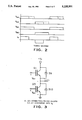
- FIG. 1 is a schematic diagram of one embodiment of an electrical converter incorporating the teachings of the present invention
- FIG. 2 is a timing diagram of various waveforms that are present in an electrical converter incorporating the teachings of the present invention
- FIG. 3 is a schematic diagram of one leg of an alternate embodiment of the invention.
- FIG. 4 is a schematic diagram of an alternate embodiment of the invention.
- FIG. 5 is a schematic diagram of another alternate embodiment of the invention.
- FIG. 6 is a schematic diagram of yet another alternate embodiment of the invention.
- FIG. 7 is a schematic diagram of still another alternate embodiment of the invention.
- FIG. 8 is a schematic diagram of still another alternate embodiment of the invention.
- This invention provides a significant reduction in the switching losses in the following manner. All explanations will be based on the half cycle during which Q1 and Q4 conduct. On a typical half cycle, Q1 and Q4 will turn on at the same time, but Q4 will turn off first (refer to FIG. 2). Thus Q2 and Q4 form the leading leg of the bridge and Q1 and Q3 form the trailing leg. When Q4 turns off, capacitors C2 and C4 decrease the rate at which the voltage across Q4 can increase. Thus Q4 turns off at almost zero voltage, and this greatly reduces its turn off loss. This process is called zero voltage switching (ZVS). After Q4 turns off, Q1 continues to conduct and C2 and C4 continue to charge.
- ZVS zero voltage switching
- I 0 is almost constant, and as long as V c4 ⁇ V 8 , I 0 continues to flow through the secondary of T1, which also holds I 0 almost constant (I 0 remains almost constant because of the large value of L 0 ).
- V c4 ⁇ V 8 I 0 will flow through D5-D7 and D6-D8 instead of the secondary.
- I 1 will now start to decrease, but V c4 will continue to charge to a value above V 8 because of the energy stored in the leakage inductance, L.sub., and I 1 will start to decrease.
- ZCS zero current switching
- V c4 may be so high as to require excessive voltage ratings for Q1-Q4.
- V c4 may be so high as to require excessive voltage ratings for Q1-Q4.
- D2 is used to prevent reverse breakdown of Q2, in which case I 1 would circulate in the Q1-Q2 loop, and some of the energy would be dissipated by Q2.
- S1, S3, D2 and D4 would be unnecessary as in FIG. 7.
- all devices in the Q1 and Q3 legs must be capable of withstanding reverse voltage avalanche. This is because Q1 and Q3 may experience forced commutation under light loading conditions, and controlled avalanche is necessary to limit the resulting voltage transients.
- This approach limits the Q1-Q4 voltage ratings, but the S2 and S4 dissipation may be significant.
- D2 and D4 prevent Q2 and Q4 breakdown and the associated heating of these devices. If Q2-Q4 breakdown is acceptable, the circuit in FIG. 1 can be used if Schottkys or Zeners are used in place of D2 and D4.
- the replacement circuit in FIG. 3 can be used if C2 and C4 discharge into V 8 is acceptable.
- V c4 also can be limited by an active clamp circuit as shown in FIG. 5.
- V c4 is limited by the circuitry associated with Q5, while V C2 is limited by the circuitry associated with Q6.
- Q5-6 can be much smaller than Q1-4.
- These circuits are similar to the common step-down switching regulator which is controlled by PWM. However, in this case the input voltage, V c4 , is regulated instead of the output, which is connected to V 8 . Assuming V c4 >V 8 , V c4 monitored by the R1-R2 attenuator and compared to the V R1 reference.
- V C4 charges to the desired regulation level
- Q5 is activated to transfer the excessive energy to C7, where it can be reused.
- This circuit avoids the losses associated with the S2 breakdown in FIG. 4, and excessive values of V C4 in FIG. 1.
- V c4 >V 8 in order to drive I to zero after Q4 turn off. Since V c4 ⁇ V 8 at smaller loads, D11 is required to keep C5 charged to V 8 and prevent excessive Q2 turn on current into C5. Note that C 5 >>C 4 .
- S1, S3, D2 and D4 can be avoided as in FIG. 7, if Q1-Q4 have adequate reverse breakdown voltages.
- the replacement circuit in FIG. 3 can be used if C2 and C4 discharge into V 8 is acceptable.
- the voltage clamp in FIG. 5 also can be used with the converter in FIG. 8 to provide an active clamp for Q1 and Q3 in addition to Q2 and Q4. This avoids the need for high voltage zener or Schottky diodes without the reverse recovery losses associated with reverse parallel diodes.
- ZCS is achieved by using breakdown diodes, such as Zeners Z2 and Z4 in parallel with Q2 and Q4. This has the advantage of avoiding the forward voltage drop of S2 and S4, but the diode breakdown voltages must be less than the reverse breakdown voltages of Q2 and Q4.
- FIG. 7 Another possibility for method 2 is shown in FIG. 7 where ZCS is achieved by simply exceeding the reverse breakdown voltage of Q2 and Q4. This avoids the use of breakdown diodes, but it has the disadvantage of increasing the dissipation in Q2 and Q4. However, this has proven to be effective for some applications. It can only be used with devices such as IGBT's or MCT's that have a large controlled reverse breakdown voltage.
- variable gap between the drive signals for Q2 and Q4 (indicated by dashed lines in FIG. 2).
- a conventional control system referred to as phase shift control, has a very small fixed gap between the Q2 and Q4 drive signals. At light load, the variable gap increases and allows additional time to charge C2 and C4 before Q2 turns on. This helps Q2 to avoid the current surge associated with turning on into a partially charged capacitor. This allows the use of larger C2 and C4 values, which further decreases the turn off losses of Q2 and Q4. Since Q1 and Q3 turn off very rapidly, the gap between their drive signals in FIG. 2 can be made extremely small. This increases the conduction time which results in better component utilization.
- the directional switching flow of current through the primary winding 14 of the transformer 16 acts as an alternating current which will induce a directional switching flow of current through a secondary winding 18 of the transformer 16 at a different voltage than the voltage of the current flow through the primary winding 14.
- the voltage in the secondary winding 18 is equal to the voltage in the primary winding 14 multiplied by the ratio of the number of turns in the secondary winding 18 to the number of turns in the primary winding 14, as is understood in the art.
- the output of the secondary winding 18 of the transformer 16 is rectified to a direct current by a rectifier bridge 20.
- the rectifier bridge has diodes D5 and D7, with a connection to the secondary winding 18 between the diodes D5 and D7, and it further has diodes D6 and D8, with a second connection to the secondary winding 18 to provide a direct current.
- This direct current is then filtered by inductor L0 and capacitor C0 before it is applied to the external load R1.
Abstract
Description
Claims (20)
Priority Applications (1)
| Application Number | Priority Date | Filing Date | Title |
|---|---|---|---|
| US07/733,168 US5235501A (en) | 1991-07-19 | 1991-07-19 | High efficiency voltage converter |
Applications Claiming Priority (1)
| Application Number | Priority Date | Filing Date | Title |
|---|---|---|---|
| US07/733,168 US5235501A (en) | 1991-07-19 | 1991-07-19 | High efficiency voltage converter |
Publications (1)
| Publication Number | Publication Date |
|---|---|
| US5235501A true US5235501A (en) | 1993-08-10 |
Family
ID=24946515
Family Applications (1)
| Application Number | Title | Priority Date | Filing Date |
|---|---|---|---|
| US07/733,168 Expired - Lifetime US5235501A (en) | 1991-07-19 | 1991-07-19 | High efficiency voltage converter |
Country Status (1)
| Country | Link |
|---|---|
| US (1) | US5235501A (en) |
Cited By (39)
| Publication number | Priority date | Publication date | Assignee | Title |
|---|---|---|---|---|
| US5402329A (en) * | 1992-12-09 | 1995-03-28 | Ernest H. Wittenbreder, Jr. | Zero voltage switching pulse width modulated power converters |
| WO1996010861A1 (en) * | 1994-09-30 | 1996-04-11 | Grinaker Electronics Limited | Ac to dc converter |
| US5532919A (en) * | 1993-03-30 | 1996-07-02 | Motorola, Inc. | Variable frequency, zero voltage switching, quasi-resonant converters with resonant bridge switch |
| US5559685A (en) * | 1994-10-12 | 1996-09-24 | Electronic Power Conditioning, Inc. | Voltage clamped parallel resonant converter with controllable duty cycle |
| US5594635A (en) * | 1993-03-30 | 1997-01-14 | Motorola, Inc. | Constant frequency, zero-voltage-switching converters with resonant switching bridge |
| US5828559A (en) * | 1997-02-03 | 1998-10-27 | Chen; Keming | Soft switching active snubber |
| EP0880220A2 (en) * | 1997-05-19 | 1998-11-25 | TRW Inc. | A phase staggered full-bridge converter with soft-PWM switching |
| US5946200A (en) * | 1995-12-02 | 1999-08-31 | Korea Electrotechnology Research Institute | Circulating current free type high frequency soft switching pulsewidth modulated full bridge DC/DC converter |
| US6259615B1 (en) | 1999-07-22 | 2001-07-10 | O2 Micro International Limited | High-efficiency adaptive DC/AC converter |
| WO2001091274A1 (en) * | 2000-05-26 | 2001-11-29 | Cleansun Pty Ltd | Power conversion system |
| US6442047B1 (en) | 1999-10-08 | 2002-08-27 | Lambda Electronics, Inc. | Power conversion apparatus and methods with reduced current and voltage switching |
| US20020180403A1 (en) * | 2001-05-24 | 2002-12-05 | Brown Fred A. | Efficient stator |
| US6501234B2 (en) | 2001-01-09 | 2002-12-31 | 02 Micro International Limited | Sequential burst mode activation circuit |
| US6531831B2 (en) | 2000-05-12 | 2003-03-11 | O2Micro International Limited | Integrated circuit for lamp heating and dimming control |
| US6570344B2 (en) | 2001-05-07 | 2003-05-27 | O2Micro International Limited | Lamp grounding and leakage current detection system |
| US20030142513A1 (en) * | 2002-01-31 | 2003-07-31 | Patrizio Vinciarelli | Factorized power architecture with point of load sine amplitude converters |
| US20030227452A1 (en) * | 2002-06-07 | 2003-12-11 | Alexandru Hartular | Adaptive LCD power supply circuit |
| US20040018142A1 (en) * | 2002-03-14 | 2004-01-29 | Marcel Tognetti | Method and arrangement for generating ultrapure steam |
| KR100436650B1 (en) * | 2002-02-28 | 2004-06-22 | 현대테크(주) | grinding machine with variable pulse power |
| US6756769B2 (en) | 2002-06-20 | 2004-06-29 | O2Micro International Limited | Enabling circuit for avoiding negative voltage transients |
| US20040178781A1 (en) * | 2003-01-22 | 2004-09-16 | Yung-Lin Lin | Controller and driving method for power circuits, electrical circuit for supplying energy and display device having the electrical circuit |
| US20040189095A1 (en) * | 2003-03-25 | 2004-09-30 | Yung-Lin Lin | Integrated power supply for an LCD panel |
| US6804129B2 (en) | 1999-07-22 | 2004-10-12 | 02 Micro International Limited | High-efficiency adaptive DC/AC converter |
| US20040207339A1 (en) * | 2003-04-15 | 2004-10-21 | Yung-Lin Lin | Power supply for an LCD panel |
| US6856519B2 (en) | 2002-05-06 | 2005-02-15 | O2Micro International Limited | Inverter controller |
| US6897698B1 (en) | 2003-05-30 | 2005-05-24 | O2Micro International Limited | Phase shifting and PWM driving circuits and methods |
| US6949912B2 (en) | 2002-06-20 | 2005-09-27 | 02Micro International Limited | Enabling circuit for avoiding negative voltage transients |
| US20050286271A1 (en) * | 2002-01-31 | 2005-12-29 | Vlt Corporation, A California Corporation | Point of load sine amplitude converters and methods |
| US20070109822A1 (en) * | 2005-11-14 | 2007-05-17 | Kan-Sheng Kuan | Zero voltage switch method for synchronous rectifier and inverter |
| US20080055951A1 (en) * | 2006-08-25 | 2008-03-06 | Semikron Elektronik Gmbh & Co. Kg | Power converter circuit and method for feeding a system from a DC voltage source |
| US7394209B2 (en) | 2004-02-11 | 2008-07-01 | 02 Micro International Limited | Liquid crystal display system with lamp feedback |
| US7515446B2 (en) | 2002-04-24 | 2009-04-07 | O2Micro International Limited | High-efficiency adaptive DC/AC converter |
| US20100246231A1 (en) * | 2009-03-31 | 2010-09-30 | TDK-Lambba Americas Inc. | Achieving zvs in a two quadrant converter using a simplified auxiliary circuit |
| CN103078506A (en) * | 2013-01-12 | 2013-05-01 | 华南理工大学 | Switching circuit for switching power supply control modes and control method for switching circuit |
| JP2013168614A (en) * | 2012-02-17 | 2013-08-29 | Mitsubishi Electric Corp | Semiconductor device and cooling system therefor |
| US20140232282A1 (en) * | 2013-02-20 | 2014-08-21 | Nxp B.V. | Resonant converter |
| US9502987B1 (en) * | 2014-02-06 | 2016-11-22 | Pai Capital Llc | Circuit and method for managing common mode noise in isolated resonant DC-DC power converters |
| JP2017017864A (en) * | 2015-07-01 | 2017-01-19 | 三菱電機株式会社 | Dc/dc converter |
| US10992235B2 (en) | 2016-10-18 | 2021-04-27 | Robert Bosch Gmbh | Soft switching full-bridge phase-shifted DC-DC converter |
Citations (6)
| Publication number | Priority date | Publication date | Assignee | Title |
|---|---|---|---|---|
| US4864483A (en) * | 1986-09-25 | 1989-09-05 | Wisconsin Alumni Research Foundation | Static power conversion method and apparatus having essentially zero switching losses and clamped voltage levels |
| US4953068A (en) * | 1989-11-08 | 1990-08-28 | Unisys Corporation | Full bridge power converter with multiple zero voltage resonant transition switching |
| US4965710A (en) * | 1989-11-16 | 1990-10-23 | International Rectifier Corporation | Insulated gate bipolar transistor power module |
| US5077651A (en) * | 1989-09-20 | 1991-12-31 | Fuji Electric Co., Ltd. | Snubber circuit of power converter |
| US5132888A (en) * | 1991-01-07 | 1992-07-21 | Unisys Corporation | Interleaved bridge converter |
| US5140510A (en) * | 1991-03-04 | 1992-08-18 | Motorola, Inc. | Constant frequency power converter |
-
1991
- 1991-07-19 US US07/733,168 patent/US5235501A/en not_active Expired - Lifetime
Patent Citations (6)
| Publication number | Priority date | Publication date | Assignee | Title |
|---|---|---|---|---|
| US4864483A (en) * | 1986-09-25 | 1989-09-05 | Wisconsin Alumni Research Foundation | Static power conversion method and apparatus having essentially zero switching losses and clamped voltage levels |
| US5077651A (en) * | 1989-09-20 | 1991-12-31 | Fuji Electric Co., Ltd. | Snubber circuit of power converter |
| US4953068A (en) * | 1989-11-08 | 1990-08-28 | Unisys Corporation | Full bridge power converter with multiple zero voltage resonant transition switching |
| US4965710A (en) * | 1989-11-16 | 1990-10-23 | International Rectifier Corporation | Insulated gate bipolar transistor power module |
| US5132888A (en) * | 1991-01-07 | 1992-07-21 | Unisys Corporation | Interleaved bridge converter |
| US5140510A (en) * | 1991-03-04 | 1992-08-18 | Motorola, Inc. | Constant frequency power converter |
Non-Patent Citations (4)
| Title |
|---|
| "A DC to DC PWM Series Resonant Converter Operated at Resonant Frequency", Vandelac et al., Aug. 1988, IEEE Transactions on Industrial Electronics, vol. 35, No. 3, p. 456. |
| "Constant Frequency Clamped-Mode Resonant Converters", Lee et al., Oct. 1988, IEEE Transactions on Industrial Electronics, vol. 3, No. 4, p. 460. |
| A DC to DC PWM Series Resonant Converter Operated at Resonant Frequency , Vandelac et al., Aug. 1988, IEEE Transactions on Industrial Electronics, vol. 35, No. 3, p. 456. * |
| Constant Frequency Clamped Mode Resonant Converters , Lee et al., Oct. 1988, IEEE Transactions on Industrial Electronics, vol. 3, No. 4, p. 460. * |
Cited By (69)
| Publication number | Priority date | Publication date | Assignee | Title |
|---|---|---|---|---|
| US5402329A (en) * | 1992-12-09 | 1995-03-28 | Ernest H. Wittenbreder, Jr. | Zero voltage switching pulse width modulated power converters |
| US5532919A (en) * | 1993-03-30 | 1996-07-02 | Motorola, Inc. | Variable frequency, zero voltage switching, quasi-resonant converters with resonant bridge switch |
| US5594635A (en) * | 1993-03-30 | 1997-01-14 | Motorola, Inc. | Constant frequency, zero-voltage-switching converters with resonant switching bridge |
| WO1996010861A1 (en) * | 1994-09-30 | 1996-04-11 | Grinaker Electronics Limited | Ac to dc converter |
| US5559685A (en) * | 1994-10-12 | 1996-09-24 | Electronic Power Conditioning, Inc. | Voltage clamped parallel resonant converter with controllable duty cycle |
| US5946200A (en) * | 1995-12-02 | 1999-08-31 | Korea Electrotechnology Research Institute | Circulating current free type high frequency soft switching pulsewidth modulated full bridge DC/DC converter |
| US5828559A (en) * | 1997-02-03 | 1998-10-27 | Chen; Keming | Soft switching active snubber |
| EP0880220A3 (en) * | 1997-05-19 | 1999-10-20 | TRW Inc. | A phase staggered full-bridge converter with soft-PWM switching |
| EP0880220A2 (en) * | 1997-05-19 | 1998-11-25 | TRW Inc. | A phase staggered full-bridge converter with soft-PWM switching |
| US7515445B2 (en) | 1999-07-22 | 2009-04-07 | 02Micro International Limited | High-efficiency adaptive DC/AC converter |
| US6259615B1 (en) | 1999-07-22 | 2001-07-10 | O2 Micro International Limited | High-efficiency adaptive DC/AC converter |
| US20050030776A1 (en) * | 1999-07-22 | 2005-02-10 | Yung-Lin Lin | High-efficiency adaptive DC/AC converter |
| US6396722B2 (en) | 1999-07-22 | 2002-05-28 | Micro International Limited | High-efficiency adaptive DC/AC converter |
| US6804129B2 (en) | 1999-07-22 | 2004-10-12 | 02 Micro International Limited | High-efficiency adaptive DC/AC converter |
| US20020180380A1 (en) * | 1999-07-22 | 2002-12-05 | Yung-Lin Lin | High-efficiency adaptive DC/AC converter |
| US7881084B2 (en) | 1999-07-22 | 2011-02-01 | O2Micro International Limited | DC/AC cold cathode fluorescent lamp inverter |
| US7417382B2 (en) | 1999-07-22 | 2008-08-26 | O2Micro International Limited | High-efficiency adaptive DC/AC converter |
| US20080246413A1 (en) * | 1999-07-22 | 2008-10-09 | O2Micro, Inc. | Dc/ac cold cathode fluorescent lamp inverter |
| US6442047B1 (en) | 1999-10-08 | 2002-08-27 | Lambda Electronics, Inc. | Power conversion apparatus and methods with reduced current and voltage switching |
| US6531831B2 (en) | 2000-05-12 | 2003-03-11 | O2Micro International Limited | Integrated circuit for lamp heating and dimming control |
| WO2001091274A1 (en) * | 2000-05-26 | 2001-11-29 | Cleansun Pty Ltd | Power conversion system |
| US7847491B2 (en) | 2001-01-09 | 2010-12-07 | O2Micro International Limited | Sequential burst mode activation circuit |
| US7477024B2 (en) | 2001-01-09 | 2009-01-13 | O2Micro International Limited | Sequential burst mode activation circuit |
| US6707264B2 (en) | 2001-01-09 | 2004-03-16 | 2Micro International Limited | Sequential burst mode activation circuit |
| US6501234B2 (en) | 2001-01-09 | 2002-12-31 | 02 Micro International Limited | Sequential burst mode activation circuit |
| US20040183469A1 (en) * | 2001-01-09 | 2004-09-23 | Yung-Lin Lin | Sequential burnst mode activation circuit |
| US6570344B2 (en) | 2001-05-07 | 2003-05-27 | O2Micro International Limited | Lamp grounding and leakage current detection system |
| US20020180403A1 (en) * | 2001-05-24 | 2002-12-05 | Brown Fred A. | Efficient stator |
| US6930893B2 (en) * | 2002-01-31 | 2005-08-16 | Vlt, Inc. | Factorized power architecture with point of load sine amplitude converters |
| US20030142513A1 (en) * | 2002-01-31 | 2003-07-31 | Patrizio Vinciarelli | Factorized power architecture with point of load sine amplitude converters |
| US7145786B2 (en) | 2002-01-31 | 2006-12-05 | Vlt, Inc. | Point of load sine amplitude converters and methods |
| US20050286271A1 (en) * | 2002-01-31 | 2005-12-29 | Vlt Corporation, A California Corporation | Point of load sine amplitude converters and methods |
| KR100436650B1 (en) * | 2002-02-28 | 2004-06-22 | 현대테크(주) | grinding machine with variable pulse power |
| US6824757B2 (en) | 2002-03-14 | 2004-11-30 | Infineon Technologies Ag | Method and arrangement for generating ultrapure steam |
| US20040018142A1 (en) * | 2002-03-14 | 2004-01-29 | Marcel Tognetti | Method and arrangement for generating ultrapure steam |
| US7515446B2 (en) | 2002-04-24 | 2009-04-07 | O2Micro International Limited | High-efficiency adaptive DC/AC converter |
| US6856519B2 (en) | 2002-05-06 | 2005-02-15 | O2Micro International Limited | Inverter controller |
| US20030227452A1 (en) * | 2002-06-07 | 2003-12-11 | Alexandru Hartular | Adaptive LCD power supply circuit |
| US6873322B2 (en) | 2002-06-07 | 2005-03-29 | 02Micro International Limited | Adaptive LCD power supply circuit |
| US6949912B2 (en) | 2002-06-20 | 2005-09-27 | 02Micro International Limited | Enabling circuit for avoiding negative voltage transients |
| US6906497B2 (en) | 2002-06-20 | 2005-06-14 | O2Micro International Limited | Enabling circuit for avoiding negative voltage transients |
| US7112943B2 (en) | 2002-06-20 | 2006-09-26 | O2Micro International Limited | Enabling circuit for avoiding negative voltage transients |
| US6756769B2 (en) | 2002-06-20 | 2004-06-29 | O2Micro International Limited | Enabling circuit for avoiding negative voltage transients |
| US7200017B2 (en) | 2003-01-22 | 2007-04-03 | O2Micro International Limited | Controller and driving method for supplying energy to display device circuitry |
| US20040178781A1 (en) * | 2003-01-22 | 2004-09-16 | Yung-Lin Lin | Controller and driving method for power circuits, electrical circuit for supplying energy and display device having the electrical circuit |
| US20040189095A1 (en) * | 2003-03-25 | 2004-09-30 | Yung-Lin Lin | Integrated power supply for an LCD panel |
| US7057611B2 (en) | 2003-03-25 | 2006-06-06 | 02Micro International Limited | Integrated power supply for an LCD panel |
| US6936975B2 (en) | 2003-04-15 | 2005-08-30 | 02Micro International Limited | Power supply for an LCD panel |
| US20040207339A1 (en) * | 2003-04-15 | 2004-10-21 | Yung-Lin Lin | Power supply for an LCD panel |
| US20060202635A1 (en) * | 2003-04-15 | 2006-09-14 | O2Micro Inc | Driving circuit for multiple cold cathode fluorescent lamps backlight applications |
| US20090039796A1 (en) * | 2003-04-15 | 2009-02-12 | Yung-Lin Lin | Power supply for an lcd display |
| US7075245B2 (en) | 2003-04-15 | 2006-07-11 | 02 Micro, Inc | Driving circuit for multiple cold cathode fluorescent lamps backlight applications |
| US7550928B2 (en) | 2003-04-15 | 2009-06-23 | O2Micro International Limited | Driving circuit for multiple cold cathode fluorescent lamps backlight applications |
| US8179053B2 (en) | 2003-04-15 | 2012-05-15 | O2Micro International Limited | Power supply for an LCD display |
| US20040263092A1 (en) * | 2003-04-15 | 2004-12-30 | Da Liu | Driving circuit for multiple cold cathode fluorescent lamps |
| US6897698B1 (en) | 2003-05-30 | 2005-05-24 | O2Micro International Limited | Phase shifting and PWM driving circuits and methods |
| US7394209B2 (en) | 2004-02-11 | 2008-07-01 | 02 Micro International Limited | Liquid crystal display system with lamp feedback |
| US20070109822A1 (en) * | 2005-11-14 | 2007-05-17 | Kan-Sheng Kuan | Zero voltage switch method for synchronous rectifier and inverter |
| US20080055951A1 (en) * | 2006-08-25 | 2008-03-06 | Semikron Elektronik Gmbh & Co. Kg | Power converter circuit and method for feeding a system from a DC voltage source |
| US7869226B2 (en) | 2009-03-31 | 2011-01-11 | Tdk-Lambda Americas Inc. | Achieving ZVS in a two quadrant converter using a simplified auxiliary circuit |
| US20100246231A1 (en) * | 2009-03-31 | 2010-09-30 | TDK-Lambba Americas Inc. | Achieving zvs in a two quadrant converter using a simplified auxiliary circuit |
| JP2013168614A (en) * | 2012-02-17 | 2013-08-29 | Mitsubishi Electric Corp | Semiconductor device and cooling system therefor |
| US9283850B2 (en) | 2012-02-17 | 2016-03-15 | Mitsubishi Electric Corporation | Semiconductor device and cooling system for semiconductor device |
| CN103078506A (en) * | 2013-01-12 | 2013-05-01 | 华南理工大学 | Switching circuit for switching power supply control modes and control method for switching circuit |
| US20140232282A1 (en) * | 2013-02-20 | 2014-08-21 | Nxp B.V. | Resonant converter |
| US9166484B2 (en) * | 2013-02-20 | 2015-10-20 | Nxp B.V. | Resonant converter |
| US9502987B1 (en) * | 2014-02-06 | 2016-11-22 | Pai Capital Llc | Circuit and method for managing common mode noise in isolated resonant DC-DC power converters |
| JP2017017864A (en) * | 2015-07-01 | 2017-01-19 | 三菱電機株式会社 | Dc/dc converter |
| US10992235B2 (en) | 2016-10-18 | 2021-04-27 | Robert Bosch Gmbh | Soft switching full-bridge phase-shifted DC-DC converter |
Similar Documents
| Publication | Publication Date | Title |
|---|---|---|
| US5235501A (en) | High efficiency voltage converter | |
| US6483724B1 (en) | DC/DC ZVS full bridge converter power supply method and apparatus | |
| KR101357070B1 (en) | High-efficiency power converter system | |
| US5132889A (en) | Resonant-transition DC-to-DC converter | |
| US3913002A (en) | Power circuits for obtaining a high power factor electronically | |
| US7272021B2 (en) | Power converter with isolated and regulated stages | |
| KR100199506B1 (en) | A zero voltage/current switching circuit for reduced ripple current of the full-bridge dc/dc converter | |
| US6172550B1 (en) | Cryogenically-cooled switching circuit | |
| US7663898B2 (en) | Switching power supply with direct conversion off AC power source | |
| US4864479A (en) | Full-bridge lossless switching converter | |
| US4706177A (en) | DC-AC inverter with overload driving capability | |
| US5923152A (en) | Power factor correction circuit with soft switched boost converter | |
| JP2677409B2 (en) | Inverter device | |
| US20070258274A1 (en) | Medium frequency power generator | |
| US5488554A (en) | Low-loss clamp circuit | |
| US6560127B2 (en) | Power conversion circuit having improved zero voltage switching | |
| US20110115446A1 (en) | System and Method for AC Voltage Regulation | |
| WO2017103648A1 (en) | Welding power supply with extended voltage characteristic | |
| US6519164B1 (en) | Single power stage AC/DC forward converter with power switch voltage clamping function | |
| US10211752B2 (en) | Direct-current power supply device and refrigeration cycle-applied apparatus | |
| Fujii et al. | Class-E rectifier using thinned-out method | |
| Vodovozov et al. | Power electronic converters | |
| EP0602495A1 (en) | Resonant-load power supply for arc welding | |
| US6343023B1 (en) | System and method for recovering energy in power converters | |
| US5229930A (en) | Welding inverter and method for controlling a welding inverter |
Legal Events
| Date | Code | Title | Description |
|---|---|---|---|
| AS | Assignment |
Owner name: UNIVERSITY OF TOLEDO, THE Free format text: ASSIGNMENT OF ASSIGNORS INTEREST.;ASSIGNORS:STUART, THOMAS A.;CHEN, KEMING;REEL/FRAME:005778/0553;SIGNING DATES FROM 19910701 TO 19910708 |
|
| STCF | Information on status: patent grant |
Free format text: PATENTED CASE |
|
| CC | Certificate of correction | ||
| FEPP | Fee payment procedure |
Free format text: PAYOR NUMBER ASSIGNED (ORIGINAL EVENT CODE: ASPN); ENTITY STATUS OF PATENT OWNER: SMALL ENTITY |
|
| FPAY | Fee payment |
Year of fee payment: 4 |
|
| FEPP | Fee payment procedure |
Free format text: PAYER NUMBER DE-ASSIGNED (ORIGINAL EVENT CODE: RMPN); ENTITY STATUS OF PATENT OWNER: SMALL ENTITY Free format text: PAYOR NUMBER ASSIGNED (ORIGINAL EVENT CODE: ASPN); ENTITY STATUS OF PATENT OWNER: SMALL ENTITY |
|
| FPAY | Fee payment |
Year of fee payment: 8 |
|
| FPAY | Fee payment |
Year of fee payment: 12 |