US5243333A - Driver for active matrix type liquid crystal display device - Google Patents
Driver for active matrix type liquid crystal display device Download PDFInfo
- Publication number
- US5243333A US5243333A US07/921,136 US92113692A US5243333A US 5243333 A US5243333 A US 5243333A US 92113692 A US92113692 A US 92113692A US 5243333 A US5243333 A US 5243333A
- Authority
- US
- United States
- Prior art keywords
- driver
- liquid crystal
- voltage
- reference voltage
- crystal display
- Prior art date
- Legal status (The legal status is an assumption and is not a legal conclusion. Google has not performed a legal analysis and makes no representation as to the accuracy of the status listed.)
- Expired - Lifetime
Links
Images


Classifications
-
- G—PHYSICS
- G09—EDUCATION; CRYPTOGRAPHY; DISPLAY; ADVERTISING; SEALS
- G09G—ARRANGEMENTS OR CIRCUITS FOR CONTROL OF INDICATING DEVICES USING STATIC MEANS TO PRESENT VARIABLE INFORMATION
- G09G3/00—Control arrangements or circuits, of interest only in connection with visual indicators other than cathode-ray tubes
- G09G3/20—Control arrangements or circuits, of interest only in connection with visual indicators other than cathode-ray tubes for presentation of an assembly of a number of characters, e.g. a page, by composing the assembly by combination of individual elements arranged in a matrix no fixed position being assigned to or needed to be assigned to the individual characters or partial characters
- G09G3/2007—Display of intermediate tones
- G09G3/2011—Display of intermediate tones by amplitude modulation
-
- G—PHYSICS
- G09—EDUCATION; CRYPTOGRAPHY; DISPLAY; ADVERTISING; SEALS
- G09G—ARRANGEMENTS OR CIRCUITS FOR CONTROL OF INDICATING DEVICES USING STATIC MEANS TO PRESENT VARIABLE INFORMATION
- G09G3/00—Control arrangements or circuits, of interest only in connection with visual indicators other than cathode-ray tubes
- G09G3/20—Control arrangements or circuits, of interest only in connection with visual indicators other than cathode-ray tubes for presentation of an assembly of a number of characters, e.g. a page, by composing the assembly by combination of individual elements arranged in a matrix no fixed position being assigned to or needed to be assigned to the individual characters or partial characters
- G09G3/34—Control arrangements or circuits, of interest only in connection with visual indicators other than cathode-ray tubes for presentation of an assembly of a number of characters, e.g. a page, by composing the assembly by combination of individual elements arranged in a matrix no fixed position being assigned to or needed to be assigned to the individual characters or partial characters by control of light from an independent source
- G09G3/36—Control arrangements or circuits, of interest only in connection with visual indicators other than cathode-ray tubes for presentation of an assembly of a number of characters, e.g. a page, by composing the assembly by combination of individual elements arranged in a matrix no fixed position being assigned to or needed to be assigned to the individual characters or partial characters by control of light from an independent source using liquid crystals
- G09G3/3611—Control of matrices with row and column drivers
- G09G3/3685—Details of drivers for data electrodes
- G09G3/3688—Details of drivers for data electrodes suitable for active matrices only
-
- G—PHYSICS
- G09—EDUCATION; CRYPTOGRAPHY; DISPLAY; ADVERTISING; SEALS
- G09G—ARRANGEMENTS OR CIRCUITS FOR CONTROL OF INDICATING DEVICES USING STATIC MEANS TO PRESENT VARIABLE INFORMATION
- G09G2310/00—Command of the display device
- G09G2310/02—Addressing, scanning or driving the display screen or processing steps related thereto
- G09G2310/0264—Details of driving circuits
- G09G2310/027—Details of drivers for data electrodes, the drivers handling digital grey scale data, e.g. use of D/A converters
-
- G—PHYSICS
- G09—EDUCATION; CRYPTOGRAPHY; DISPLAY; ADVERTISING; SEALS
- G09G—ARRANGEMENTS OR CIRCUITS FOR CONTROL OF INDICATING DEVICES USING STATIC MEANS TO PRESENT VARIABLE INFORMATION
- G09G2310/00—Command of the display device
- G09G2310/02—Addressing, scanning or driving the display screen or processing steps related thereto
- G09G2310/0264—Details of driving circuits
- G09G2310/0289—Details of voltage level shifters arranged for use in a driving circuit
-
- G—PHYSICS
- G09—EDUCATION; CRYPTOGRAPHY; DISPLAY; ADVERTISING; SEALS
- G09G—ARRANGEMENTS OR CIRCUITS FOR CONTROL OF INDICATING DEVICES USING STATIC MEANS TO PRESENT VARIABLE INFORMATION
- G09G2330/00—Aspects of power supply; Aspects of display protection and defect management
- G09G2330/02—Details of power systems and of start or stop of display operation
- G09G2330/021—Power management, e.g. power saving
Definitions
- the present invention relates to a driver for a liquid crystal display device and, more particularly, to a driver for selectively applying voltages to pixels of an active matrix type liquid crystal display device.
- an active matrix driving system As a driving system for a matrix liquid crystal display element, an active matrix driving system is widely known.
- a liquid crystal driver output circuit for a conventional multi-gradation display liquid crystal display device using, e.g., four reference voltages, a liquid crystal driver output circuit, as in FIG. 1, is used.
- Four reference voltages V R3 , V R2 , V R1 , and V R0 are respectively applied to switches SW12, SW13, SW14, and SW15 which are selectively turned on/off and constitute a first stage.
- Outputs from the adjacent pairs of switches are commonly applied to switches SW16 and SW17 which are alternatively turned on/off and constitute a second stage.
- Outputs from the switches SW16 and SW17 are commonly applied to an operational amplifier OP2 as a buffer.
- the alternatively selected reference voltage V R0 , V R1 , V R2 , or V R3 is applied from an output terminal d to a data line of an active matrix type liquid crystal display panel (not shown) and is applied to a pixel electrode in accordance with an ON/OFF operation of a thin-film transistor.
- the selective ON/OFF operations of the switches SW12 to SW17 are controlled by control signals A and B supplied in the form of digital signals.
- the control signal A has two values, e.g., 5 V and 0 V.
- the control signal A is level-shifted to an amplitude of 20 V by a level shifter LS1.
- high- or low-level outputs are obtained from output terminals Q and Q of the level shifter LS1 in accordance with the digital value of the control signal A.
- Two of the four switches SW12 to SW15 are turned on in accordance with the states of the output terminals Q and Q of the level shifter LS1.
- the control signal B is also a binary signal having values of 5 V and 0 V.
- the control signal B is level-shifted by a level shifter LS2, and outputs corresponding to its digital value are obtained from output terminals Q and Q.
- One of the switches SW16 and SW17 is turned on in accordance with the states of the output terminals Q and Q.
- one of the four reference voltages V R0 , V R1 , R R2 , and V R3 is applied to the operational amplifier OP2 as a buffer.
- an object of the present invention to provide a driver for a liquid crystal display device, in which an output voltage quickly reaches an arbitrarily selected drive reference voltage so that a stable voltage coinciding with the reference voltage can be applied to the liquid crystal display device.
- a driver for a liquid crystal display device comprising a selection circuit for selecting one of different liquid crystal drive reference voltages, an amplifier, connected between an output terminal of the selection circuit and an output terminal of the driver, for amplifying one drive reference voltage selected by the selection circuit with a gain of "1", switch means connected between the output terminal of the selection circuit and the output terminal of the driver, and control means for rendering the amplifier operative while turning off the switch means, at least in a time interval between the instant at which a selecting operation of the selection circuit is completed and the instant at which an output from the amplifier is stabilized, and rendering the amplifier inoperative while turning off the switch means, after the time interval.
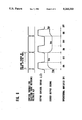
- FIG. 1 is a circuit diagram showing an output circuit of a conventional liquid crystal driver
- FIG. 2 is a circuit diagram showing a liquid crystal driver output circuit according to an embodiment of the present invention
- FIG. 3 is a circuit diagram showing an operational amplifier having an operation control function and used for the liquid crystal driver output circuit in FIG. 2;
- FIG. 4 is a circuit diagram of a level shifter used for the liquid crystal driver output circuit in FIG. 2;
- FIG. 5 is a timing chart showing input and output signals to and from the level shifter in FIG. 4;
- FIG. 6 is a timing chart showing an operation of the embodiment of the present invention.
- FIG. 2 is a circuit diagram showing an embodiment of the present invention.
- FIG. 6 is a timing chart for explaining an operation of the embodiment.
- This embodiment is a four-gradation-level liquid crystal driver which can change the brightness of each pixel in four levels by selectively using four drive reference voltages V R0 to R R3 .
- the respective drive reference voltages V R0 to V R3 are primarily selected by transfer switches SW7 to SW4, each formed by connecting a p-channel MOSFET P and an n-channel field-effect transistor N in parallel with each other. This primary selection is performed by outputs Q and Q from a level shifter LS1 which receives a control signal A for selecting drive reference voltages. As a result, the drive reference voltage R R0 or V R1 and the drive reference voltage V R2 or V R3 are selected.
- the primarily selected drive reference voltages are secondarily selected by transfer switches SW2 and SW3 which are controlled by outputs Q and Q from a level shifter LS2 to which a selection control signal B is input. As a result, one drive reference voltage is selected.
- the selected drive reference voltage is sampled/held by a capacitor C L through both an operational amplifier OP1 with an operation control terminal, whose detailed circuit diagram is shown, as an example, in FIG. 3, and a transfer switch SW1.
- Transfer switch SW1 is turned on when the operational amplifier OP1 is deactivated, and turned off when the operational amplifier OP1 is activated.
- the gain of the operational amplifier OP1 is set to be "1".
- the ON/OFF operations of the operational amplifier OP1 and the transfer switch SW1 are controlled by operation control signals Z and Z from an operation control circuit 4.
- FIG. 4 shows an arrangement of each of the known level shifters LS1 and LS2 used for the liquid crystal driver shown in FIG. 2.
- the level shifter LS1 Since the level shifters LS1 and LS2 have the same circuit arrangement, the level shifter LS1 will be described below as a representative.
- a pair of C-MOSFETs 1 and 2 and an inverter 3 are connected to each other in the manner shown in FIG. 4, and contact points C 1 and C 2 between the p-channel FETs and n-channel FETs of the C-MOSFETs 1 and 2 are respectively connected to the gates of the p-channel FETs of the C-MOSFETs located on the opposite sides.
- Control signals A and A are respectively applied to the n-channel FETs of the C-MOSFETs, and the outputs Q and Q are obtained from the output terminals at the contact points C 1 and C 2 .
- a power supply voltage V CC applied to the inverter 3 is set to be, e.g., 5 V
- a power supply voltage V DD applied to the level shifter LS1 is set to be, e g., 20 V
- FIG. 5 shows the relationship between the control signal A supplied to the level shifter LS1 shown in FIG. 4 and the outputs Q and Q. As shown in FIG. 5, the level shifter LS1 serves to convert an amplitude GND-V CC to an amplitude GND-V DD .
- reference symbols Z and Z denote outputs from the operation control circuit 4; and IN+ and IN-, input signals respectively supplied to the non-inverting and inverting terminals of the operational amplifier OP1.
- An output signal from the operational amplifier OP1 appears at an output terminal OUT.
- the drive reference voltage V R0 is output, as an initial value, from an output terminal d, and that the drive reference voltage V R3 is to be applied to the liquid crystal display device.
- the control signals A and B are set at high level to turn on the switches SW2 and SW4.
- the operational amplifier OP1 is rendered operative by using the operation control signals Z and Z.
- the load capacitor C L is quickly charged by an amplifying operation of the operational amplifier OP1, and the voltage at the driver output terminal d quickly reaches the drive reference voltage V R3 .
- the operation control signals Z and Z are inverted to render the operational amplifier OP1 inoperative and turn on the transfer switch SW1. With this operation, the potential of the driver output terminal d is forcibly set to be equal to the selected reference voltage V R3 .
- control signals A and B are respectively set at high level and low level.
- control signals A and B are respectively set at low level and high level.
- the operational amplifier OP1 and the transfer switch SW1 are controlled by the operation control signals Z and Z in the same manner as described above.
- the load capacitor C L represented as the sum of the capacitance of the liquid crystal display device and the wiring capacitance has a capacitance of about 200 pF for, e.g., a 10-inch panel.
- the operational amplifier OP1 is designed to be driven at a sufficiently high speed by a current of about several hundred ⁇ A. In this case, even if the operational amplifier OP1 is formed on a silicon substrate, a relatively small area is occupied. In this arrangement, the transfer switches SW1 to SW7 may have relatively large ON resistances (10 k ⁇ or more).
- the load capacitor C L is driven by the operational amplifier OP1 so that the voltage which is set immediately before the switch SW1 is turned on is almost equal to the final voltage set after the switch SW1 is turned on. Consequently, the transfer switches SW1 to SW7 can be formed in small areas.
- the voltage at the driver output terminal d is exactly the same as that selected by the transfer switches SW1 to SW7, the output voltage scarcely varies. Since the operational amplifier OP1 and the transfer switches SW1 to SW7 can be made relatively small, as descried above, a driver output circuit can be formed on a silicon substrate without occupying a large area as in the prior art.
- the liquid crystal driver output circuit of the present invention since the output voltage can be quickly set to a preset drive reference voltage by an operational amplifier connected in the form of a voltage follower, the sizes of drive reference voltage selection transfer switches can be minimized.
- the driver output circuit of the present invention can be formed in an area 1/4 that of the conventional driver output circuit. The effect of this reduction in size is enhanced with an increase in the number of drive reference voltages and the number of driver outputs.
- the operational amplifier is stopped and the transfer switch for holding the output voltage is operated by operation control signals. For this reason, a reduction in current consumption can be achieved.
- the problems associated with the voltage difference between driver outputs and the difference between the drive reference voltage and the driver output voltage can be solved.
- each signal line has good wiring characteristics, no interference is caused between the switches, and variations in drive reference voltage can be eliminated.
Abstract
Description
Claims (5)
Applications Claiming Priority (2)
| Application Number | Priority Date | Filing Date | Title |
|---|---|---|---|
| JP3-187972 | 1991-07-29 | ||
| JP18797291A JP3226567B2 (en) | 1991-07-29 | 1991-07-29 | Drive circuit for liquid crystal display |
Publications (1)
| Publication Number | Publication Date |
|---|---|
| US5243333A true US5243333A (en) | 1993-09-07 |
Family
ID=16215370
Family Applications (1)
| Application Number | Title | Priority Date | Filing Date |
|---|---|---|---|
| US07/921,136 Expired - Lifetime US5243333A (en) | 1991-07-29 | 1992-07-29 | Driver for active matrix type liquid crystal display device |
Country Status (2)
| Country | Link |
|---|---|
| US (1) | US5243333A (en) |
| JP (1) | JP3226567B2 (en) |
Cited By (21)
| Publication number | Priority date | Publication date | Assignee | Title |
|---|---|---|---|---|
| US5574475A (en) * | 1993-10-18 | 1996-11-12 | Crystal Semiconductor Corporation | Signal driver circuit for liquid crystal displays |
| US5635865A (en) * | 1994-06-07 | 1997-06-03 | Samsung Electronics Co., Ltd. | Power driving circuit of a thin film transistor liquid crystal display |
| US5719591A (en) * | 1993-10-18 | 1998-02-17 | Crystal Semiconductor | Signal driver circuit for liquid crystal displays |
| US5754155A (en) * | 1995-01-31 | 1998-05-19 | Sharp Kabushiki Kaisha | Image display device |
| WO1998040873A2 (en) * | 1997-03-11 | 1998-09-17 | Silicon Image, Inc. | System and method for driving columns of an active matrix display |
| US6064364A (en) * | 1993-12-27 | 2000-05-16 | Sharp Kabushiki Kaisha | Image display scanning circuit with outputs from sequentially switched pulse signals |
| US6075524A (en) * | 1995-07-28 | 2000-06-13 | 1294339 Ontario, Inc. | Integrated analog source driver for active matrix liquid crystal display |
| US6100868A (en) * | 1997-09-15 | 2000-08-08 | Silicon Image, Inc. | High density column drivers for an active matrix display |
| US6100879A (en) * | 1996-08-27 | 2000-08-08 | Silicon Image, Inc. | System and method for controlling an active matrix display |
| EP1094440A2 (en) * | 1999-10-21 | 2001-04-25 | Seiko Epson Corporation | Voltage supplying device for capacitive loads, and semiconductor device, electro-optical device and electronic instrument using the same |
| US6331847B1 (en) * | 1998-04-13 | 2001-12-18 | Samsung Electronics Co., Ltd. | Thin-film transistor liquid crystal display devices that generate gray level voltages having reduced offset margins |
| US20020145600A1 (en) * | 1999-10-21 | 2002-10-10 | Akira Morita | Voltage supplying device, and semiconductor device, electro-optical device and electronic instrument using the same |
| US20020149554A1 (en) * | 2001-04-16 | 2002-10-17 | Toshio Miyazawa | Display device having an improved video signal drive circuit |
| US6603294B2 (en) * | 1999-10-21 | 2003-08-05 | Seiko Epson Corporation | Voltage supplying device, and semiconductor device, electro-optical device and electronic instrument using the same |
| US20050018503A1 (en) * | 2003-06-23 | 2005-01-27 | Sanyo Electric Co., Ltd. | Amplifier circuit |
| US20070018937A1 (en) * | 2005-07-21 | 2007-01-25 | Jiunn-Yau Huang | Driving device for driving an lcd monitor |
| US7321255B2 (en) | 2004-03-08 | 2008-01-22 | Seiko Epson Corporation | Voltage generating circuit, data driver and display unit |
| US7952550B2 (en) | 2005-04-01 | 2011-05-31 | Panasonic Corporation | Liquid crystal driver, liquid crystal display device, and liquid crystal driving method |
| US20130162618A1 (en) * | 2009-11-23 | 2013-06-27 | Silicon Works Co., Ltd | Output voltage stabilization circuit of display device driving circuit |
| WO2013097831A3 (en) * | 2011-12-26 | 2013-08-29 | Chen Qixing | Multi-level parallel super-high speed adc and dac using logarithmic companding law |
| US20200005715A1 (en) * | 2006-04-19 | 2020-01-02 | Ignis Innovation Inc. | Stable driving scheme for active matrix displays |
Families Citing this family (8)
| Publication number | Priority date | Publication date | Assignee | Title |
|---|---|---|---|---|
| JP3777913B2 (en) * | 1999-10-28 | 2006-05-24 | 株式会社日立製作所 | Liquid crystal driving circuit and liquid crystal display device |
| JP4757388B2 (en) * | 2001-01-15 | 2011-08-24 | 株式会社 日立ディスプレイズ | Image display device and driving method thereof |
| US7102608B2 (en) | 2002-06-21 | 2006-09-05 | Himax Technologies, Inc. | Method and related apparatus for driving pixels located in a row of an LCD panel toward the same average voltage value |
| JP3661650B2 (en) | 2002-02-08 | 2005-06-15 | セイコーエプソン株式会社 | Reference voltage generation circuit, display drive circuit, and display device |
| KR100422595B1 (en) * | 2002-04-19 | 2004-03-12 | 주식회사 하이닉스반도체 | Low power tft lcd source driver |
| JP4179194B2 (en) * | 2004-03-08 | 2008-11-12 | セイコーエプソン株式会社 | Data driver, display device, and data driver control method |
| US7158065B2 (en) * | 2005-02-04 | 2007-01-02 | Tpo Displays Corp. | Signal driving circuits |
| JP4968904B2 (en) | 2006-12-08 | 2012-07-04 | ルネサスエレクトロニクス株式会社 | Display panel driving device, display panel driving method, and display device |
Citations (5)
| Publication number | Priority date | Publication date | Assignee | Title |
|---|---|---|---|---|
| US4356483A (en) * | 1977-02-14 | 1982-10-26 | Citizen Watch Company, Limited | Matrix drive system for liquid crystal display |
| US4760287A (en) * | 1986-03-29 | 1988-07-26 | Kabushiki Kaisha Toshiba | Voltage comparator circuit |
| US4857906A (en) * | 1987-10-08 | 1989-08-15 | Tektronix, Inc. | Complex waveform multiplexer for liquid crystal displays |
| US5010338A (en) * | 1987-10-19 | 1991-04-23 | Mitsubishi Denki Kabushiki Kaisha | Comparator circuit and analog to digital converter |
| US5066945A (en) * | 1987-10-26 | 1991-11-19 | Canon Kabushiki Kaisha | Driving apparatus for an electrode matrix suitable for a liquid crystal panel |
-
1991
- 1991-07-29 JP JP18797291A patent/JP3226567B2/en not_active Expired - Lifetime
-
1992
- 1992-07-29 US US07/921,136 patent/US5243333A/en not_active Expired - Lifetime
Patent Citations (5)
| Publication number | Priority date | Publication date | Assignee | Title |
|---|---|---|---|---|
| US4356483A (en) * | 1977-02-14 | 1982-10-26 | Citizen Watch Company, Limited | Matrix drive system for liquid crystal display |
| US4760287A (en) * | 1986-03-29 | 1988-07-26 | Kabushiki Kaisha Toshiba | Voltage comparator circuit |
| US4857906A (en) * | 1987-10-08 | 1989-08-15 | Tektronix, Inc. | Complex waveform multiplexer for liquid crystal displays |
| US5010338A (en) * | 1987-10-19 | 1991-04-23 | Mitsubishi Denki Kabushiki Kaisha | Comparator circuit and analog to digital converter |
| US5066945A (en) * | 1987-10-26 | 1991-11-19 | Canon Kabushiki Kaisha | Driving apparatus for an electrode matrix suitable for a liquid crystal panel |
Cited By (35)
| Publication number | Priority date | Publication date | Assignee | Title |
|---|---|---|---|---|
| US5719591A (en) * | 1993-10-18 | 1998-02-17 | Crystal Semiconductor | Signal driver circuit for liquid crystal displays |
| US5726676A (en) * | 1993-10-18 | 1998-03-10 | Crystal Semiconductor | Signal driver circuit for liquid crystal displays |
| US5574475A (en) * | 1993-10-18 | 1996-11-12 | Crystal Semiconductor Corporation | Signal driver circuit for liquid crystal displays |
| US6064364A (en) * | 1993-12-27 | 2000-05-16 | Sharp Kabushiki Kaisha | Image display scanning circuit with outputs from sequentially switched pulse signals |
| US5635865A (en) * | 1994-06-07 | 1997-06-03 | Samsung Electronics Co., Ltd. | Power driving circuit of a thin film transistor liquid crystal display |
| US5754155A (en) * | 1995-01-31 | 1998-05-19 | Sharp Kabushiki Kaisha | Image display device |
| US6075524A (en) * | 1995-07-28 | 2000-06-13 | 1294339 Ontario, Inc. | Integrated analog source driver for active matrix liquid crystal display |
| US6100879A (en) * | 1996-08-27 | 2000-08-08 | Silicon Image, Inc. | System and method for controlling an active matrix display |
| WO1998040873A3 (en) * | 1997-03-11 | 1999-01-14 | Silicon Image Inc | System and method for driving columns of an active matrix display |
| WO1998040873A2 (en) * | 1997-03-11 | 1998-09-17 | Silicon Image, Inc. | System and method for driving columns of an active matrix display |
| US6157360A (en) * | 1997-03-11 | 2000-12-05 | Silicon Image, Inc. | System and method for driving columns of an active matrix display |
| KR100423684B1 (en) * | 1997-03-11 | 2004-03-19 | 실리콘 이미지, 인크.(델라웨어주 법인) | System and method for driving columns of an active matrix display |
| US6100868A (en) * | 1997-09-15 | 2000-08-08 | Silicon Image, Inc. | High density column drivers for an active matrix display |
| US6331847B1 (en) * | 1998-04-13 | 2001-12-18 | Samsung Electronics Co., Ltd. | Thin-film transistor liquid crystal display devices that generate gray level voltages having reduced offset margins |
| US20020145600A1 (en) * | 1999-10-21 | 2002-10-10 | Akira Morita | Voltage supplying device, and semiconductor device, electro-optical device and electronic instrument using the same |
| US6888526B2 (en) | 1999-10-21 | 2005-05-03 | Seiko Epson Corporation | Voltage supplying device, and semiconductor device, electro-optical device and electronic instrument using the same |
| EP1094440A3 (en) * | 1999-10-21 | 2002-01-02 | Seiko Epson Corporation | Voltage supplying device for capacitive loads, and semiconductor device, electro-optical device and electronic instrument using the same |
| US6366065B1 (en) | 1999-10-21 | 2002-04-02 | Seiko Epson Corporation | Voltage supplying device, and semiconductor device, electro-optical device and electronic instrument using the same |
| US6603294B2 (en) * | 1999-10-21 | 2003-08-05 | Seiko Epson Corporation | Voltage supplying device, and semiconductor device, electro-optical device and electronic instrument using the same |
| EP1094440A2 (en) * | 1999-10-21 | 2001-04-25 | Seiko Epson Corporation | Voltage supplying device for capacitive loads, and semiconductor device, electro-optical device and electronic instrument using the same |
| US7193603B2 (en) | 2001-04-16 | 2007-03-20 | Hitachi, Ltd. | Display device having an improved video signal drive circuit |
| US20050088432A1 (en) * | 2001-04-16 | 2005-04-28 | Toshio Miyazawa | Display device having an improved video signal drive circuit |
| US6839047B2 (en) * | 2001-04-16 | 2005-01-04 | Hitachi, Ltd. | Display device having an improved video signal drive circuit |
| US20020149554A1 (en) * | 2001-04-16 | 2002-10-17 | Toshio Miyazawa | Display device having an improved video signal drive circuit |
| US20050018503A1 (en) * | 2003-06-23 | 2005-01-27 | Sanyo Electric Co., Ltd. | Amplifier circuit |
| US7330171B2 (en) * | 2003-06-23 | 2008-02-12 | Sanyo Electric Co., Ltd. | Amplifier circuit |
| US7321255B2 (en) | 2004-03-08 | 2008-01-22 | Seiko Epson Corporation | Voltage generating circuit, data driver and display unit |
| US7952550B2 (en) | 2005-04-01 | 2011-05-31 | Panasonic Corporation | Liquid crystal driver, liquid crystal display device, and liquid crystal driving method |
| US20070018937A1 (en) * | 2005-07-21 | 2007-01-25 | Jiunn-Yau Huang | Driving device for driving an lcd monitor |
| US20200005715A1 (en) * | 2006-04-19 | 2020-01-02 | Ignis Innovation Inc. | Stable driving scheme for active matrix displays |
| US10650754B2 (en) * | 2006-04-19 | 2020-05-12 | Ignis Innovation Inc. | Stable driving scheme for active matrix displays |
| US20130162618A1 (en) * | 2009-11-23 | 2013-06-27 | Silicon Works Co., Ltd | Output voltage stabilization circuit of display device driving circuit |
| US9143090B2 (en) * | 2009-11-23 | 2015-09-22 | Silicon Works Co., Ltd. | Output voltage stabilization circuit of display device driving circuit |
| WO2013097831A3 (en) * | 2011-12-26 | 2013-08-29 | Chen Qixing | Multi-level parallel super-high speed adc and dac using logarithmic companding law |
| US9136852B2 (en) | 2011-12-26 | 2015-09-15 | Qixing Chen | Multi-stage parallel super-high-speed ADC and DAC of logarithmic companding law |
Also Published As
| Publication number | Publication date |
|---|---|
| JPH0535211A (en) | 1993-02-12 |
| JP3226567B2 (en) | 2001-11-05 |
Similar Documents
| Publication | Publication Date | Title |
|---|---|---|
| US5243333A (en) | Driver for active matrix type liquid crystal display device | |
| US5589847A (en) | Switched capacitor analog circuits using polysilicon thin film technology | |
| US8031188B2 (en) | Digital/analog converter circuit, level shift circuit, shift register utilizing level shift circuit, sampling latch circuit, and liquid crystal display device incorporating the same | |
| KR100297140B1 (en) | A liquid crystal display driving circuit with low power consumption and precise voltage output | |
| US5973660A (en) | Matrix liquid crystal display | |
| US6052426A (en) | Shift register using M.I.S. transistors of like polarity | |
| US5818406A (en) | Driver circuit for liquid crystal display device | |
| KR100432599B1 (en) | Video device | |
| KR100292405B1 (en) | Thin film transistor liquid crystal device source driver having function of canceling offset | |
| EP1189191A2 (en) | Charge/discharge circuit for a flat panel display driver | |
| EP0731441A2 (en) | A liquid crystal display driver with threshold voltage drift compensation | |
| US20080089003A1 (en) | Driving voltage output circuit | |
| JPH07191303A (en) | Drive circuit for liquid crystal display device | |
| US6127997A (en) | Driver for liquid crystal display apparatus with no operational amplifier | |
| EP0731442B1 (en) | Signal disturbance reduction arrangement for a liquid crystal display | |
| US6919874B1 (en) | Shift register using M.I.S. transistors and supplementary column | |
| JP2000194327A (en) | Display device | |
| US20020140660A1 (en) | Liquid crystal display apparatus having level conversion circuit | |
| US5001481A (en) | MOS transistor threshold compensation circuit | |
| US6043812A (en) | Liquid crystal drive circuit and liquid crystal display device | |
| KR100281210B1 (en) | Digital Analog Converter Implemented by Simple Switch Capacitor Array and Its Control Method | |
| JPH07235844A (en) | Output buffer circuit for analog driver ic | |
| EP0686959B1 (en) | Power driving circuit of a thin film transistor liquid crystal display | |
| JP3295953B2 (en) | Liquid crystal display drive | |
| JPH09230829A (en) | Output circuit for source driver |
Legal Events
| Date | Code | Title | Description |
|---|---|---|---|
| AS | Assignment |
Owner name: NEC CORPORATION, JAPAN Free format text: ASSIGNMENT OF ASSIGNORS INTEREST.;ASSIGNORS:SHIBA, HIROSHI;SAITO, SEI;MIYAHARA, YASUHIRO;REEL/FRAME:006214/0656 Effective date: 19920722 |
|
| REMI | Maintenance fee reminder mailed | ||
| FEPP | Fee payment procedure |
Free format text: PETITION RELATED TO MAINTENANCE FEES FILED (ORIGINAL EVENT CODE: PMFP); ENTITY STATUS OF PATENT OWNER: LARGE ENTITY |
|
| FEPP | Fee payment procedure |
Free format text: PAYOR NUMBER ASSIGNED (ORIGINAL EVENT CODE: ASPN); ENTITY STATUS OF PATENT OWNER: LARGE ENTITY |
|
| FP | Lapsed due to failure to pay maintenance fee |
Effective date: 19970910 |
|
| FPAY | Fee payment |
Year of fee payment: 4 |
|
| SULP | Surcharge for late payment | ||
| FEPP | Fee payment procedure |
Free format text: PETITION RELATED TO MAINTENANCE FEES GRANTED (ORIGINAL EVENT CODE: PMFG); ENTITY STATUS OF PATENT OWNER: LARGE ENTITY |
|
| STCF | Information on status: patent grant |
Free format text: PATENTED CASE |
|
| PRDP | Patent reinstated due to the acceptance of a late maintenance fee |
Effective date: 19990326 |
|
| FPAY | Fee payment |
Year of fee payment: 8 |
|
| AS | Assignment |
Owner name: NEC ELECTRONICS CORPORATION, JAPAN Free format text: ASSIGNMENT OF ASSIGNORS INTEREST;ASSIGNOR:NEC CORPORATION;REEL/FRAME:013758/0440 Effective date: 20021101 |
|
| FPAY | Fee payment |
Year of fee payment: 12 |
|
| AS | Assignment |
Owner name: RENESAS ELECTRONICS CORPORATION, JAPAN Free format text: CHANGE OF NAME;ASSIGNOR:NEC ELECTRONICS CORPORATION;REEL/FRAME:025148/0010 Effective date: 20100401 |