US5258094A - Method for producing multilayer printed wiring boards - Google Patents
Method for producing multilayer printed wiring boards Download PDFInfo
- Publication number
- US5258094A US5258094A US07/942,746 US94274692A US5258094A US 5258094 A US5258094 A US 5258094A US 94274692 A US94274692 A US 94274692A US 5258094 A US5258094 A US 5258094A
- Authority
- US
- United States
- Prior art keywords
- layer
- conductive layer
- conductive
- insulating resin
- layers
- Prior art date
- Legal status (The legal status is an assumption and is not a legal conclusion. Google has not performed a legal analysis and makes no representation as to the accuracy of the status listed.)
- Expired - Fee Related
Links
Images


Classifications
-
- H—ELECTRICITY
- H05—ELECTRIC TECHNIQUES NOT OTHERWISE PROVIDED FOR
- H05K—PRINTED CIRCUITS; CASINGS OR CONSTRUCTIONAL DETAILS OF ELECTRIC APPARATUS; MANUFACTURE OF ASSEMBLAGES OF ELECTRICAL COMPONENTS
- H05K3/00—Apparatus or processes for manufacturing printed circuits
- H05K3/46—Manufacturing multilayer circuits
- H05K3/4611—Manufacturing multilayer circuits by laminating two or more circuit boards
- H05K3/4614—Manufacturing multilayer circuits by laminating two or more circuit boards the electrical connections between the circuit boards being made during lamination
-
- H—ELECTRICITY
- H05—ELECTRIC TECHNIQUES NOT OTHERWISE PROVIDED FOR
- H05K—PRINTED CIRCUITS; CASINGS OR CONSTRUCTIONAL DETAILS OF ELECTRIC APPARATUS; MANUFACTURE OF ASSEMBLAGES OF ELECTRICAL COMPONENTS
- H05K2201/00—Indexing scheme relating to printed circuits covered by H05K1/00
- H05K2201/03—Conductive materials
- H05K2201/0302—Properties and characteristics in general
- H05K2201/0305—Solder used for other purposes than connections between PCB or components, e.g. for filling vias or for programmable patterns
-
- H—ELECTRICITY
- H05—ELECTRIC TECHNIQUES NOT OTHERWISE PROVIDED FOR
- H05K—PRINTED CIRCUITS; CASINGS OR CONSTRUCTIONAL DETAILS OF ELECTRIC APPARATUS; MANUFACTURE OF ASSEMBLAGES OF ELECTRICAL COMPONENTS
- H05K2201/00—Indexing scheme relating to printed circuits covered by H05K1/00
- H05K2201/09—Shape and layout
- H05K2201/09209—Shape and layout details of conductors
- H05K2201/095—Conductive through-holes or vias
- H05K2201/09509—Blind vias, i.e. vias having one side closed
- H05K2201/09527—Inverse blind vias, i.e. bottoms outwards in multilayer PCB; Blind vias in centre of PCB having opposed bottoms
-
- H—ELECTRICITY
- H05—ELECTRIC TECHNIQUES NOT OTHERWISE PROVIDED FOR
- H05K—PRINTED CIRCUITS; CASINGS OR CONSTRUCTIONAL DETAILS OF ELECTRIC APPARATUS; MANUFACTURE OF ASSEMBLAGES OF ELECTRICAL COMPONENTS
- H05K2201/00—Indexing scheme relating to printed circuits covered by H05K1/00
- H05K2201/09—Shape and layout
- H05K2201/09209—Shape and layout details of conductors
- H05K2201/095—Conductive through-holes or vias
- H05K2201/09536—Buried plated through-holes, i.e. plated through-holes formed in a core before lamination
-
- H—ELECTRICITY
- H05—ELECTRIC TECHNIQUES NOT OTHERWISE PROVIDED FOR
- H05K—PRINTED CIRCUITS; CASINGS OR CONSTRUCTIONAL DETAILS OF ELECTRIC APPARATUS; MANUFACTURE OF ASSEMBLAGES OF ELECTRICAL COMPONENTS
- H05K2203/00—Indexing scheme relating to apparatus or processes for manufacturing printed circuits covered by H05K3/00
- H05K2203/06—Lamination
- H05K2203/063—Lamination of preperforated insulating layer
-
- H—ELECTRICITY
- H05—ELECTRIC TECHNIQUES NOT OTHERWISE PROVIDED FOR
- H05K—PRINTED CIRCUITS; CASINGS OR CONSTRUCTIONAL DETAILS OF ELECTRIC APPARATUS; MANUFACTURE OF ASSEMBLAGES OF ELECTRICAL COMPONENTS
- H05K2203/00—Indexing scheme relating to apparatus or processes for manufacturing printed circuits covered by H05K3/00
- H05K2203/15—Position of the PCB during processing
- H05K2203/1572—Processing both sides of a PCB by the same process; Providing a similar arrangement of components on both sides; Making interlayer connections from two sides
-
- H—ELECTRICITY
- H05—ELECTRIC TECHNIQUES NOT OTHERWISE PROVIDED FOR
- H05K—PRINTED CIRCUITS; CASINGS OR CONSTRUCTIONAL DETAILS OF ELECTRIC APPARATUS; MANUFACTURE OF ASSEMBLAGES OF ELECTRICAL COMPONENTS
- H05K3/00—Apparatus or processes for manufacturing printed circuits
- H05K3/0011—Working of insulating substrates or insulating layers
- H05K3/0017—Etching of the substrate by chemical or physical means
- H05K3/0023—Etching of the substrate by chemical or physical means by exposure and development of a photosensitive insulating layer
-
- H—ELECTRICITY
- H05—ELECTRIC TECHNIQUES NOT OTHERWISE PROVIDED FOR
- H05K—PRINTED CIRCUITS; CASINGS OR CONSTRUCTIONAL DETAILS OF ELECTRIC APPARATUS; MANUFACTURE OF ASSEMBLAGES OF ELECTRICAL COMPONENTS
- H05K3/00—Apparatus or processes for manufacturing printed circuits
- H05K3/40—Forming printed elements for providing electric connections to or between printed circuits
- H05K3/4038—Through-connections; Vertical interconnect access [VIA] connections
-
- H—ELECTRICITY
- H05—ELECTRIC TECHNIQUES NOT OTHERWISE PROVIDED FOR
- H05K—PRINTED CIRCUITS; CASINGS OR CONSTRUCTIONAL DETAILS OF ELECTRIC APPARATUS; MANUFACTURE OF ASSEMBLAGES OF ELECTRICAL COMPONENTS
- H05K3/00—Apparatus or processes for manufacturing printed circuits
- H05K3/46—Manufacturing multilayer circuits
- H05K3/4602—Manufacturing multilayer circuits characterized by a special circuit board as base or central core whereon additional circuit layers are built or additional circuit boards are laminated
-
- H—ELECTRICITY
- H05—ELECTRIC TECHNIQUES NOT OTHERWISE PROVIDED FOR
- H05K—PRINTED CIRCUITS; CASINGS OR CONSTRUCTIONAL DETAILS OF ELECTRIC APPARATUS; MANUFACTURE OF ASSEMBLAGES OF ELECTRICAL COMPONENTS
- H05K3/00—Apparatus or processes for manufacturing printed circuits
- H05K3/46—Manufacturing multilayer circuits
- H05K3/4611—Manufacturing multilayer circuits by laminating two or more circuit boards
- H05K3/4623—Manufacturing multilayer circuits by laminating two or more circuit boards the circuit boards having internal via connections between two or more circuit layers before lamination, e.g. double-sided circuit boards
-
- H—ELECTRICITY
- H05—ELECTRIC TECHNIQUES NOT OTHERWISE PROVIDED FOR
- H05K—PRINTED CIRCUITS; CASINGS OR CONSTRUCTIONAL DETAILS OF ELECTRIC APPARATUS; MANUFACTURE OF ASSEMBLAGES OF ELECTRICAL COMPONENTS
- H05K3/00—Apparatus or processes for manufacturing printed circuits
- H05K3/46—Manufacturing multilayer circuits
- H05K3/4644—Manufacturing multilayer circuits by building the multilayer layer by layer, i.e. build-up multilayer circuits
- H05K3/4647—Manufacturing multilayer circuits by building the multilayer layer by layer, i.e. build-up multilayer circuits by applying an insulating layer around previously made via studs
-
- Y—GENERAL TAGGING OF NEW TECHNOLOGICAL DEVELOPMENTS; GENERAL TAGGING OF CROSS-SECTIONAL TECHNOLOGIES SPANNING OVER SEVERAL SECTIONS OF THE IPC; TECHNICAL SUBJECTS COVERED BY FORMER USPC CROSS-REFERENCE ART COLLECTIONS [XRACs] AND DIGESTS
- Y10—TECHNICAL SUBJECTS COVERED BY FORMER USPC
- Y10T—TECHNICAL SUBJECTS COVERED BY FORMER US CLASSIFICATION
- Y10T29/00—Metal working
- Y10T29/49—Method of mechanical manufacture
- Y10T29/49002—Electrical device making
- Y10T29/49117—Conductor or circuit manufacturing
- Y10T29/49124—On flat or curved insulated base, e.g., printed circuit, etc.
- Y10T29/49155—Manufacturing circuit on or in base
- Y10T29/49165—Manufacturing circuit on or in base by forming conductive walled aperture in base
Definitions
- the present invention relates to a method for producing a multilayer printed wiring board and more particularly to a method for producing a multilayer printed wiring board whose degree of lamination and wiring density can substantially be improved.
- a conductive layer has in general been formed on the inner walls of holes for packaging parts and through-holes (hereinafter referred to as "via holes") by plating the packaging holes and via holes.
- the conventional multilayer printed wiring board has been designed such that embedded through-holes (hereinafter referred to as “inner via holes”) are formed within a part of inner layers as the degree of lamination of the multilayer printed wiring boards has become increasingly high.
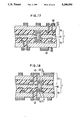
- FIGS. 1 to 8 are schematic diagrams for explaining the process for producing a multilayer printed wiring board according to the method of this prior art.
- completed multilayer printed wiring board of this type has a structure comprising six conductive layers as shown in FIG. 8 and can be produced in the following manner.
- Via holes 41 are formed through a plate 10
- Via holes 41 are formed through a plate 10 (FIG. 1A) whose upper and lower faces are laminated with copper foil layers 21 and 22 respectively (hereinafter referred to as "copper-laminated plate") and then conductive layers 61 and 62 are formed through plating as shown in FIG. 1C.
- Circuit patterns are formed on the conductive layer 62 and the copper foil layer 22 according to the known tenting method which makes use of a photosensitive dry film resist 7 as shown in FIGS. 2A and 2B.
- the via holes 41 are filled with an epoxy resin 8, followed by drying and hardening the epoxy resin to give a multilayer plate 11 for 1 ⁇ 2 layers (see FIG. 3).
- a multilayer plate 13 for 5 ⁇ 6 layers is prepared according to the same processes used above. Separately, a multilayer plate 12 for 3 ⁇ 4 layers, on which only conductive patterns are formed, is likewise prepared. Thereafter, these two multilayer plates 12 and 13 and the multilayer plate 11 for the 1 ⁇ 2 layers previously prepared are assembled through prepreg layers 51 and the resulting assembly is integrally formed by applying heat and pressure to give a multilayered board 1 shown in FIG. 4.
- Through-holes 3 for inserting parts, for electrically connecting patterns of the inner layers or for electrically connecting the upper face to the lower face are formed in the multilayered board 1 by a drill (FIG. 5) and then the assembly is plated to form a conductive layer 60 on the upper and lower faces and the inner walls of the through-holes (see FIG. 6).
- the through-holes 3 must be formed in the multilayered board 1 by a drill and then a conductive layer must be formed within the holes after the board having a multilayer structure is formed.
- the circuit patterns for a third copper foil layer 23 and a fourth copper foil layer 24 in the inner multilayer plate 12 must be designed so that the patterns do not cross the portions at which the through-holes 3 are subsequently formed and accordingly, it is not always easy to provide a multilayer printed wiring board having high wiring density.
- an object of the present invention is to provide a method for producing a multilayer printed wiring board which can eliminate the foregoing problems associated with the conventional techniques and makes it possible to provide a multilayer printed wiring board having a substantially high wiring density.
- the method for producing a multilayer printed wiring board according to the present invention comprises the steps of:
- FIGS. 1A to 1C are schematic diagrams for explaining processes of a method for producing a conventional multilayer printed wiring board
- FIGS. 2A to 2B are schematic diagrams for explaining processes, performed subsequent to the process shown in FIG. 1C, of the method for producing the conventional multilayer printed wiring board;
- FIG. 3 is a schematic diagram for explaining a process, performed subsequent to the process shown in FIG. 2B, of the method for producing the conventional multilayer printed wiring board;
- FIG. 4 is a schematic diagram for explaining a process, performed subsequent to the process shown in FIG. 3, of the method for producing the conventional multilayer printed wiring board;
- FIG. 5 is a schematic diagram for explaining a process, performed subsequent to the process shown in FIG. 4, of the method for producing the conventional multilayer printed wiring board;
- FIG. 6 is a schematic diagram for explaining a process, performed subsequent to the process shown in FIG. 5, of the method for producing the conventional multilayer printed wiring board;
- FIG. 7 is a schematic diagram for explaining a process, performed subsequent to the process shown in FIG. 6, of the method for producing the conventional multilayer printed wiring board;
- FIGS. 9A to 9C are schematic diagrams for explaining processes of a first embodiment of the method for producing a multilayer printed wiring board according to the present invention.
- FIGS. 10A to 10C are schematic diagrams for explaining processes, performed subsequent to the process shown in FIG. 9C, of the first embodiment of the method for producing a multilayer printed wiring board according to the present invention
- FIGS. 11A and 11B are schematic diagrams for explaining processes, performed subsequent to the process shown in FIG. 10C, of the first embodiment of the method for producing a multilayer printed wiring board according to the present invention
- FIGS. 12A and 12B are schematic diagrams for explaining processes, performed subsequent to the process shown in FIG. 11B, of the first embodiment of the method for producing a multilayer printed wiring board according to the present invention
- FIGS. 13A and 13B are schematic diagrams for explaining processes, performed subsequent to the process shown in FIG. 12B, of the first embodiment of the method for producing a multilayer printed wiring board according to the present invention
- FIG. 14 is a schematic diagram for explaining a process, performed subsequent to the process shown in FIG. 13B, of the first embodiment of the method for producing a multilayer printed wiring board according to the present invention
- FIG. 15 is a schematic diagram for explaining a process, performed subsequent to the process shown in FIG. 14, of the first embodiment of the method for producing a multilayer printed wiring board according to the present invention
- FIG. 16 is a schematic diagram for explaining a process, performed subsequent to the process shown in FIG. 15, of the first embodiment of the method for producing a multilayer printed wiring board according to the present invention
- FIG. 17 is a sectional view showing the structure of the completed multilayer printed wiring board of the first embodiment according to the present invention.
- FIG. 18 is a sectional view showing the structure of a completed multilayer printed wiring board of a second embodiment according to the present invention.
- FIGS. 9 to 17 show processes for producing a multilayer printed wiring board according to a first embodiment of the present invention.
- the completed multilayer printed wiring board has a structure comprising six conductive layers as shown in FIG. 17.
- a multilayer wiring board is produced as follows.
- a copper-laminated plate 10 having a thickness of from 0.1 mm to 1.6 mm and serving as a base for a multilayered board is prepared (see FIG. 9A). Copper-laminated plate 10 is provided, on both upper and lower faces, with copper foil layers 25 and 26 whose thickness ranges from 12 ⁇ m to 35 ⁇ m and on which conductive patterns for 5th and 6th layers are subsequently formed.
- Via holes 41 having a diameter ranging from 0.05 mm to 0.1 mm are formed through the copper-laminated plate 10 by a drill as shown in FIG. 9B.
- a photosensitive dry film resist 7 for instance, RISTON (trade mark) dry film TM1220 (solvent type) or TM4220 (aqueous type) available from Dupont Company (25 ⁇ m to 50 ⁇ m in thickness) according to the known tenting method, followed by development with a developer such as 1,1,1-trichloroethane (for solvent type) or sodium carbonate (for aqueous type), etching and peeling off or delaminating of the resist to form circuit patterns on the 5th conductive layer 65 and copper foil layer 25 (FIG. 10B).
- RISTON trade mark
- TM1220 solvent type
- TM4220 aqueous type
- a 4th conductive layer 64 and a lower-most conductive layer 67 of copper are formed on the entire surface of the plate including photoviaholes 42 in thickness ranging from 12 ⁇ m to 18 ⁇ m by the known electroless plating and electroplating methods to thus connect the 5th conductive layer 65 and the 4th conductive layer 64 (FIG. 12A).
- a conductive paste 5 such as eutectic solder (of 50 ⁇ m to 100 ⁇ m in thickness) is applied onto the photoviaholes 42 on the 4th conductive layer 64 through a metal mask to give a multilayered board 15 (FIG. 13B).
- the multilayered boards 14 and 15 are assembled through a prepreg layer 52 of epoxide resine or imide resine in which clearances are formed at positions corresponding to the pattern of the conductive paste 5 and then heat and pressure are applied thereto to give an integrally formed multilayered board 1 (FIG. 15).
- the conductive paste 5 is converted into a conductor and the 3rd conductive layer 63 on the multilayered board 14 is electrically connected to the 4th conductive layer 64 on the multilayered board 15.
- FIG. 18 is a sectional view showing the structure of a completed multilayer printed wiring board according to the second embodiment.
- the structure of the second embodiment is almost identical with that of the first embodiment except that conductive layers on the upper-most nd lower-most layers are electrically connected to one another through via holes 41, photoviaholes 42 and conductive paste layer 5.
- the multilayer printed wiring board of this embodiment can be produced as follows.
- Photoviaholes 42 are formed on lands 6 of via holes 41 in the similar manner used in the first embodiment to give a multilayered board 15. Then a conductive paste 5 is applied onto positions corresponding to photoviaholes 42.
- Multilayered boards 14 and 15 are assembled through a prepeg layer 52, firmly adhered to one another through application of heat and pressure and the upper-most and lower-most layers are electrically connected to complete a multilayer printed wiring board of the second embodiment.
- the present invention makes it possible to increase the degree of freedom in designing the arrangement of the circuit patterns for the inner conductive layers and accordingly multilayer printed wiring boards can be substantially improved in the degree of lamination and wiring density as compared with the conventional multilayer printed wiring boards.
Abstract
Description
Claims (6)
Applications Claiming Priority (2)
| Application Number | Priority Date | Filing Date | Title |
|---|---|---|---|
| JP3237538A JP2658661B2 (en) | 1991-09-18 | 1991-09-18 | Method for manufacturing multilayer printed wiring board |
| JP3-237538 | 1991-09-18 |
Publications (1)
| Publication Number | Publication Date |
|---|---|
| US5258094A true US5258094A (en) | 1993-11-02 |
Family
ID=17016821
Family Applications (1)
| Application Number | Title | Priority Date | Filing Date |
|---|---|---|---|
| US07/942,746 Expired - Fee Related US5258094A (en) | 1991-09-18 | 1992-09-09 | Method for producing multilayer printed wiring boards |
Country Status (2)
| Country | Link |
|---|---|
| US (1) | US5258094A (en) |
| JP (1) | JP2658661B2 (en) |
Cited By (164)
| Publication number | Priority date | Publication date | Assignee | Title |
|---|---|---|---|---|
| EP0776150A1 (en) * | 1995-06-06 | 1997-05-28 | Ibiden Co, Ltd. | Printed wiring board |
| US5841075A (en) * | 1996-11-08 | 1998-11-24 | W. L. Gore & Associates, Inc. | Method for reducing via inductance in an electronic assembly and article |
| US5867898A (en) * | 1995-04-27 | 1999-02-09 | International Business Machines Corporation | Method of manufacture multilayer circuit package |
| US5925206A (en) * | 1997-04-21 | 1999-07-20 | International Business Machines Corporation | Practical method to make blind vias in circuit boards and other substrates |
| US5937494A (en) * | 1995-09-25 | 1999-08-17 | Hewlett-Packard Company | Method for assembling an ink-jet pen having a double-sided electrical interconnect flexible circuit |
| US5976391A (en) * | 1998-01-13 | 1999-11-02 | Ford Motor Company | Continuous Flexible chemically-milled circuit assembly with multiple conductor layers and method of making same |
| US6119335A (en) * | 1997-12-02 | 2000-09-19 | Samsung Electro-Mechanics Co., Ltd. | Method for manufacturing multi-layer printed circuit board |
| US6143981A (en) * | 1998-06-24 | 2000-11-07 | Amkor Technology, Inc. | Plastic integrated circuit package and method and leadframe for making the package |
| US6175087B1 (en) | 1998-12-02 | 2001-01-16 | International Business Machines Corporation | Composite laminate circuit structure and method of forming the same |
| US6274927B1 (en) | 1999-06-03 | 2001-08-14 | Amkor Technology, Inc. | Plastic package for an optical integrated circuit device and method of making |
| US6281568B1 (en) | 1998-10-21 | 2001-08-28 | Amkor Technology, Inc. | Plastic integrated circuit device package and leadframe having partially undercut leads and die pad |
| US6320251B1 (en) | 2000-01-18 | 2001-11-20 | Amkor Technology, Inc. | Stackable package for an integrated circuit |
| US20020020907A1 (en) * | 2000-03-25 | 2002-02-21 | Amkor Technology, Inc. | Semiconductor package |
| US6404046B1 (en) | 2000-02-03 | 2002-06-11 | Amkor Technology, Inc. | Module of stacked integrated circuit packages including an interposer |
| US20020093087A1 (en) * | 2001-01-15 | 2002-07-18 | Paek Jong Sik | Semiconductor package with stacked dies |
| US20020093093A1 (en) * | 2001-01-15 | 2002-07-18 | Jong Sik Paek | Semiconductor package with stacked dies |
| US6424031B1 (en) | 2000-05-08 | 2002-07-23 | Amkor Technology, Inc. | Stackable package with heat sink |
| US6423622B1 (en) * | 1999-12-29 | 2002-07-23 | Advanced Semiconductor Engineering, Inc. | Lead-bond type chip package and manufacturing method thereof |
| US6434818B2 (en) * | 2000-03-06 | 2002-08-20 | Stanley Electric Co., Ltd. | High-frequency circuit board and method of producing the same |
| US6448633B1 (en) | 1998-11-20 | 2002-09-10 | Amkor Technology, Inc. | Semiconductor package and method of making using leadframe having lead locks to secure leads to encapsulant |
| US6476478B1 (en) | 1999-11-12 | 2002-11-05 | Amkor Technology, Inc. | Cavity semiconductor package with exposed leads and die pad |
| US20030012004A1 (en) * | 2001-07-10 | 2003-01-16 | Nippon Avionics Co., Ltd. | Printed wiring board having non-through lead mounting hole and manufacturing method of the same |
| US6518659B1 (en) | 2000-05-08 | 2003-02-11 | Amkor Technology, Inc. | Stackable package having a cavity and a lid for an electronic device |
| US6521844B1 (en) | 1999-10-29 | 2003-02-18 | International Business Machines Corporation | Through hole in a photoimageable dielectric structure with wired and uncured dielectric |
| US20030048621A1 (en) * | 2001-09-10 | 2003-03-13 | Cardiac Pacemakers, Inc. | Multi-folded printed wiring construction for an implantable medical device |
| US6605865B2 (en) | 2001-03-19 | 2003-08-12 | Amkor Technology, Inc. | Semiconductor package with optimized leadframe bonding strength |
| US6608366B1 (en) | 2002-04-15 | 2003-08-19 | Harry J. Fogelson | Lead frame with plated end leads |
| US6611047B2 (en) | 2001-10-12 | 2003-08-26 | Amkor Technology, Inc. | Semiconductor package with singulation crease |
| US6627977B1 (en) | 2002-05-09 | 2003-09-30 | Amkor Technology, Inc. | Semiconductor package including isolated ring structure |
| US6667544B1 (en) | 2000-06-30 | 2003-12-23 | Amkor Technology, Inc. | Stackable package having clips for fastening package and tool for opening clips |
| US6700187B2 (en) | 2001-03-27 | 2004-03-02 | Amkor Technology, Inc. | Semiconductor package and method for manufacturing the same |
| US20040051169A1 (en) * | 2000-02-29 | 2004-03-18 | Advanced Semiconductor Enginnering, Inc. | Lead-bond type chip package and manufacturing method thereof |
| US20040056338A1 (en) * | 1999-12-16 | 2004-03-25 | Crowley Sean Timothy | Near chip size semiconductor package |
| US6713322B2 (en) | 2001-03-27 | 2004-03-30 | Amkor Technology, Inc. | Lead frame for semiconductor package |
| US20040061217A1 (en) * | 1999-10-15 | 2004-04-01 | Ku Jae Hun | Thin and heat radiant semiconductor package and method for manufacturing |
| US6739048B2 (en) | 1998-01-08 | 2004-05-25 | International Business Machines Corporation | Process of fabricating a circuitized structure |
| US6750545B1 (en) | 2003-02-28 | 2004-06-15 | Amkor Technology, Inc. | Semiconductor package capable of die stacking |
| US6756658B1 (en) | 2001-04-06 | 2004-06-29 | Amkor Technology, Inc. | Making two lead surface mounting high power microleadframe semiconductor packages |
| US6759737B2 (en) | 2000-03-25 | 2004-07-06 | Amkor Technology, Inc. | Semiconductor package including stacked chips with aligned input/output pads |
| US20040134682A1 (en) * | 1998-09-14 | 2004-07-15 | Ibiden Co., Ltd. | Printed wiring board and its manufacturing method |
| US6777789B1 (en) | 2001-03-20 | 2004-08-17 | Amkor Technology, Inc. | Mounting for a package containing a chip |
| US6784534B1 (en) | 2002-02-06 | 2004-08-31 | Amkor Technology, Inc. | Thin integrated circuit package having an optically transparent window |
| US6790710B2 (en) | 2002-01-31 | 2004-09-14 | Asat Limited | Method of manufacturing an integrated circuit package |
| US6794740B1 (en) | 2003-03-13 | 2004-09-21 | Amkor Technology, Inc. | Leadframe package for semiconductor devices |
| US6798046B1 (en) | 2002-01-22 | 2004-09-28 | Amkor Technology, Inc. | Semiconductor package including ring structure connected to leads with vertically downset inner ends |
| US6798047B1 (en) | 2002-12-26 | 2004-09-28 | Amkor Technology, Inc. | Pre-molded leadframe |
| US6803645B2 (en) | 2000-12-29 | 2004-10-12 | Amkor Technology, Inc. | Semiconductor package including flip chip |
| US20040209399A1 (en) * | 2002-12-03 | 2004-10-21 | Shinko Electric Industries Co., Ltd. | Electronic parts packaging structure and method of manufacturing the same |
| US6818973B1 (en) | 2002-09-09 | 2004-11-16 | Amkor Technology, Inc. | Exposed lead QFP package fabricated through the use of a partial saw process |
| US20040227217A1 (en) * | 1999-10-15 | 2004-11-18 | Jang Sung Sik | Semiconductor package having improved adhesiveness and ground bonding |
| US6841414B1 (en) | 2002-06-19 | 2005-01-11 | Amkor Technology, Inc. | Saw and etch singulation method for a chip package |
| US6847103B1 (en) | 1999-11-09 | 2005-01-25 | Amkor Technology, Inc. | Semiconductor package with exposed die pad and body-locking leadframe |
| US6861720B1 (en) | 2001-08-29 | 2005-03-01 | Amkor Technology, Inc. | Placement template and method for placing optical dies |
| US6867071B1 (en) | 2002-07-12 | 2005-03-15 | Amkor Technology, Inc. | Leadframe including corner leads and semiconductor package using same |
| US20050062139A1 (en) * | 2003-09-24 | 2005-03-24 | Chung-Hsing Tzu | Reinforced die pad support structure |
| US6873041B1 (en) | 2001-11-07 | 2005-03-29 | Amkor Technology, Inc. | Power semiconductor package with strap |
| US6873032B1 (en) | 2001-04-04 | 2005-03-29 | Amkor Technology, Inc. | Thermally enhanced chip scale lead on chip semiconductor package and method of making same |
| US20050085065A1 (en) * | 2003-10-20 | 2005-04-21 | Samsung Electro-Mechanics Co., Ltd. | Parallel multi-layer printed circuit board having improved interconnection and method for manufacturing the same |
| US6885086B1 (en) | 2002-03-05 | 2005-04-26 | Amkor Technology, Inc. | Reduced copper lead frame for saw-singulated chip package |
| US6893900B1 (en) | 1998-06-24 | 2005-05-17 | Amkor Technology, Inc. | Method of making an integrated circuit package |
| US6897550B1 (en) | 2003-06-11 | 2005-05-24 | Amkor Technology, Inc. | Fully-molded leadframe stand-off feature |
| US6919620B1 (en) | 2002-09-17 | 2005-07-19 | Amkor Technology, Inc. | Compact flash memory card with clamshell leadframe |
| US6927483B1 (en) | 2003-03-07 | 2005-08-09 | Amkor Technology, Inc. | Semiconductor package exhibiting efficient lead placement |
| US6965159B1 (en) | 2001-09-19 | 2005-11-15 | Amkor Technology, Inc. | Reinforced lead-frame assembly for interconnecting circuits within a circuit module |
| US6967395B1 (en) | 2001-03-20 | 2005-11-22 | Amkor Technology, Inc. | Mounting for a package containing a chip |
| US6977431B1 (en) | 2003-11-05 | 2005-12-20 | Amkor Technology, Inc. | Stackable semiconductor package and manufacturing method thereof |
| US20060029726A1 (en) * | 2004-08-05 | 2006-02-09 | Jee-Soo Mok | Method of fabricating PCB in parallel manner |
| US7001799B1 (en) | 2003-03-13 | 2006-02-21 | Amkor Technology, Inc. | Method of making a leadframe for semiconductor devices |
| US7005326B1 (en) | 1998-06-24 | 2006-02-28 | Amkor Technology, Inc. | Method of making an integrated circuit package |
| US7009296B1 (en) | 2004-01-15 | 2006-03-07 | Amkor Technology, Inc. | Semiconductor package with substrate coupled to a peripheral side surface of a semiconductor die |
| US7008825B1 (en) | 2003-05-27 | 2006-03-07 | Amkor Technology, Inc. | Leadframe strip having enhanced testability |
| US7030474B1 (en) | 1998-06-24 | 2006-04-18 | Amkor Technology, Inc. | Plastic integrated circuit package and method and leadframe for making the package |
| US7042068B2 (en) | 2000-04-27 | 2006-05-09 | Amkor Technology, Inc. | Leadframe and semiconductor package made using the leadframe |
| US7045396B2 (en) | 1999-12-16 | 2006-05-16 | Amkor Technology, Inc. | Stackable semiconductor package and method for manufacturing same |
| US7045883B1 (en) | 2001-04-04 | 2006-05-16 | Amkor Technology, Inc. | Thermally enhanced chip scale lead on chip semiconductor package and method of making same |
| US7057268B1 (en) | 2004-01-27 | 2006-06-06 | Amkor Technology, Inc. | Cavity case with clip/plug for use on multi-media card |
| US7064009B1 (en) | 2001-04-04 | 2006-06-20 | Amkor Technology, Inc. | Thermally enhanced chip scale lead on chip semiconductor package and method of making same |
| US7071541B1 (en) | 1998-06-24 | 2006-07-04 | Amkor Technology, Inc. | Plastic integrated circuit package and method and leadframe for making the package |
| US7091594B1 (en) | 2004-01-28 | 2006-08-15 | Amkor Technology, Inc. | Leadframe type semiconductor package having reduced inductance and its manufacturing method |
| US7095103B1 (en) | 2003-05-01 | 2006-08-22 | Amkor Technology, Inc. | Leadframe based memory card |
| US7102208B1 (en) | 1999-10-15 | 2006-09-05 | Amkor Technology, Inc. | Leadframe and semiconductor package with improved solder joint strength |
| US7112474B1 (en) | 1998-06-24 | 2006-09-26 | Amkor Technology, Inc. | Method of making an integrated circuit package |
| US7115445B2 (en) | 1999-10-15 | 2006-10-03 | Amkor Technology, Inc. | Semiconductor package having reduced thickness |
| US7138707B1 (en) | 2003-10-21 | 2006-11-21 | Amkor Technology, Inc. | Semiconductor package including leads and conductive posts for providing increased functionality |
| US7144517B1 (en) | 2003-11-07 | 2006-12-05 | Amkor Technology, Inc. | Manufacturing method for leadframe and for semiconductor package using the leadframe |
| US7190062B1 (en) | 2004-06-15 | 2007-03-13 | Amkor Technology, Inc. | Embedded leadframe semiconductor package |
| US7192807B1 (en) | 2002-11-08 | 2007-03-20 | Amkor Technology, Inc. | Wafer level package and fabrication method |
| US7202554B1 (en) | 2004-08-19 | 2007-04-10 | Amkor Technology, Inc. | Semiconductor package and its manufacturing method |
| US7211879B1 (en) | 2003-11-12 | 2007-05-01 | Amkor Technology, Inc. | Semiconductor package with chamfered corners and method of manufacturing the same |
| US7217991B1 (en) | 2004-10-22 | 2007-05-15 | Amkor Technology, Inc. | Fan-in leadframe semiconductor package |
| US7245007B1 (en) | 2003-09-18 | 2007-07-17 | Amkor Technology, Inc. | Exposed lead interposer leadframe package |
| US20070176287A1 (en) * | 1999-11-05 | 2007-08-02 | Crowley Sean T | Thin integrated circuit device packages for improved radio frequency performance |
| US7253503B1 (en) | 1999-11-05 | 2007-08-07 | Amkor Technology, Inc. | Integrated circuit device packages and substrates for making the packages |
| US20070232050A1 (en) * | 2006-03-31 | 2007-10-04 | Munehiro Toyama | Embedding device in substrate cavity |
| US20080003722A1 (en) * | 2004-04-15 | 2008-01-03 | Chun David D | Transfer mold solution for molded multi-media card |
| US7332375B1 (en) | 1998-06-24 | 2008-02-19 | Amkor Technology, Inc. | Method of making an integrated circuit package |
| US7361533B1 (en) | 2002-11-08 | 2008-04-22 | Amkor Technology, Inc. | Stacked embedded leadframe |
| US20090007425A1 (en) * | 2006-02-09 | 2009-01-08 | Eiichi Shinada | Method for Manufacturing Multilayer Wiring Board |
| US20090011184A1 (en) * | 2007-07-06 | 2009-01-08 | Hon Hai Precision Industry Co., Ltd. | Method of making a flexible printed circuit board |
| US20090013525A1 (en) * | 2007-07-10 | 2009-01-15 | Samsung Electro-Mechanics Co., Ltd. | Manufacturing method for printed circuit board |
| US7485952B1 (en) | 2001-09-19 | 2009-02-03 | Amkor Technology, Inc. | Drop resistant bumpers for fully molded memory cards |
| US7507603B1 (en) | 2005-12-02 | 2009-03-24 | Amkor Technology, Inc. | Etch singulated semiconductor package |
| US7572681B1 (en) | 2005-12-08 | 2009-08-11 | Amkor Technology, Inc. | Embedded electronic component package |
| US7598598B1 (en) | 2003-02-05 | 2009-10-06 | Amkor Technology, Inc. | Offset etched corner leads for semiconductor package |
| US20090288872A1 (en) * | 2008-05-26 | 2009-11-26 | Samsung Electro-Mechanics Co., Ltd. | Printed circuit board including outmost fine circuit pattern and method of manufacturing the same |
| CN100596263C (en) * | 1998-07-23 | 2010-03-24 | 东洋钢钣株式会社 | Multilayered printed-circuit board, and method for manufacturing same |
| US7687893B2 (en) | 2006-12-27 | 2010-03-30 | Amkor Technology, Inc. | Semiconductor package having leadframe with exposed anchor pads |
| US7687899B1 (en) | 2007-08-07 | 2010-03-30 | Amkor Technology, Inc. | Dual laminate package structure with embedded elements |
| US7723210B2 (en) | 2002-11-08 | 2010-05-25 | Amkor Technology, Inc. | Direct-write wafer level chip scale package |
| US7723852B1 (en) | 2008-01-21 | 2010-05-25 | Amkor Technology, Inc. | Stacked semiconductor package and method of making same |
| US7768135B1 (en) | 2008-04-17 | 2010-08-03 | Amkor Technology, Inc. | Semiconductor package with fast power-up cycle and method of making same |
| US7777351B1 (en) | 2007-10-01 | 2010-08-17 | Amkor Technology, Inc. | Thin stacked interposer package |
| US7808084B1 (en) | 2008-05-06 | 2010-10-05 | Amkor Technology, Inc. | Semiconductor package with half-etched locking features |
| US7829990B1 (en) | 2007-01-18 | 2010-11-09 | Amkor Technology, Inc. | Stackable semiconductor package including laminate interposer |
| US7847386B1 (en) | 2007-11-05 | 2010-12-07 | Amkor Technology, Inc. | Reduced size stacked semiconductor package and method of making the same |
| US7847392B1 (en) | 2008-09-30 | 2010-12-07 | Amkor Technology, Inc. | Semiconductor device including leadframe with increased I/O |
| US7875963B1 (en) | 2008-11-21 | 2011-01-25 | Amkor Technology, Inc. | Semiconductor device including leadframe having power bars and increased I/O |
| US7902660B1 (en) | 2006-05-24 | 2011-03-08 | Amkor Technology, Inc. | Substrate for semiconductor device and manufacturing method thereof |
| US7956453B1 (en) | 2008-01-16 | 2011-06-07 | Amkor Technology, Inc. | Semiconductor package with patterning layer and method of making same |
| US7960818B1 (en) | 2009-03-04 | 2011-06-14 | Amkor Technology, Inc. | Conformal shield on punch QFN semiconductor package |
| US7968998B1 (en) | 2006-06-21 | 2011-06-28 | Amkor Technology, Inc. | Side leaded, bottom exposed pad and bottom exposed lead fusion quad flat semiconductor package |
| US7977774B2 (en) | 2007-07-10 | 2011-07-12 | Amkor Technology, Inc. | Fusion quad flat semiconductor package |
| US7982298B1 (en) | 2008-12-03 | 2011-07-19 | Amkor Technology, Inc. | Package in package semiconductor device |
| US7982297B1 (en) | 2007-03-06 | 2011-07-19 | Amkor Technology, Inc. | Stackable semiconductor package having partially exposed semiconductor die and method of fabricating the same |
| US7989933B1 (en) | 2008-10-06 | 2011-08-02 | Amkor Technology, Inc. | Increased I/O leadframe and semiconductor device including same |
| US8008758B1 (en) | 2008-10-27 | 2011-08-30 | Amkor Technology, Inc. | Semiconductor device with increased I/O leadframe |
| US8026589B1 (en) | 2009-02-23 | 2011-09-27 | Amkor Technology, Inc. | Reduced profile stackable semiconductor package |
| US8058715B1 (en) | 2009-01-09 | 2011-11-15 | Amkor Technology, Inc. | Package in package device for RF transceiver module |
| US8067821B1 (en) | 2008-04-10 | 2011-11-29 | Amkor Technology, Inc. | Flat semiconductor package with half package molding |
| US8072050B1 (en) | 2008-11-18 | 2011-12-06 | Amkor Technology, Inc. | Semiconductor device with increased I/O leadframe including passive device |
| US8089145B1 (en) | 2008-11-17 | 2012-01-03 | Amkor Technology, Inc. | Semiconductor device including increased capacity leadframe |
| US8089159B1 (en) | 2007-10-03 | 2012-01-03 | Amkor Technology, Inc. | Semiconductor package with increased I/O density and method of making the same |
| US8125064B1 (en) | 2008-07-28 | 2012-02-28 | Amkor Technology, Inc. | Increased I/O semiconductor package and method of making same |
| US8184453B1 (en) | 2008-07-31 | 2012-05-22 | Amkor Technology, Inc. | Increased capacity semiconductor package |
| US8294276B1 (en) | 2010-05-27 | 2012-10-23 | Amkor Technology, Inc. | Semiconductor device and fabricating method thereof |
| US8324511B1 (en) | 2010-04-06 | 2012-12-04 | Amkor Technology, Inc. | Through via nub reveal method and structure |
| US8390130B1 (en) | 2011-01-06 | 2013-03-05 | Amkor Technology, Inc. | Through via recessed reveal structure and method |
| US8440554B1 (en) | 2010-08-02 | 2013-05-14 | Amkor Technology, Inc. | Through via connected backside embedded circuit features structure and method |
| US8487420B1 (en) | 2008-12-08 | 2013-07-16 | Amkor Technology, Inc. | Package in package semiconductor device with film over wire |
| US8487445B1 (en) | 2010-10-05 | 2013-07-16 | Amkor Technology, Inc. | Semiconductor device having through electrodes protruding from dielectric layer |
| US8552548B1 (en) | 2011-11-29 | 2013-10-08 | Amkor Technology, Inc. | Conductive pad on protruding through electrode semiconductor device |
| US8575742B1 (en) | 2009-04-06 | 2013-11-05 | Amkor Technology, Inc. | Semiconductor device with increased I/O leadframe including power bars |
| US8648450B1 (en) | 2011-01-27 | 2014-02-11 | Amkor Technology, Inc. | Semiconductor device including leadframe with a combination of leads and lands |
| US8674485B1 (en) | 2010-12-08 | 2014-03-18 | Amkor Technology, Inc. | Semiconductor device including leadframe with downsets |
| US8680656B1 (en) | 2009-01-05 | 2014-03-25 | Amkor Technology, Inc. | Leadframe structure for concentrated photovoltaic receiver package |
| US8791501B1 (en) | 2010-12-03 | 2014-07-29 | Amkor Technology, Inc. | Integrated passive device structure and method |
| US8796561B1 (en) | 2009-10-05 | 2014-08-05 | Amkor Technology, Inc. | Fan out build up substrate stackable package and method |
| US8937381B1 (en) | 2009-12-03 | 2015-01-20 | Amkor Technology, Inc. | Thin stackable package and method |
| US20150041191A1 (en) * | 2013-08-08 | 2015-02-12 | Peking University Founder Group Co., Ltd. | Printed circuit board and preparation method thereof |
| US9048298B1 (en) | 2012-03-29 | 2015-06-02 | Amkor Technology, Inc. | Backside warpage control structure and fabrication method |
| US9129943B1 (en) | 2012-03-29 | 2015-09-08 | Amkor Technology, Inc. | Embedded component package and fabrication method |
| US9184148B2 (en) | 2013-10-24 | 2015-11-10 | Amkor Technology, Inc. | Semiconductor package and method therefor |
| US9184118B2 (en) | 2013-05-02 | 2015-11-10 | Amkor Technology Inc. | Micro lead frame structure having reinforcing portions and method |
| US20170013715A1 (en) * | 2015-07-10 | 2017-01-12 | Rohde & Schwarz Gmbh & Co. Kg | Printed circuit board and corresponding method for producing a printed circuit board |
| US9631481B1 (en) | 2011-01-27 | 2017-04-25 | Amkor Technology, Inc. | Semiconductor device including leadframe with a combination of leads and lands and method |
| US9673122B2 (en) | 2014-05-02 | 2017-06-06 | Amkor Technology, Inc. | Micro lead frame structure having reinforcing portions and method |
| US9691734B1 (en) | 2009-12-07 | 2017-06-27 | Amkor Technology, Inc. | Method of forming a plurality of electronic component packages |
| US9704725B1 (en) | 2012-03-06 | 2017-07-11 | Amkor Technology, Inc. | Semiconductor device with leadframe configured to facilitate reduced burr formation |
| CN107529292A (en) * | 2017-08-25 | 2017-12-29 | 深南电路股份有限公司 | A kind of random layer interconnection PCB preparation method |
| US10426039B2 (en) * | 2015-11-20 | 2019-09-24 | Fu Tai Hua Industry (Shenzhen) Co., Ltd. | Method for stencil printing during manufacture of printed circuit board |
| US20190297731A1 (en) * | 2016-12-15 | 2019-09-26 | Toppan Printing Co., Ltd. | Wiring board, multilayer wiring board, and method of manufacturing wiring board |
| CN111343804A (en) * | 2020-03-10 | 2020-06-26 | 景旺电子科技(龙川)有限公司 | Lamination method of multilayer thick copper metal-based circuit board |
| US10811341B2 (en) | 2009-01-05 | 2020-10-20 | Amkor Technology Singapore Holding Pte Ltd. | Semiconductor device with through-mold via |
| US11343918B2 (en) * | 2017-12-20 | 2022-05-24 | Sumitomo Electric Industries, Ltd. | Method of making printed circuit board and laminated structure |
Families Citing this family (2)
| Publication number | Priority date | Publication date | Assignee | Title |
|---|---|---|---|---|
| JP3918828B2 (en) * | 2004-05-20 | 2007-05-23 | 株式会社トッパンNecサーキットソリューションズ | Semiconductor device |
| JP4968616B2 (en) * | 2005-04-21 | 2012-07-04 | 住友電気工業株式会社 | Manufacturing method of multilayer printed wiring board |
Citations (1)
| Publication number | Priority date | Publication date | Assignee | Title |
|---|---|---|---|---|
| JPS63137499A (en) * | 1986-11-29 | 1988-06-09 | 日本電気株式会社 | Manufacture of multilayer printed interconnection board |
-
1991
- 1991-09-18 JP JP3237538A patent/JP2658661B2/en not_active Expired - Fee Related
-
1992
- 1992-09-09 US US07/942,746 patent/US5258094A/en not_active Expired - Fee Related
Patent Citations (1)
| Publication number | Priority date | Publication date | Assignee | Title |
|---|---|---|---|---|
| JPS63137499A (en) * | 1986-11-29 | 1988-06-09 | 日本電気株式会社 | Manufacture of multilayer printed interconnection board |
Cited By (290)
| Publication number | Priority date | Publication date | Assignee | Title |
|---|---|---|---|---|
| US5867898A (en) * | 1995-04-27 | 1999-02-09 | International Business Machines Corporation | Method of manufacture multilayer circuit package |
| US6291778B1 (en) | 1995-06-06 | 2001-09-18 | Ibiden, Co., Ltd. | Printed circuit boards |
| EP0776150A1 (en) * | 1995-06-06 | 1997-05-28 | Ibiden Co, Ltd. | Printed wiring board |
| EP0776150A4 (en) * | 1995-06-06 | 1999-03-31 | Ibiden Co Ltd | Printed wiring board |
| US6303880B1 (en) | 1995-06-06 | 2001-10-16 | Ibiden Co., Ltd. | Printed circuit boards |
| US5937494A (en) * | 1995-09-25 | 1999-08-17 | Hewlett-Packard Company | Method for assembling an ink-jet pen having a double-sided electrical interconnect flexible circuit |
| US6021564A (en) * | 1996-11-08 | 2000-02-08 | W. L. Gore & Associates, Inc. | Method for reducing via inductance in an electronic assembly and article |
| US5841075A (en) * | 1996-11-08 | 1998-11-24 | W. L. Gore & Associates, Inc. | Method for reducing via inductance in an electronic assembly and article |
| US5925206A (en) * | 1997-04-21 | 1999-07-20 | International Business Machines Corporation | Practical method to make blind vias in circuit boards and other substrates |
| US6119335A (en) * | 1997-12-02 | 2000-09-19 | Samsung Electro-Mechanics Co., Ltd. | Method for manufacturing multi-layer printed circuit board |
| US6739048B2 (en) | 1998-01-08 | 2004-05-25 | International Business Machines Corporation | Process of fabricating a circuitized structure |
| US5976391A (en) * | 1998-01-13 | 1999-11-02 | Ford Motor Company | Continuous Flexible chemically-milled circuit assembly with multiple conductor layers and method of making same |
| US7030474B1 (en) | 1998-06-24 | 2006-04-18 | Amkor Technology, Inc. | Plastic integrated circuit package and method and leadframe for making the package |
| US8318287B1 (en) | 1998-06-24 | 2012-11-27 | Amkor Technology, Inc. | Integrated circuit package and method of making the same |
| US7560804B1 (en) | 1998-06-24 | 2009-07-14 | Amkor Technology, Inc. | Integrated circuit package and method of making the same |
| US7112474B1 (en) | 1998-06-24 | 2006-09-26 | Amkor Technology, Inc. | Method of making an integrated circuit package |
| US7005326B1 (en) | 1998-06-24 | 2006-02-28 | Amkor Technology, Inc. | Method of making an integrated circuit package |
| US8963301B1 (en) | 1998-06-24 | 2015-02-24 | Amkor Technology, Inc. | Integrated circuit package and method of making the same |
| US6630728B2 (en) * | 1998-06-24 | 2003-10-07 | Amkor Technology, Inc. | Plastic integrated circuit package and leadframe for making the package |
| US7071541B1 (en) | 1998-06-24 | 2006-07-04 | Amkor Technology, Inc. | Plastic integrated circuit package and method and leadframe for making the package |
| US9224676B1 (en) | 1998-06-24 | 2015-12-29 | Amkor Technology, Inc. | Integrated circuit package and method of making the same |
| US6684496B2 (en) | 1998-06-24 | 2004-02-03 | Amkor Technology, Inc. | Method of making an integrated circuit package |
| US6893900B1 (en) | 1998-06-24 | 2005-05-17 | Amkor Technology, Inc. | Method of making an integrated circuit package |
| US6433277B1 (en) | 1998-06-24 | 2002-08-13 | Amkor Technology, Inc. | Plastic integrated circuit package and method and leadframe for making the package |
| US6143981A (en) * | 1998-06-24 | 2000-11-07 | Amkor Technology, Inc. | Plastic integrated circuit package and method and leadframe for making the package |
| US8853836B1 (en) | 1998-06-24 | 2014-10-07 | Amkor Technology, Inc. | Integrated circuit package and method of making the same |
| US7332375B1 (en) | 1998-06-24 | 2008-02-19 | Amkor Technology, Inc. | Method of making an integrated circuit package |
| CN100596263C (en) * | 1998-07-23 | 2010-03-24 | 东洋钢钣株式会社 | Multilayered printed-circuit board, and method for manufacturing same |
| US20040134682A1 (en) * | 1998-09-14 | 2004-07-15 | Ibiden Co., Ltd. | Printed wiring board and its manufacturing method |
| US20070266886A1 (en) * | 1998-09-14 | 2007-11-22 | Ibiden Co., Ltd. | Printed wiring board and its manufacturing method |
| US7691189B2 (en) | 1998-09-14 | 2010-04-06 | Ibiden Co., Ltd. | Printed wiring board and its manufacturing method |
| US7827680B2 (en) | 1998-09-14 | 2010-11-09 | Ibiden Co., Ltd. | Electroplating process of electroplating an elecrically conductive sustrate |
| US7230188B1 (en) * | 1998-09-14 | 2007-06-12 | Ibiden Co., Ltd. | Printed wiring board and its manufacturing method |
| US6455356B1 (en) | 1998-10-21 | 2002-09-24 | Amkor Technology | Methods for moding a leadframe in plastic integrated circuit devices |
| US6521987B1 (en) | 1998-10-21 | 2003-02-18 | Amkor Technology, Inc. | Plastic integrated circuit device package and method for making the package |
| US6281568B1 (en) | 1998-10-21 | 2001-08-28 | Amkor Technology, Inc. | Plastic integrated circuit device package and leadframe having partially undercut leads and die pad |
| US20040097016A1 (en) * | 1998-11-20 | 2004-05-20 | Yee Jae Hak | Semiconductor package and method of making leadframe having lead locks to secure leads to encapsulant |
| US7057280B2 (en) | 1998-11-20 | 2006-06-06 | Amkor Technology, Inc. | Leadframe having lead locks to secure leads to encapsulant |
| US20080036055A1 (en) * | 1998-11-20 | 2008-02-14 | Yee Jae H | Semiconductor package and method of making using leadframe having lead locks to secure leads to encapsulant |
| US20030020146A1 (en) * | 1998-11-20 | 2003-01-30 | Yee Jae Hak | Semiconductor package and method of making using leadframe having lead locks to secure leads to encapsulant |
| US6448633B1 (en) | 1998-11-20 | 2002-09-10 | Amkor Technology, Inc. | Semiconductor package and method of making using leadframe having lead locks to secure leads to encapsulant |
| US7564122B2 (en) | 1998-11-20 | 2009-07-21 | Amkor Technology, Inc. | Semiconductor package and method of making using leadframe having lead locks to secure leads to encapsulant |
| US6825062B2 (en) | 1998-11-20 | 2004-11-30 | Amkor Technology, Inc. | Semiconductor package and method of making using leadframe having lead locks to secure leads to encapsulant |
| US6451509B2 (en) | 1998-12-02 | 2002-09-17 | International Business Machines Corporation | Composite laminate circuit structure and method of forming the same |
| US6175087B1 (en) | 1998-12-02 | 2001-01-16 | International Business Machines Corporation | Composite laminate circuit structure and method of forming the same |
| US6420204B2 (en) | 1999-06-03 | 2002-07-16 | Amkor Technology, Inc. | Method of making a plastic package for an optical integrated circuit device |
| US6274927B1 (en) | 1999-06-03 | 2001-08-14 | Amkor Technology, Inc. | Plastic package for an optical integrated circuit device and method of making |
| US20040061217A1 (en) * | 1999-10-15 | 2004-04-01 | Ku Jae Hun | Thin and heat radiant semiconductor package and method for manufacturing |
| US7115445B2 (en) | 1999-10-15 | 2006-10-03 | Amkor Technology, Inc. | Semiconductor package having reduced thickness |
| US20060186517A1 (en) * | 1999-10-15 | 2006-08-24 | Jang Sung S | Semiconductor package having improved adhesiveness and ground bonding |
| US7067908B2 (en) | 1999-10-15 | 2006-06-27 | Amkor Technology, Inc. | Semiconductor package having improved adhesiveness and ground bonding |
| US7535085B2 (en) | 1999-10-15 | 2009-05-19 | Amkor Technology, Inc. | Semiconductor package having improved adhesiveness and ground bonding |
| US20040227217A1 (en) * | 1999-10-15 | 2004-11-18 | Jang Sung Sik | Semiconductor package having improved adhesiveness and ground bonding |
| US7102208B1 (en) | 1999-10-15 | 2006-09-05 | Amkor Technology, Inc. | Leadframe and semiconductor package with improved solder joint strength |
| US7321162B1 (en) | 1999-10-15 | 2008-01-22 | Amkor Technology, Inc. | Semiconductor package having reduced thickness |
| US6830875B2 (en) | 1999-10-29 | 2004-12-14 | International Business Machines Corporation | Forming a through hole in a photoimageable dielectric structure |
| US20030047357A1 (en) * | 1999-10-29 | 2003-03-13 | Fuerniss Stephen J. | Forming a through hole in a photoimageable dielectric structure |
| US6521844B1 (en) | 1999-10-29 | 2003-02-18 | International Business Machines Corporation | Through hole in a photoimageable dielectric structure with wired and uncured dielectric |
| US20070176287A1 (en) * | 1999-11-05 | 2007-08-02 | Crowley Sean T | Thin integrated circuit device packages for improved radio frequency performance |
| US7253503B1 (en) | 1999-11-05 | 2007-08-07 | Amkor Technology, Inc. | Integrated circuit device packages and substrates for making the packages |
| US6965157B1 (en) | 1999-11-09 | 2005-11-15 | Amkor Technology, Inc. | Semiconductor package with exposed die pad and body-locking leadframe |
| US6847103B1 (en) | 1999-11-09 | 2005-01-25 | Amkor Technology, Inc. | Semiconductor package with exposed die pad and body-locking leadframe |
| US6476478B1 (en) | 1999-11-12 | 2002-11-05 | Amkor Technology, Inc. | Cavity semiconductor package with exposed leads and die pad |
| US20040056338A1 (en) * | 1999-12-16 | 2004-03-25 | Crowley Sean Timothy | Near chip size semiconductor package |
| US7045396B2 (en) | 1999-12-16 | 2006-05-16 | Amkor Technology, Inc. | Stackable semiconductor package and method for manufacturing same |
| US6423622B1 (en) * | 1999-12-29 | 2002-07-23 | Advanced Semiconductor Engineering, Inc. | Lead-bond type chip package and manufacturing method thereof |
| US6642612B2 (en) | 1999-12-29 | 2003-11-04 | Advanced Semiconductor Engineering, Inc. | Lead-bond type chip package and manufacturing method thereof |
| US6320251B1 (en) | 2000-01-18 | 2001-11-20 | Amkor Technology, Inc. | Stackable package for an integrated circuit |
| US6404046B1 (en) | 2000-02-03 | 2002-06-11 | Amkor Technology, Inc. | Module of stacked integrated circuit packages including an interposer |
| US20040051169A1 (en) * | 2000-02-29 | 2004-03-18 | Advanced Semiconductor Enginnering, Inc. | Lead-bond type chip package and manufacturing method thereof |
| US7061084B2 (en) | 2000-02-29 | 2006-06-13 | Advanced Semiconductor Engineering, Inc. | Lead-bond type chip package and manufacturing method thereof |
| US6434818B2 (en) * | 2000-03-06 | 2002-08-20 | Stanley Electric Co., Ltd. | High-frequency circuit board and method of producing the same |
| US6858919B2 (en) | 2000-03-25 | 2005-02-22 | Amkor Technology, Inc. | Semiconductor package |
| US6759737B2 (en) | 2000-03-25 | 2004-07-06 | Amkor Technology, Inc. | Semiconductor package including stacked chips with aligned input/output pads |
| US20050062148A1 (en) * | 2000-03-25 | 2005-03-24 | Seo Seong Min | Semiconductor package |
| US20020020907A1 (en) * | 2000-03-25 | 2002-02-21 | Amkor Technology, Inc. | Semiconductor package |
| US6953988B2 (en) | 2000-03-25 | 2005-10-11 | Amkor Technology, Inc. | Semiconductor package |
| US8410585B2 (en) | 2000-04-27 | 2013-04-02 | Amkor Technology, Inc. | Leadframe and semiconductor package made using the leadframe |
| US9362210B2 (en) | 2000-04-27 | 2016-06-07 | Amkor Technology, Inc. | Leadframe and semiconductor package made using the leadframe |
| US7042068B2 (en) | 2000-04-27 | 2006-05-09 | Amkor Technology, Inc. | Leadframe and semiconductor package made using the leadframe |
| US20060151858A1 (en) * | 2000-04-27 | 2006-07-13 | Ahn Byung H | Leadframe and semiconductor package made using the leadframe |
| US6518659B1 (en) | 2000-05-08 | 2003-02-11 | Amkor Technology, Inc. | Stackable package having a cavity and a lid for an electronic device |
| US6424031B1 (en) | 2000-05-08 | 2002-07-23 | Amkor Technology, Inc. | Stackable package with heat sink |
| US6667544B1 (en) | 2000-06-30 | 2003-12-23 | Amkor Technology, Inc. | Stackable package having clips for fastening package and tool for opening clips |
| US20050029636A1 (en) * | 2000-12-29 | 2005-02-10 | Paek Jong Sik | Semiconductor package including flip chip |
| US6803645B2 (en) | 2000-12-29 | 2004-10-12 | Amkor Technology, Inc. | Semiconductor package including flip chip |
| US7045882B2 (en) | 2000-12-29 | 2006-05-16 | Amkor Technology, Inc. | Semiconductor package including flip chip |
| US20050156292A1 (en) * | 2001-01-15 | 2005-07-21 | Paek Jong S. | Reduced size semiconductor package with stacked dies |
| US20020093087A1 (en) * | 2001-01-15 | 2002-07-18 | Paek Jong Sik | Semiconductor package with stacked dies |
| US6927478B2 (en) | 2001-01-15 | 2005-08-09 | Amkor Technology, Inc. | Reduced size semiconductor package with stacked dies |
| US20020093093A1 (en) * | 2001-01-15 | 2002-07-18 | Jong Sik Paek | Semiconductor package with stacked dies |
| US6605865B2 (en) | 2001-03-19 | 2003-08-12 | Amkor Technology, Inc. | Semiconductor package with optimized leadframe bonding strength |
| US6777789B1 (en) | 2001-03-20 | 2004-08-17 | Amkor Technology, Inc. | Mounting for a package containing a chip |
| US6967395B1 (en) | 2001-03-20 | 2005-11-22 | Amkor Technology, Inc. | Mounting for a package containing a chip |
| US8102037B2 (en) | 2001-03-27 | 2012-01-24 | Amkor Technology, Inc. | Leadframe for semiconductor package |
| US6713322B2 (en) | 2001-03-27 | 2004-03-30 | Amkor Technology, Inc. | Lead frame for semiconductor package |
| US6700187B2 (en) | 2001-03-27 | 2004-03-02 | Amkor Technology, Inc. | Semiconductor package and method for manufacturing the same |
| US6846704B2 (en) | 2001-03-27 | 2005-01-25 | Amkor Technology, Inc. | Semiconductor package and method for manufacturing the same |
| US20060289973A1 (en) * | 2001-03-27 | 2006-12-28 | Lee Hyung J | Lead frame for semiconductor package |
| US7170150B2 (en) | 2001-03-27 | 2007-01-30 | Amkor Technology, Inc. | Lead frame for semiconductor package |
| US7521294B2 (en) | 2001-03-27 | 2009-04-21 | Amkor Technology, Inc. | Lead frame for semiconductor package |
| US7928542B2 (en) | 2001-03-27 | 2011-04-19 | Amkor Technology, Inc. | Lead frame for semiconductor package |
| US20110140250A1 (en) * | 2001-03-27 | 2011-06-16 | Hyung Ju Lee | Leadframe for semiconductor package |
| US7064009B1 (en) | 2001-04-04 | 2006-06-20 | Amkor Technology, Inc. | Thermally enhanced chip scale lead on chip semiconductor package and method of making same |
| US6873032B1 (en) | 2001-04-04 | 2005-03-29 | Amkor Technology, Inc. | Thermally enhanced chip scale lead on chip semiconductor package and method of making same |
| US7045883B1 (en) | 2001-04-04 | 2006-05-16 | Amkor Technology, Inc. | Thermally enhanced chip scale lead on chip semiconductor package and method of making same |
| US6756658B1 (en) | 2001-04-06 | 2004-06-29 | Amkor Technology, Inc. | Making two lead surface mounting high power microleadframe semiconductor packages |
| US20030012004A1 (en) * | 2001-07-10 | 2003-01-16 | Nippon Avionics Co., Ltd. | Printed wiring board having non-through lead mounting hole and manufacturing method of the same |
| US6802120B2 (en) * | 2001-07-10 | 2004-10-12 | Nippon Avionics Co., Ltd. | Method of manufacturing a printed wiring board having a non-through mounting hole |
| US6861720B1 (en) | 2001-08-29 | 2005-03-01 | Amkor Technology, Inc. | Placement template and method for placing optical dies |
| US6665191B2 (en) | 2001-09-10 | 2003-12-16 | Cardiac Pacemakers, Inc. | Multi-folded printed wiring construction for an implantable medical device |
| US20030048621A1 (en) * | 2001-09-10 | 2003-03-13 | Cardiac Pacemakers, Inc. | Multi-folded printed wiring construction for an implantable medical device |
| US6998702B1 (en) | 2001-09-19 | 2006-02-14 | Amkor Technology, Inc. | Front edge chamfer feature for fully-molded memory cards |
| US7176062B1 (en) | 2001-09-19 | 2007-02-13 | Amkor Technology, Inc. | Lead-frame method and assembly for interconnecting circuits within a circuit module |
| US7485952B1 (en) | 2001-09-19 | 2009-02-03 | Amkor Technology, Inc. | Drop resistant bumpers for fully molded memory cards |
| US6965159B1 (en) | 2001-09-19 | 2005-11-15 | Amkor Technology, Inc. | Reinforced lead-frame assembly for interconnecting circuits within a circuit module |
| US6611047B2 (en) | 2001-10-12 | 2003-08-26 | Amkor Technology, Inc. | Semiconductor package with singulation crease |
| US6873041B1 (en) | 2001-11-07 | 2005-03-29 | Amkor Technology, Inc. | Power semiconductor package with strap |
| US6798046B1 (en) | 2002-01-22 | 2004-09-28 | Amkor Technology, Inc. | Semiconductor package including ring structure connected to leads with vertically downset inner ends |
| US6790710B2 (en) | 2002-01-31 | 2004-09-14 | Asat Limited | Method of manufacturing an integrated circuit package |
| US6784534B1 (en) | 2002-02-06 | 2004-08-31 | Amkor Technology, Inc. | Thin integrated circuit package having an optically transparent window |
| US6885086B1 (en) | 2002-03-05 | 2005-04-26 | Amkor Technology, Inc. | Reduced copper lead frame for saw-singulated chip package |
| US6608366B1 (en) | 2002-04-15 | 2003-08-19 | Harry J. Fogelson | Lead frame with plated end leads |
| US6627977B1 (en) | 2002-05-09 | 2003-09-30 | Amkor Technology, Inc. | Semiconductor package including isolated ring structure |
| US6841414B1 (en) | 2002-06-19 | 2005-01-11 | Amkor Technology, Inc. | Saw and etch singulation method for a chip package |
| US6867071B1 (en) | 2002-07-12 | 2005-03-15 | Amkor Technology, Inc. | Leadframe including corner leads and semiconductor package using same |
| US6995459B2 (en) | 2002-09-09 | 2006-02-07 | Amkor Technology, Inc. | Semiconductor package with increased number of input and output pins |
| US6818973B1 (en) | 2002-09-09 | 2004-11-16 | Amkor Technology, Inc. | Exposed lead QFP package fabricated through the use of a partial saw process |
| US6876068B1 (en) | 2002-09-09 | 2005-04-05 | Amkor Technology, Inc | Semiconductor package with increased number of input and output pins |
| US7211471B1 (en) | 2002-09-09 | 2007-05-01 | Amkor Technology, Inc. | Exposed lead QFP package fabricated through the use of a partial saw process |
| US20050139969A1 (en) * | 2002-09-09 | 2005-06-30 | Lee Choon H. | Semiconductor package with increased number of input and output pins |
| US6919620B1 (en) | 2002-09-17 | 2005-07-19 | Amkor Technology, Inc. | Compact flash memory card with clamshell leadframe |
| US8710649B1 (en) | 2002-11-08 | 2014-04-29 | Amkor Technology, Inc. | Wafer level package and fabrication method |
| US9406645B1 (en) | 2002-11-08 | 2016-08-02 | Amkor Technology, Inc. | Wafer level package and fabrication method |
| US7714431B1 (en) | 2002-11-08 | 2010-05-11 | Amkor Technology, Inc. | Electronic component package comprising fan-out and fan-in traces |
| US7692286B1 (en) | 2002-11-08 | 2010-04-06 | Amkor Technology, Inc. | Two-sided fan-out wafer escape package |
| US7247523B1 (en) | 2002-11-08 | 2007-07-24 | Amkor Technology, Inc. | Two-sided wafer escape package |
| US8486764B1 (en) | 2002-11-08 | 2013-07-16 | Amkor Technology, Inc. | Wafer level package and fabrication method |
| US10665567B1 (en) | 2002-11-08 | 2020-05-26 | Amkor Technology, Inc. | Wafer level package and fabrication method |
| US8501543B1 (en) | 2002-11-08 | 2013-08-06 | Amkor Technology, Inc. | Direct-write wafer level chip scale package |
| US9871015B1 (en) | 2002-11-08 | 2018-01-16 | Amkor Technology, Inc. | Wafer level package and fabrication method |
| US8298866B1 (en) | 2002-11-08 | 2012-10-30 | Amkor Technology, Inc. | Wafer level package and fabrication method |
| US8691632B1 (en) | 2002-11-08 | 2014-04-08 | Amkor Technology, Inc. | Wafer level package and fabrication method |
| US7932595B1 (en) | 2002-11-08 | 2011-04-26 | Amkor Technology, Inc. | Electronic component package comprising fan-out traces |
| US7192807B1 (en) | 2002-11-08 | 2007-03-20 | Amkor Technology, Inc. | Wafer level package and fabrication method |
| US8188584B1 (en) | 2002-11-08 | 2012-05-29 | Amkor Technology, Inc. | Direct-write wafer level chip scale package |
| US7361533B1 (en) | 2002-11-08 | 2008-04-22 | Amkor Technology, Inc. | Stacked embedded leadframe |
| US7420272B1 (en) | 2002-11-08 | 2008-09-02 | Amkor Technology, Inc. | Two-sided wafer escape package |
| US8119455B1 (en) | 2002-11-08 | 2012-02-21 | Amkor Technology, Inc. | Wafer level package fabrication method |
| US7723210B2 (en) | 2002-11-08 | 2010-05-25 | Amkor Technology, Inc. | Direct-write wafer level chip scale package |
| US8952522B1 (en) | 2002-11-08 | 2015-02-10 | Amkor Technology, Inc. | Wafer level package and fabrication method |
| US9054117B1 (en) | 2002-11-08 | 2015-06-09 | Amkor Technology, Inc. | Wafer level package and fabrication method |
| US7084009B2 (en) * | 2002-12-03 | 2006-08-01 | Shinko Electric Industries Co., Ltd. | Method of manufacturing a packaging structure for electronic parts buried in an insulating film formed on the electronic parts and a wiring substrate |
| US20040209399A1 (en) * | 2002-12-03 | 2004-10-21 | Shinko Electric Industries Co., Ltd. | Electronic parts packaging structure and method of manufacturing the same |
| US6798047B1 (en) | 2002-12-26 | 2004-09-28 | Amkor Technology, Inc. | Pre-molded leadframe |
| US7598598B1 (en) | 2003-02-05 | 2009-10-06 | Amkor Technology, Inc. | Offset etched corner leads for semiconductor package |
| US6750545B1 (en) | 2003-02-28 | 2004-06-15 | Amkor Technology, Inc. | Semiconductor package capable of die stacking |
| US6927483B1 (en) | 2003-03-07 | 2005-08-09 | Amkor Technology, Inc. | Semiconductor package exhibiting efficient lead placement |
| US6794740B1 (en) | 2003-03-13 | 2004-09-21 | Amkor Technology, Inc. | Leadframe package for semiconductor devices |
| US7001799B1 (en) | 2003-03-13 | 2006-02-21 | Amkor Technology, Inc. | Method of making a leadframe for semiconductor devices |
| US6844615B1 (en) | 2003-03-13 | 2005-01-18 | Amkor Technology, Inc. | Leadframe package for semiconductor devices |
| US7095103B1 (en) | 2003-05-01 | 2006-08-22 | Amkor Technology, Inc. | Leadframe based memory card |
| US7008825B1 (en) | 2003-05-27 | 2006-03-07 | Amkor Technology, Inc. | Leadframe strip having enhanced testability |
| US6897550B1 (en) | 2003-06-11 | 2005-05-24 | Amkor Technology, Inc. | Fully-molded leadframe stand-off feature |
| US7245007B1 (en) | 2003-09-18 | 2007-07-17 | Amkor Technology, Inc. | Exposed lead interposer leadframe package |
| US20050062139A1 (en) * | 2003-09-24 | 2005-03-24 | Chung-Hsing Tzu | Reinforced die pad support structure |
| US7279412B2 (en) * | 2003-10-20 | 2007-10-09 | Samsung Electro-Mechanics Co., Ltd. | Parallel multi-layer printed circuit board having improved interconnection and method for manufacturing the same |
| US20050085065A1 (en) * | 2003-10-20 | 2005-04-21 | Samsung Electro-Mechanics Co., Ltd. | Parallel multi-layer printed circuit board having improved interconnection and method for manufacturing the same |
| US7138707B1 (en) | 2003-10-21 | 2006-11-21 | Amkor Technology, Inc. | Semiconductor package including leads and conductive posts for providing increased functionality |
| US6977431B1 (en) | 2003-11-05 | 2005-12-20 | Amkor Technology, Inc. | Stackable semiconductor package and manufacturing method thereof |
| US7214326B1 (en) | 2003-11-07 | 2007-05-08 | Amkor Technology, Inc. | Increased capacity leadframe and semiconductor package using the same |
| US7144517B1 (en) | 2003-11-07 | 2006-12-05 | Amkor Technology, Inc. | Manufacturing method for leadframe and for semiconductor package using the leadframe |
| US7211879B1 (en) | 2003-11-12 | 2007-05-01 | Amkor Technology, Inc. | Semiconductor package with chamfered corners and method of manufacturing the same |
| US7009296B1 (en) | 2004-01-15 | 2006-03-07 | Amkor Technology, Inc. | Semiconductor package with substrate coupled to a peripheral side surface of a semiconductor die |
| US7057268B1 (en) | 2004-01-27 | 2006-06-06 | Amkor Technology, Inc. | Cavity case with clip/plug for use on multi-media card |
| US7091594B1 (en) | 2004-01-28 | 2006-08-15 | Amkor Technology, Inc. | Leadframe type semiconductor package having reduced inductance and its manufacturing method |
| US20080003722A1 (en) * | 2004-04-15 | 2008-01-03 | Chun David D | Transfer mold solution for molded multi-media card |
| US7190062B1 (en) | 2004-06-15 | 2007-03-13 | Amkor Technology, Inc. | Embedded leadframe semiconductor package |
| US20060029726A1 (en) * | 2004-08-05 | 2006-02-09 | Jee-Soo Mok | Method of fabricating PCB in parallel manner |
| CN100463589C (en) * | 2004-08-05 | 2009-02-18 | 三星电机株式会社 | Method of fabricating PCB in parallel manner |
| US7202554B1 (en) | 2004-08-19 | 2007-04-10 | Amkor Technology, Inc. | Semiconductor package and its manufacturing method |
| US7217991B1 (en) | 2004-10-22 | 2007-05-15 | Amkor Technology, Inc. | Fan-in leadframe semiconductor package |
| US7473584B1 (en) | 2004-10-22 | 2009-01-06 | Amkor Technology, Inc. | Method for fabricating a fan-in leadframe semiconductor package |
| US7507603B1 (en) | 2005-12-02 | 2009-03-24 | Amkor Technology, Inc. | Etch singulated semiconductor package |
| US7732899B1 (en) | 2005-12-02 | 2010-06-08 | Amkor Technology, Inc. | Etch singulated semiconductor package |
| US7572681B1 (en) | 2005-12-08 | 2009-08-11 | Amkor Technology, Inc. | Embedded electronic component package |
| US7977163B1 (en) | 2005-12-08 | 2011-07-12 | Amkor Technology, Inc. | Embedded electronic component package fabrication method |
| US7870663B2 (en) | 2006-02-09 | 2011-01-18 | Hitachi Chemical Company, Ltd. | Method for manufacturing multilayer wiring board |
| CN101385403B (en) * | 2006-02-09 | 2012-08-08 | 日立化成工业株式会社 | Method for manufacturing multilayer wiring board |
| US20090007425A1 (en) * | 2006-02-09 | 2009-01-08 | Eiichi Shinada | Method for Manufacturing Multilayer Wiring Board |
| US7592202B2 (en) | 2006-03-31 | 2009-09-22 | Intel Corporation | Embedding device in substrate cavity |
| US20070232050A1 (en) * | 2006-03-31 | 2007-10-04 | Munehiro Toyama | Embedding device in substrate cavity |
| US7902660B1 (en) | 2006-05-24 | 2011-03-08 | Amkor Technology, Inc. | Substrate for semiconductor device and manufacturing method thereof |
| US7968998B1 (en) | 2006-06-21 | 2011-06-28 | Amkor Technology, Inc. | Side leaded, bottom exposed pad and bottom exposed lead fusion quad flat semiconductor package |
| US8441110B1 (en) | 2006-06-21 | 2013-05-14 | Amkor Technology, Inc. | Side leaded, bottom exposed pad and bottom exposed lead fusion quad flat semiconductor package |
| US8089141B1 (en) | 2006-12-27 | 2012-01-03 | Amkor Technology, Inc. | Semiconductor package having leadframe with exposed anchor pads |
| US7687893B2 (en) | 2006-12-27 | 2010-03-30 | Amkor Technology, Inc. | Semiconductor package having leadframe with exposed anchor pads |
| US7829990B1 (en) | 2007-01-18 | 2010-11-09 | Amkor Technology, Inc. | Stackable semiconductor package including laminate interposer |
| US7982297B1 (en) | 2007-03-06 | 2011-07-19 | Amkor Technology, Inc. | Stackable semiconductor package having partially exposed semiconductor die and method of fabricating the same |
| US7992290B2 (en) * | 2007-07-06 | 2011-08-09 | Hon Hai Precision Industry Co., Ltd. | Method of making a flexible printed circuit board |
| US20090011184A1 (en) * | 2007-07-06 | 2009-01-08 | Hon Hai Precision Industry Co., Ltd. | Method of making a flexible printed circuit board |
| US20090013525A1 (en) * | 2007-07-10 | 2009-01-15 | Samsung Electro-Mechanics Co., Ltd. | Manufacturing method for printed circuit board |
| US8304866B1 (en) | 2007-07-10 | 2012-11-06 | Amkor Technology, Inc. | Fusion quad flat semiconductor package |
| US7977774B2 (en) | 2007-07-10 | 2011-07-12 | Amkor Technology, Inc. | Fusion quad flat semiconductor package |
| US7836590B2 (en) * | 2007-07-10 | 2010-11-23 | Samsung Electro-Mechanics Co., Ltd. | Manufacturing method for printed circuit board |
| US7687899B1 (en) | 2007-08-07 | 2010-03-30 | Amkor Technology, Inc. | Dual laminate package structure with embedded elements |
| US7872343B1 (en) | 2007-08-07 | 2011-01-18 | Amkor Technology, Inc. | Dual laminate package structure with embedded elements |
| US8283767B1 (en) | 2007-08-07 | 2012-10-09 | Amkor Technology, Inc. | Dual laminate package structure with embedded elements |
| US7777351B1 (en) | 2007-10-01 | 2010-08-17 | Amkor Technology, Inc. | Thin stacked interposer package |
| US8319338B1 (en) | 2007-10-01 | 2012-11-27 | Amkor Technology, Inc. | Thin stacked interposer package |
| US8089159B1 (en) | 2007-10-03 | 2012-01-03 | Amkor Technology, Inc. | Semiconductor package with increased I/O density and method of making the same |
| US8227921B1 (en) | 2007-10-03 | 2012-07-24 | Amkor Technology, Inc. | Semiconductor package with increased I/O density and method of making same |
| US7847386B1 (en) | 2007-11-05 | 2010-12-07 | Amkor Technology, Inc. | Reduced size stacked semiconductor package and method of making the same |
| US8729710B1 (en) | 2008-01-16 | 2014-05-20 | Amkor Technology, Inc. | Semiconductor package with patterning layer and method of making same |
| US7956453B1 (en) | 2008-01-16 | 2011-06-07 | Amkor Technology, Inc. | Semiconductor package with patterning layer and method of making same |
| US7723852B1 (en) | 2008-01-21 | 2010-05-25 | Amkor Technology, Inc. | Stacked semiconductor package and method of making same |
| US7906855B1 (en) | 2008-01-21 | 2011-03-15 | Amkor Technology, Inc. | Stacked semiconductor package and method of making same |
| US8067821B1 (en) | 2008-04-10 | 2011-11-29 | Amkor Technology, Inc. | Flat semiconductor package with half package molding |
| US8084868B1 (en) | 2008-04-17 | 2011-12-27 | Amkor Technology, Inc. | Semiconductor package with fast power-up cycle and method of making same |
| US7768135B1 (en) | 2008-04-17 | 2010-08-03 | Amkor Technology, Inc. | Semiconductor package with fast power-up cycle and method of making same |
| US7808084B1 (en) | 2008-05-06 | 2010-10-05 | Amkor Technology, Inc. | Semiconductor package with half-etched locking features |
| US20090288872A1 (en) * | 2008-05-26 | 2009-11-26 | Samsung Electro-Mechanics Co., Ltd. | Printed circuit board including outmost fine circuit pattern and method of manufacturing the same |
| US20120011716A1 (en) * | 2008-05-26 | 2012-01-19 | Samsung Electro-Mechanics Co., Ltd. | Method of manufacturing printed circuit board including outmost fine circuit pattern |
| US8125064B1 (en) | 2008-07-28 | 2012-02-28 | Amkor Technology, Inc. | Increased I/O semiconductor package and method of making same |
| US8184453B1 (en) | 2008-07-31 | 2012-05-22 | Amkor Technology, Inc. | Increased capacity semiconductor package |
| US7847392B1 (en) | 2008-09-30 | 2010-12-07 | Amkor Technology, Inc. | Semiconductor device including leadframe with increased I/O |
| US8299602B1 (en) | 2008-09-30 | 2012-10-30 | Amkor Technology, Inc. | Semiconductor device including leadframe with increased I/O |
| US7989933B1 (en) | 2008-10-06 | 2011-08-02 | Amkor Technology, Inc. | Increased I/O leadframe and semiconductor device including same |
| US8432023B1 (en) | 2008-10-06 | 2013-04-30 | Amkor Technology, Inc. | Increased I/O leadframe and semiconductor device including same |
| US8823152B1 (en) | 2008-10-27 | 2014-09-02 | Amkor Technology, Inc. | Semiconductor device with increased I/O leadframe |
| US8008758B1 (en) | 2008-10-27 | 2011-08-30 | Amkor Technology, Inc. | Semiconductor device with increased I/O leadframe |
| US8089145B1 (en) | 2008-11-17 | 2012-01-03 | Amkor Technology, Inc. | Semiconductor device including increased capacity leadframe |
| US8072050B1 (en) | 2008-11-18 | 2011-12-06 | Amkor Technology, Inc. | Semiconductor device with increased I/O leadframe including passive device |
| US7875963B1 (en) | 2008-11-21 | 2011-01-25 | Amkor Technology, Inc. | Semiconductor device including leadframe having power bars and increased I/O |
| US8188579B1 (en) | 2008-11-21 | 2012-05-29 | Amkor Technology, Inc. | Semiconductor device including leadframe having power bars and increased I/O |
| US7982298B1 (en) | 2008-12-03 | 2011-07-19 | Amkor Technology, Inc. | Package in package semiconductor device |
| US8487420B1 (en) | 2008-12-08 | 2013-07-16 | Amkor Technology, Inc. | Package in package semiconductor device with film over wire |
| US8680656B1 (en) | 2009-01-05 | 2014-03-25 | Amkor Technology, Inc. | Leadframe structure for concentrated photovoltaic receiver package |
| US10811341B2 (en) | 2009-01-05 | 2020-10-20 | Amkor Technology Singapore Holding Pte Ltd. | Semiconductor device with through-mold via |
| US11869829B2 (en) | 2009-01-05 | 2024-01-09 | Amkor Technology Singapore Holding Pte. Ltd. | Semiconductor device with through-mold via |
| US8058715B1 (en) | 2009-01-09 | 2011-11-15 | Amkor Technology, Inc. | Package in package device for RF transceiver module |
| US8558365B1 (en) | 2009-01-09 | 2013-10-15 | Amkor Technology, Inc. | Package in package device for RF transceiver module |
| US8026589B1 (en) | 2009-02-23 | 2011-09-27 | Amkor Technology, Inc. | Reduced profile stackable semiconductor package |
| US7960818B1 (en) | 2009-03-04 | 2011-06-14 | Amkor Technology, Inc. | Conformal shield on punch QFN semiconductor package |
| US8729682B1 (en) | 2009-03-04 | 2014-05-20 | Amkor Technology, Inc. | Conformal shield on punch QFN semiconductor package |
| US8575742B1 (en) | 2009-04-06 | 2013-11-05 | Amkor Technology, Inc. | Semiconductor device with increased I/O leadframe including power bars |
| US8796561B1 (en) | 2009-10-05 | 2014-08-05 | Amkor Technology, Inc. | Fan out build up substrate stackable package and method |
| US8937381B1 (en) | 2009-12-03 | 2015-01-20 | Amkor Technology, Inc. | Thin stackable package and method |
| US10546833B2 (en) | 2009-12-07 | 2020-01-28 | Amkor Technology, Inc. | Method of forming a plurality of electronic component packages |
| US9691734B1 (en) | 2009-12-07 | 2017-06-27 | Amkor Technology, Inc. | Method of forming a plurality of electronic component packages |
| US9324614B1 (en) | 2010-04-06 | 2016-04-26 | Amkor Technology, Inc. | Through via nub reveal method and structure |
| US8324511B1 (en) | 2010-04-06 | 2012-12-04 | Amkor Technology, Inc. | Through via nub reveal method and structure |
| US8294276B1 (en) | 2010-05-27 | 2012-10-23 | Amkor Technology, Inc. | Semiconductor device and fabricating method thereof |
| US8440554B1 (en) | 2010-08-02 | 2013-05-14 | Amkor Technology, Inc. | Through via connected backside embedded circuit features structure and method |
| US9159672B1 (en) | 2010-08-02 | 2015-10-13 | Amkor Technology, Inc. | Through via connected backside embedded circuit features structure and method |
| US8487445B1 (en) | 2010-10-05 | 2013-07-16 | Amkor Technology, Inc. | Semiconductor device having through electrodes protruding from dielectric layer |
| US8900995B1 (en) | 2010-10-05 | 2014-12-02 | Amkor Technology, Inc. | Semiconductor device and manufacturing method thereof |
| US8791501B1 (en) | 2010-12-03 | 2014-07-29 | Amkor Technology, Inc. | Integrated passive device structure and method |
| US8674485B1 (en) | 2010-12-08 | 2014-03-18 | Amkor Technology, Inc. | Semiconductor device including leadframe with downsets |
| US9082833B1 (en) | 2011-01-06 | 2015-07-14 | Amkor Technology, Inc. | Through via recessed reveal structure and method |
| US8390130B1 (en) | 2011-01-06 | 2013-03-05 | Amkor Technology, Inc. | Through via recessed reveal structure and method |
| US8648450B1 (en) | 2011-01-27 | 2014-02-11 | Amkor Technology, Inc. | Semiconductor device including leadframe with a combination of leads and lands |
| US9275939B1 (en) | 2011-01-27 | 2016-03-01 | Amkor Technology, Inc. | Semiconductor device including leadframe with a combination of leads and lands and method |
| US9978695B1 (en) | 2011-01-27 | 2018-05-22 | Amkor Technology, Inc. | Semiconductor device including leadframe with a combination of leads and lands and method |
| US9631481B1 (en) | 2011-01-27 | 2017-04-25 | Amkor Technology, Inc. | Semiconductor device including leadframe with a combination of leads and lands and method |
| US9508631B1 (en) | 2011-01-27 | 2016-11-29 | Amkor Technology, Inc. | Semiconductor device including leadframe with a combination of leads and lands and method |
| US9947623B1 (en) | 2011-11-29 | 2018-04-17 | Amkor Technology, Inc. | Semiconductor device comprising a conductive pad on a protruding-through electrode |
| US8552548B1 (en) | 2011-11-29 | 2013-10-08 | Amkor Technology, Inc. | Conductive pad on protruding through electrode semiconductor device |
| US11043458B2 (en) | 2011-11-29 | 2021-06-22 | Amkor Technology Singapore Holding Pte. Ltd. | Method of manufacturing an electronic device comprising a conductive pad on a protruding-through electrode |
| US9431323B1 (en) | 2011-11-29 | 2016-08-30 | Amkor Technology, Inc. | Conductive pad on protruding through electrode |
| US8981572B1 (en) | 2011-11-29 | 2015-03-17 | Amkor Technology, Inc. | Conductive pad on protruding through electrode semiconductor device |
| US10410967B1 (en) | 2011-11-29 | 2019-09-10 | Amkor Technology, Inc. | Electronic device comprising a conductive pad on a protruding-through electrode |
| US10090228B1 (en) | 2012-03-06 | 2018-10-02 | Amkor Technology, Inc. | Semiconductor device with leadframe configured to facilitate reduced burr formation |
| US9704725B1 (en) | 2012-03-06 | 2017-07-11 | Amkor Technology, Inc. | Semiconductor device with leadframe configured to facilitate reduced burr formation |
| US9048298B1 (en) | 2012-03-29 | 2015-06-02 | Amkor Technology, Inc. | Backside warpage control structure and fabrication method |
| US10014240B1 (en) | 2012-03-29 | 2018-07-03 | Amkor Technology, Inc. | Embedded component package and fabrication method |
| US9129943B1 (en) | 2012-03-29 | 2015-09-08 | Amkor Technology, Inc. | Embedded component package and fabrication method |
| US9184118B2 (en) | 2013-05-02 | 2015-11-10 | Amkor Technology Inc. | Micro lead frame structure having reinforcing portions and method |
| US20150041191A1 (en) * | 2013-08-08 | 2015-02-12 | Peking University Founder Group Co., Ltd. | Printed circuit board and preparation method thereof |
| US9184148B2 (en) | 2013-10-24 | 2015-11-10 | Amkor Technology, Inc. | Semiconductor package and method therefor |
| US9543235B2 (en) | 2013-10-24 | 2017-01-10 | Amkor Technology, Inc. | Semiconductor package and method therefor |
| US9673122B2 (en) | 2014-05-02 | 2017-06-06 | Amkor Technology, Inc. | Micro lead frame structure having reinforcing portions and method |
| US10433432B2 (en) | 2015-07-10 | 2019-10-01 | Rohde & Schwarz Gmbh & Co. Kg | Printed circuit board and corresponding method for producing a printed circuit board |
| US20170013715A1 (en) * | 2015-07-10 | 2017-01-12 | Rohde & Schwarz Gmbh & Co. Kg | Printed circuit board and corresponding method for producing a printed circuit board |
| US10426039B2 (en) * | 2015-11-20 | 2019-09-24 | Fu Tai Hua Industry (Shenzhen) Co., Ltd. | Method for stencil printing during manufacture of printed circuit board |
| US10966324B2 (en) * | 2016-12-15 | 2021-03-30 | Toppan Printing Co., Ltd. | Wiring board, multilayer wiring board, and method of manufacturing wiring board |
| US20190297731A1 (en) * | 2016-12-15 | 2019-09-26 | Toppan Printing Co., Ltd. | Wiring board, multilayer wiring board, and method of manufacturing wiring board |
| CN107529292A (en) * | 2017-08-25 | 2017-12-29 | 深南电路股份有限公司 | A kind of random layer interconnection PCB preparation method |
| US11343918B2 (en) * | 2017-12-20 | 2022-05-24 | Sumitomo Electric Industries, Ltd. | Method of making printed circuit board and laminated structure |
| CN111343804A (en) * | 2020-03-10 | 2020-06-26 | 景旺电子科技(龙川)有限公司 | Lamination method of multilayer thick copper metal-based circuit board |
Also Published As
| Publication number | Publication date |
|---|---|
| JP2658661B2 (en) | 1997-09-30 |
| JPH0575269A (en) | 1993-03-26 |
Similar Documents
| Publication | Publication Date | Title |
|---|---|---|
| US5258094A (en) | Method for producing multilayer printed wiring boards | |
| KR100345530B1 (en) | Two signal one power plane circuit board | |
| US7353590B2 (en) | Method of forming printed circuit card | |
| JP3232292B2 (en) | Method for forming chip carrier and circuit board | |
| JPH0710029B2 (en) | Method for manufacturing laminated circuit board | |
| KR20040061410A (en) | PCB with the plated through holes filled with copper with copper and the fabricating method thereof | |
| JP4395959B2 (en) | Method for manufacturing printed wiring board | |
| JP3817291B2 (en) | Printed wiring board | |
| JP3713726B2 (en) | Multilayer printed wiring board | |
| JP4059386B2 (en) | Multilayer printed wiring board and manufacturing method thereof | |
| JP2622848B2 (en) | Manufacturing method of printed wiring board | |
| JPH06252529A (en) | Manufacture of printed wiring board | |
| JP2647007B2 (en) | Manufacturing method of printed wiring board | |
| JPH09326561A (en) | Multilayer printed wiring board and manufacture thereof | |
| JPS5921095A (en) | Method of producing multilayer printed circuit board | |
| JP3648753B2 (en) | Wiring board manufacturing method | |
| JPH077264A (en) | Manufacture of printed wiring board | |
| JPH02119298A (en) | Manufacture of multilayer printed wiring board for mounting semiconductor element | |
| JP4337408B2 (en) | Method for manufacturing printed wiring board | |
| KR20230152433A (en) | Method of manufacturing printed circuit board with fine pitch | |
| JPS62156898A (en) | Manufacture of through-hole printed wiring board | |
| JP2869616B2 (en) | Manufacturing method of circuit wiring board | |
| JP3327189B2 (en) | Method for manufacturing multilayer wiring TAB tape | |
| JPH0567871A (en) | Printed-wiring board and manufacture thereof | |
| JPH118465A (en) | Manufacture of printed wiring board through additive method |
Legal Events
| Date | Code | Title | Description |
|---|---|---|---|
| AS | Assignment |
Owner name: NEC CORPORATION, JAPAN Free format text: ASSIGNMENT OF ASSIGNORS INTEREST.;ASSIGNORS:FURUI, SEIJI;MANIWA, RYO;ISHIDO, KIMINORI;AND OTHERS;REEL/FRAME:006265/0596 Effective date: 19920903 |
|
| FEPP | Fee payment procedure |
Free format text: PAYOR NUMBER ASSIGNED (ORIGINAL EVENT CODE: ASPN); ENTITY STATUS OF PATENT OWNER: LARGE ENTITY |
|
| FPAY | Fee payment |
Year of fee payment: 4 |
|
| FEPP | Fee payment procedure |
Free format text: PAYOR NUMBER ASSIGNED (ORIGINAL EVENT CODE: ASPN); ENTITY STATUS OF PATENT OWNER: LARGE ENTITY Free format text: PAYER NUMBER DE-ASSIGNED (ORIGINAL EVENT CODE: RMPN); ENTITY STATUS OF PATENT OWNER: LARGE ENTITY |
|
| FPAY | Fee payment |
Year of fee payment: 8 |
|
| AS | Assignment |
Owner name: NEC TOPPAN CIRCUIT SOLUTIONS, INC., JAPAN Free format text: ASSIGNMENT OF ASSIGNORS INTEREST;ASSIGNOR:NEC CORPORATION;REEL/FRAME:014653/0206 Effective date: 20021001 |
|
| REMI | Maintenance fee reminder mailed | ||
| AS | Assignment |
Owner name: NEC TOPPAN CIRCUIT SOLUTIONS, INC., JAPAN Free format text: RE-RECORD TO CORRECT THE ADDRESS OF THE ASSIGNEE, PREVIOUSLY RECORDED ON REEL 014653 FRAME 0206.;ASSIGNOR:NEC CORPORATION;REEL/FRAME:016902/0876 Effective date: 20021001 |
|
| LAPS | Lapse for failure to pay maintenance fees | ||
| STCH | Information on status: patent discontinuation |
Free format text: PATENT EXPIRED DUE TO NONPAYMENT OF MAINTENANCE FEES UNDER 37 CFR 1.362 |
|
| FP | Lapsed due to failure to pay maintenance fee |
Effective date: 20051102 |