US5266745A - Thick film hybrid arrangement with outer contacts - Google Patents

Thick film hybrid arrangement with outer contacts Download PDF

Info

Publication number
US5266745A
US5266745A US07/760,692 US76069291A US5266745A US 5266745 A US5266745 A US 5266745A US 76069291 A US76069291 A US 76069291A US 5266745 A US5266745 A US 5266745A
Authority
US
United States
Prior art keywords
ceramic foils
arrangement
thick film
outer contacts
metal lugs
Prior art date
Legal status (The legal status is an assumption and is not a legal conclusion. Google has not performed a legal analysis and makes no representation as to the accuracy of the status listed.)
Expired - Fee Related
Application number
US07/760,692
Inventor
Dieter Seipler
Current Assignee (The listed assignees may be inaccurate. Google has not performed a legal analysis and makes no representation or warranty as to the accuracy of the list.)
Robert Bosch GmbH
Original Assignee
Robert Bosch GmbH
Priority date (The priority date is an assumption and is not a legal conclusion. Google has not performed a legal analysis and makes no representation as to the accuracy of the date listed.)
Filing date
Publication date
Application filed by Robert Bosch GmbH filed Critical Robert Bosch GmbH
Assigned to ROBERT BOSCH GMBH reassignment ROBERT BOSCH GMBH ASSIGNMENT OF ASSIGNORS INTEREST. Assignors: SEIPLER, DIETER
Application granted granted Critical
Publication of US5266745A publication Critical patent/US5266745A/en
Anticipated expiration legal-status Critical
Expired - Fee Related legal-status Critical Current

Links

Images

Classifications

    • HELECTRICITY
    • H05ELECTRIC TECHNIQUES NOT OTHERWISE PROVIDED FOR
    • H05KPRINTED CIRCUITS; CASINGS OR CONSTRUCTIONAL DETAILS OF ELECTRIC APPARATUS; MANUFACTURE OF ASSEMBLAGES OF ELECTRICAL COMPONENTS
    • H05K3/00Apparatus or processes for manufacturing printed circuits
    • H05K3/22Secondary treatment of printed circuits
    • H05K3/24Reinforcing the conductive pattern
    • H05K3/245Reinforcing conductive patterns made by printing techniques or by other techniques for applying conductive pastes, inks or powders; Reinforcing other conductive patterns by such techniques
    • H05K3/246Reinforcing conductive paste, ink or powder patterns by other methods, e.g. by plating
    • HELECTRICITY
    • H05ELECTRIC TECHNIQUES NOT OTHERWISE PROVIDED FOR
    • H05KPRINTED CIRCUITS; CASINGS OR CONSTRUCTIONAL DETAILS OF ELECTRIC APPARATUS; MANUFACTURE OF ASSEMBLAGES OF ELECTRICAL COMPONENTS
    • H05K3/00Apparatus or processes for manufacturing printed circuits
    • H05K3/40Forming printed elements for providing electric connections to or between printed circuits
    • H05K3/4092Integral conductive tabs, i.e. conductive parts partly detached from the substrate
    • HELECTRICITY
    • H05ELECTRIC TECHNIQUES NOT OTHERWISE PROVIDED FOR
    • H05KPRINTED CIRCUITS; CASINGS OR CONSTRUCTIONAL DETAILS OF ELECTRIC APPARATUS; MANUFACTURE OF ASSEMBLAGES OF ELECTRICAL COMPONENTS
    • H05K1/00Printed circuits
    • H05K1/02Details
    • H05K1/0296Conductive pattern lay-out details not covered by sub groups H05K1/02 - H05K1/0295
    • H05K1/0298Multilayer circuits
    • HELECTRICITY
    • H05ELECTRIC TECHNIQUES NOT OTHERWISE PROVIDED FOR
    • H05KPRINTED CIRCUITS; CASINGS OR CONSTRUCTIONAL DETAILS OF ELECTRIC APPARATUS; MANUFACTURE OF ASSEMBLAGES OF ELECTRICAL COMPONENTS
    • H05K1/00Printed circuits
    • H05K1/02Details
    • H05K1/03Use of materials for the substrate
    • H05K1/0306Inorganic insulating substrates, e.g. ceramic, glass
    • HELECTRICITY
    • H05ELECTRIC TECHNIQUES NOT OTHERWISE PROVIDED FOR
    • H05KPRINTED CIRCUITS; CASINGS OR CONSTRUCTIONAL DETAILS OF ELECTRIC APPARATUS; MANUFACTURE OF ASSEMBLAGES OF ELECTRICAL COMPONENTS
    • H05K1/00Printed circuits
    • H05K1/02Details
    • H05K1/09Use of materials for the conductive, e.g. metallic pattern
    • H05K1/092Dispersed materials, e.g. conductive pastes or inks
    • HELECTRICITY
    • H05ELECTRIC TECHNIQUES NOT OTHERWISE PROVIDED FOR
    • H05KPRINTED CIRCUITS; CASINGS OR CONSTRUCTIONAL DETAILS OF ELECTRIC APPARATUS; MANUFACTURE OF ASSEMBLAGES OF ELECTRICAL COMPONENTS
    • H05K2201/00Indexing scheme relating to printed circuits covered by H05K1/00
    • H05K2201/09Shape and layout
    • H05K2201/09209Shape and layout details of conductors
    • H05K2201/09654Shape and layout details of conductors covering at least two types of conductors provided for in H05K2201/09218 - H05K2201/095
    • H05K2201/09754Connector integrally incorporated in the PCB or in housing
    • HELECTRICITY
    • H05ELECTRIC TECHNIQUES NOT OTHERWISE PROVIDED FOR
    • H05KPRINTED CIRCUITS; CASINGS OR CONSTRUCTIONAL DETAILS OF ELECTRIC APPARATUS; MANUFACTURE OF ASSEMBLAGES OF ELECTRICAL COMPONENTS
    • H05K2201/00Indexing scheme relating to printed circuits covered by H05K1/00
    • H05K2201/10Details of components or other objects attached to or integrated in a printed circuit board
    • H05K2201/10227Other objects, e.g. metallic pieces
    • H05K2201/1028Thin metal strips as connectors or conductors

Abstract

A thick film hybrid arrangement has a plurality of ceramic foils provided with conductor paths and superimposed over one another, a support for supporting the ceramic foils, and a plurality of thin metal lugs located between the ceramic foils for contacting the conducting paths. The metal lugs extend outwardly beyond at least the ceramics foils so as to form outer contacts.

Description

BACKGROUND OF THE INVENTION
The present invention relates to a thick film hybrid arrangement with outer contacts.
More particularly, it relates to a thick film hybrid arrangement which has several circuit contacts superposed over one another in a film technique and arranged on a support of metal or ceramic.
Thick film hybrid arrangements of the above mentioned general type are known in the art. The known thick film hybrid arrangements are arranged inside a metal housing and have outwardly projecting metal pins which form outer contacts. The metal pins are extended through metal caps in an insulated manner. Glass is utilized as an insulating material. This known type of mounting of the outer contacts requires substantial labor expenses, especially in the case of multi-layer circuits. During the throughcontacting it must be moreover guaranteed that between the circuit planes located over one another no undesired short-circuiting occurs.
SUMMARY OF THE INVENTION
Accordingly, it is an object of the present invention to provide a thick film hybrid arrangement of the above mentioned general type, which avoids the disadvantages of the prior art.
In keeping with these objects and with others which will become apparent hereinafter, one feature of the present invention resides, briefly stated, in a thick film hybrid arrangement in which between the ceramic foils for contacting with conductor path located there, thin metal lugs are inserted which laterally project from the thick film hybrid arrangement as outer contacts.
When the thick film hybrid arrangement is designed in accordance with the present invention it avoids the disadvantages of the prior art.
In the thick film hybrid arrangement during the manufacture of the arrangement several layers with laterally inserted outer contacts can be arranged over one another, then during the required sintering process the inserted outer contacts are connected with the conductor path. The contacting between the outer contact conductor pathes does not therefore need additional working steps, whereby a rational manufacture is possible.
It is also advantageous when the outer contact is placed in an insulating body which directly adjoins the circuit layers. In this case the insulating body insures both a reliable insulation between the outer contacts and also a sufficient mechanical stability for stabilization of the outer contacts. The insulation body forms a lateral block strip which facilitates the handling of the thick film hybrid arrangement. The insulating body can be injection molded in a simple manner as a synthetic plastic strip, laterally on the thick film hybrid arrangement, and thereby connected with the thick film hybrid arrangement.
The outer contacts in the region between the circuit planes are very thin, and their material thickness amounts to approximately 0.1 mm. For increasing the mechanical stability, the material thickness of the outer contacts can increase outwardly and reach there more than 0.5 mm. The thus formed outer contacts can be produced as punch-out metal sheet shaped parts. By additional pressing or rolling process, the one-side material reduction can be provided.
The novel features which are considered as characteristic for the invention are set forth in particular in the appended claims. The invention itself, however, both as to its construction and its method of operation, together with additional objects and advantages thereof, will be best understood from the following description of specific embodiments when read in connection with the accompanying drawings.
BRIEF DESCRIPTION OF THE DRAWINGS
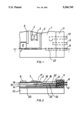
FIG. 1 is a plan view of the thick film hybrid arrangement in accordance with the present invention; and
FIG. 2 is a view showing a section of the inventive hybrid arrangement of FIG. 1, taken along the line 2--2.
DESCRIPTION OF THE PREFERRED EMBODIMENT
A thick film hybrid arrangement shown in FIG. 1 has in its upper visible surface an upper wiring plane 1 with several conductor paths 2, 3, 4 and 5 which are electrically connected with structural elements 6 and 7. Outer contacts 8, 9 and 10 extend outwardly beyond a right side of the thick layer hybrid arrangement on an injection molded insulation body 11. The insulation body 11 is composed of electrically insulating material and together with the outer contacts 8, 9, 10 and 12, shown in FIG. 2, forms a plug strip.
FIG. 2 shows a longitudinal section along the line 2--2. It can be seen there especially clearly that the thick layer hybrid arrangement has a support 13 composed of metal, and several conductor paths planes 14, 15 and 16 located on the support 13 and superposed over one another. Each of these planes is formed by conductor path placed on a ceramic foil 17, 18 and 19. The lower ceramic foil 17 is connected with the support 13 by an adhesive layer 20.
During the manufacture of the thick film hybrid arrangement in accordance with the present invention, the individual foils are successively placed over one another with the conductor path placed on them. For mounting of outer contacts 8, 9, 10, 12, wherein 9 and 10 are not shown, metal lugs 21 and 22 formed as metal sheet shaped parts are placed between the foils. In a subsequent sintering process the thick film hybrid arrangement is produced with the individual layers firmly connected with one another. The conductor paths 23 and 24 of the placed metal lugs 21 and 22 are electrically connected with the above mentioned conductor paths in an electrically conductive manner. Subsequently the lateral insulating body 11 is injection molded in a known synthetic plastic injection molding process, so that the extending outer contacts 8, 9, 10 and 12 are insulated from one another and mechanically fixed.
It is to be understood that the support 13 must not be entirely composed of metal. It can also be made of ceramic.
It will be understood that each of the elements described above, or two or more together, may also find a useful application in other types of constructions differing from the types described above.
While the invention has been illustrated and described as embodied in a thick film hybrid arrangement, it is not intended to be limited to the details shown, since various modifications and structural changes may be made without departing in any way from the spirit of the present invention.
Without further analysis, the foregoing will so fully reveal the gist of the present invention that others can, by applying current knowledge, readily adapt it for various applications without omitting features that, from the standpoint of prior art, fairly constitute essential characteristics of the generic or specific aspects of this invention.

Claims (8)

What is claimed as new and desired to be protected by Letters Patent is set forth in the appended claims:
1. A thick film hybrid arrangement comprising a plurality of ceramic foils provided with conductor paths and superimposed over one another; a support for supporting said ceramic foils; a plurality of thin metal lugs located between said ceramic foils for contacting said conducting paths, said metal lugs extending outwardly beyond at least said ceramic foils so as to form outer contacts; and an insulating body which directly adjoins said ceramic foils, said outer contacts being supported in said insulating body.
2. An arrangement as defined in claim 1, wherein said support is composed of metal.
3. An arrangement as defined in claim 1, wherein said support is composed of ceramic.
4. An arrangement as defined in claim 1, wherein said insulating body is formed as an injection molded synthetic plastic member.
5. A thick film hybrid arrangement, comprising a plurality of ceramic foils provided with conductor paths and superimposed over one another; a support for supporting said ceramic foils; and a plurality of thin metal lugs located between said ceramic foils for contacting said conducting paths, said metal lugs extending outwardly beyond at least said ceramic foils so as to form outer contacts, said metal lugs being formed as metal sheet shaped parts.
6. An arrangement as defined in claim 5, wherein said metal lugs have a thickness which increases outwardly.
7. A thick film hybrid arrangement, comprising a plurality of ceramic foils provided with conductor paths and superimposed over one another; a support for supporting said ceramic foils; and a plurality of thin metal lugs located between said ceramic foils for contacting said conducting paths, said metal lugs extending outwardly beyond at least said ceramic foils so as to form outer contacts, said metal lugs having a thickness of substantially 0.1 mm.
8. An arrangement as defined in claim 7, wherein said metal lugs have a thickness which increases outwardly from 0.1 mm to more than 0.2 mm.
US07/760,692 1990-10-04 1991-09-16 Thick film hybrid arrangement with outer contacts Expired - Fee Related US5266745A (en)

Applications Claiming Priority (2)

Application Number Priority Date Filing Date Title
DE4031203 1990-10-04
DE4031203A DE4031203A1 (en) 1990-10-04 1990-10-04 THICK LAYER HYBRID ARRANGEMENT WITH EXTERNAL CONTACTS

Publications (1)

Publication Number Publication Date
US5266745A true US5266745A (en) 1993-11-30

Family

ID=6415451

Family Applications (1)

Application Number Title Priority Date Filing Date
US07/760,692 Expired - Fee Related US5266745A (en) 1990-10-04 1991-09-16 Thick film hybrid arrangement with outer contacts

Country Status (3)

Country Link
US (1) US5266745A (en)
JP (1) JP3312036B2 (en)
DE (1) DE4031203A1 (en)

Cited By (3)

* Cited by examiner, † Cited by third party
Publication number Priority date Publication date Assignee Title
US20060027374A1 (en) * 2002-11-21 2006-02-09 Ludlow Jeremy L C Electrical transmission system
US20070003725A1 (en) * 2005-06-30 2007-01-04 Yousif Paul E Tabbed container seal and method of manufacture
JP2019121779A (en) * 2018-01-10 2019-07-22 サムソン エレクトロ−メカニックス カンパニーリミテッド. Printed circuit board and battery module including the same

Citations (5)

* Cited by examiner, † Cited by third party
Publication number Priority date Publication date Assignee Title
US3585455A (en) * 1968-01-26 1971-06-15 Ferranti Ltd Circuit assemblies
US4401844A (en) * 1980-11-28 1983-08-30 L.C.C.-C.I.C.E.-Compagnie Europeenne De Composants Electroniques Power supply bar comprising a stack of 2 n metal layers separated by 2 n dielectric layers
US4827328A (en) * 1986-03-17 1989-05-02 Fujitsu Limited Hybrid IC device
US4835394A (en) * 1987-07-31 1989-05-30 General Electric Company Cable assembly for an electrical signal transmission system
US5051542A (en) * 1988-08-01 1991-09-24 Rogers Corporation Low impedance bus bar

Patent Citations (5)

* Cited by examiner, † Cited by third party
Publication number Priority date Publication date Assignee Title
US3585455A (en) * 1968-01-26 1971-06-15 Ferranti Ltd Circuit assemblies
US4401844A (en) * 1980-11-28 1983-08-30 L.C.C.-C.I.C.E.-Compagnie Europeenne De Composants Electroniques Power supply bar comprising a stack of 2 n metal layers separated by 2 n dielectric layers
US4827328A (en) * 1986-03-17 1989-05-02 Fujitsu Limited Hybrid IC device
US4835394A (en) * 1987-07-31 1989-05-30 General Electric Company Cable assembly for an electrical signal transmission system
US5051542A (en) * 1988-08-01 1991-09-24 Rogers Corporation Low impedance bus bar

Cited By (4)

* Cited by examiner, † Cited by third party
Publication number Priority date Publication date Assignee Title
US20060027374A1 (en) * 2002-11-21 2006-02-09 Ludlow Jeremy L C Electrical transmission system
US20070003725A1 (en) * 2005-06-30 2007-01-04 Yousif Paul E Tabbed container seal and method of manufacture
JP2019121779A (en) * 2018-01-10 2019-07-22 サムソン エレクトロ−メカニックス カンパニーリミテッド. Printed circuit board and battery module including the same
JP7115666B2 (en) 2018-01-10 2022-08-09 サムソン エレクトロ-メカニックス カンパニーリミテッド. Printed circuit board and battery module containing same

Also Published As

Publication number Publication date
JP3312036B2 (en) 2002-08-05
DE4031203A1 (en) 1992-04-09
JPH04247650A (en) 1992-09-03

Similar Documents

Publication Publication Date Title
US4266091A (en) Layer-built laminated bus embedding condensers
US4164778A (en) Printed circuit board
US5539618A (en) Electrical device, in particular switching or controlling device for motor vehicle
KR890702161A (en) Integrated circuit device and manufacturing method thereof
KR890016588A (en) Chip Resistor and Manufacturing Method
US3183407A (en) Combined electrical element
US5253148A (en) Electric double layer capacitor
US3114807A (en) Sealed switch unit mounted on printed circuit board
US5119272A (en) Circuit board and method of producing circuit board
US4570031A (en) High capacitance laminated buss and method of manufacture
US3118095A (en) Capacitor and terminal therefor
US5266745A (en) Thick film hybrid arrangement with outer contacts
US3346774A (en) Electrical component substrate with cavities for anchoring lead wires therein
US4933811A (en) Direct-transfer electrical component
US2990498A (en) Capacitor
JPS6210984Y2 (en)
JPS6133246B2 (en)
JPH0888103A (en) Surface-mounted electronic component
US4507710A (en) Electronic components and system carrier assembly
US20230411077A1 (en) Electronic device
JPS5846836B2 (en) connector
US20230061638A1 (en) Electronic device
US3238597A (en) Method of making a miniature wound capacitor
US3330995A (en) High density electric structure awx mtthoii of kaking
JPS61113223A (en) Leadless type electrolytic capacitor

Legal Events

Date Code Title Description
AS Assignment

Owner name: ROBERT BOSCH GMBH

Free format text: ASSIGNMENT OF ASSIGNORS INTEREST.;ASSIGNOR:SEIPLER, DIETER;REEL/FRAME:005850/0085

Effective date: 19910904

FEPP Fee payment procedure

Free format text: PAYOR NUMBER ASSIGNED (ORIGINAL EVENT CODE: ASPN); ENTITY STATUS OF PATENT OWNER: LARGE ENTITY

FPAY Fee payment

Year of fee payment: 4

REFU Refund

Free format text: REFUND - PAYMENT OF MAINTENANCE FEE, 8TH YEAR, LARGE ENTITY (ORIGINAL EVENT CODE: R184); ENTITY STATUS OF PATENT OWNER: LARGE ENTITY

FPAY Fee payment

Year of fee payment: 8

REMI Maintenance fee reminder mailed
LAPS Lapse for failure to pay maintenance fees
STCH Information on status: patent discontinuation

Free format text: PATENT EXPIRED DUE TO NONPAYMENT OF MAINTENANCE FEES UNDER 37 CFR 1.362

FP Lapsed due to failure to pay maintenance fee

Effective date: 20051130