US5280156A - Wafer heating apparatus and with ceramic substrate and dielectric layer having electrostatic chucking means - Google Patents
Wafer heating apparatus and with ceramic substrate and dielectric layer having electrostatic chucking means Download PDFInfo
- Publication number
- US5280156A US5280156A US07/811,946 US81194691A US5280156A US 5280156 A US5280156 A US 5280156A US 81194691 A US81194691 A US 81194691A US 5280156 A US5280156 A US 5280156A
- Authority
- US
- United States
- Prior art keywords
- wafer
- dielectric layer
- ceramic
- ceramic substrate
- film electrode
- Prior art date
- Legal status (The legal status is an assumption and is not a legal conclusion. Google has not performed a legal analysis and makes no representation as to the accuracy of the status listed.)
- Expired - Lifetime
Links
Images


Classifications
-
- H—ELECTRICITY
- H01—ELECTRIC ELEMENTS
- H01L—SEMICONDUCTOR DEVICES NOT COVERED BY CLASS H10
- H01L21/00—Processes or apparatus adapted for the manufacture or treatment of semiconductor or solid state devices or of parts thereof
- H01L21/67—Apparatus specially adapted for handling semiconductor or electric solid state devices during manufacture or treatment thereof; Apparatus specially adapted for handling wafers during manufacture or treatment of semiconductor or electric solid state devices or components ; Apparatus not specifically provided for elsewhere
- H01L21/67005—Apparatus not specifically provided for elsewhere
- H01L21/67011—Apparatus for manufacture or treatment
- H01L21/67098—Apparatus for thermal treatment
- H01L21/67103—Apparatus for thermal treatment mainly by conduction
-
- H—ELECTRICITY
- H01—ELECTRIC ELEMENTS
- H01L—SEMICONDUCTOR DEVICES NOT COVERED BY CLASS H10
- H01L2924/00—Indexing scheme for arrangements or methods for connecting or disconnecting semiconductor or solid-state bodies as covered by H01L24/00
- H01L2924/0001—Technical content checked by a classifier
- H01L2924/0002—Not covered by any one of groups H01L24/00, H01L24/00 and H01L2224/00
-
- Y—GENERAL TAGGING OF NEW TECHNOLOGICAL DEVELOPMENTS; GENERAL TAGGING OF CROSS-SECTIONAL TECHNOLOGIES SPANNING OVER SEVERAL SECTIONS OF THE IPC; TECHNICAL SUBJECTS COVERED BY FORMER USPC CROSS-REFERENCE ART COLLECTIONS [XRACs] AND DIGESTS
- Y10—TECHNICAL SUBJECTS COVERED BY FORMER USPC
- Y10T—TECHNICAL SUBJECTS COVERED BY FORMER US CLASSIFICATION
- Y10T279/00—Chucks or sockets
- Y10T279/23—Chucks or sockets with magnetic or electrostatic means
Definitions
- the present invention relates to a wafer heating apparatus for use in semiconductor producing systems, and methods for producing the same.
- a wafer heating apparatus of an indirect heating system which provides an infrared radiation arranged outside of a container wherein a wafer is exposed to the deposition gas, etc., a window on an outside wall of the container for permeating an infrared radiation emitted from the lamp therethrough into the container, and a heating body made of a highly corrosion resistant material, such as graphite, for irradiating a wafer mounted on the upper surface of the heating body by the infrared radiation to heat the wafer.
- a highly corrosion resistant material such as graphite
- this type of wafer heating apparatus has problems in that a large heat loss and a long heating time are required for temperature elevation, permeation of the infrared radiation is gradually prevented by a CVD film deposited on the window which causes the window to heat due to heat absorption thereof, and homogeneity and response of heating become bad due to the separate provision of the heating source lamp and the heating body mounting the wafer.
- a mechanical fixing system for example, in transportation, light-exposure, film formation, fine machining, rinsing, dicing, etc., of semiconductor wafers.
- film preparing, processes, productivity i.e., yield of production of semiconductors is decreased at the time of producing the semiconductor wafers, if a surface temperature of the semiconductor wafer is not heated homogeneously.
- the formed film becomes uneven due to contact of a pin or a ring to the surface of the semiconductor wafer. If the semiconductor wafer is arranged at a heating surface of a disc-shaped ceramic heater, the whole surface of the semiconductor wafer is not uniformly urged against the flat surface of the heater disc, so that the semiconductor wafer is deflected and distorted to form a local gap between a portion of the semiconductor wafer and the flat heating surface of the ceramic heater disc.
- the behavior of decreased number of the gas molecules changes to a molecules-flowing region to widely decrease the heat flow due to the heat transfer of the gas molecules, so that the wafer temperature is decreased as compared with the heater temperature to worsen homogeneity and the response property of the heating.
- a vacuum chuck system is adopted for fixing the wafer, the system can not be used for sputtering, CVD or the like processes which are used under a condition of medium or high vacuum.
- electrostatic chucks using a polyimide film as a dielectric film in the so-called electrostatic chucks
- a usable temperature range of conventional electrostatic chucks is around 80°-200° C. at the maximum. Therefore, the electrostatic chuck can not be adopted for fixing the wafer in a sputtering or a CVD process wherein the wafer is heated by a heating element up to a temperature of about 600° C.
- An object of the present invention is to provide a wafer heating apparatus which can obviate a problem of contamination as seen in the case of using a metallic heater and the above problems of decreasing the heat efficiency as seen in the indirect wafer heating system, and which can improve homogeneity of heating of the wafer.
- the present invention is a wafer heating apparatus including a ceramic substrate, a heat-generating resistive element embedded in the interior of the ceramic substrate, a film electrode formed on a front surface of the ceramic substrate, and a ceramic dielectric layer formed on the front surface of the ceramic substrate to coat the film electrode, comprising a direct current power source which generates Coulomb's force between a wafer and a wafer-attracting surface of the dielectric layer to attract the wafer to the wafer-attracting surface, while heating the wafer by heat generation of the heat-generating resistive element.
- both the ceramic substrate and the ceramic dielectric layer are made of a same or different non-oxide series ceramic material.
- the ceramic substrate may have a coefficient of thermal expansion of 0.7-1.4 times that of the wafer.
- the ceramic dielectric layer may have a coefficient of thermal expansion of 0.7-1.4 times of that of the wafer.
- the film electrode is made of an electrically conductive adhesive which joins the ceramic dielectric layer to the ceramic substrate, and at least one electric terminal is connected to the film electrode.
- a heat generating resistive element is embedded and heated in the interior of a ceramic green sheet to prepare a ceramic substrate having the heat generating resistive element embedded therein, a ceramic green sheet is sintered to prepare a ceramic dielectric layer, the ceramic dielectric layer is joined to the front surface of the ceramic substrate by means of a film electrode made of an electrically conductive adhesive, and at least one electric terminal is connected to the film electrode.
- the film electrode is joined to a surface of the ceramic dielectric layer, a surface of the film electrode of the ceramic dielectric layer is joined to a front surface of the ceramic substrate, and at least one electric terminal is connected to the film electrode.
- a heat generating resistive element is embedded and heated in the interior of a ceramic green sheet to prepare a ceramic substrate having the heat generating resistive element embedded therein, a ceramic green sheet is sintered to prepare a ceramic dielectric layer, at least one film electrode is formed on a surface of the ceramic dielectric layer, a surface of the film electrode of the ceramic dielectric layer is joined to the front surface of the ceramic substrate by means of the film electrode made of an electrically insulative adhesive, and at least one electric terminal is connected to the film electrode.
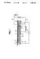
- FIG. 1 is a schematic partial cross-sectional view of an example of the present wafer heating apparatus
- FIG. 2 is a schematic cross-sectional view of the present wafer heating apparatus before assembling
- FIG. 3 is a schematic cross-sectional view of an example of the present wafer heating apparatus 1A;
- FIG. 4 is a schematic cross-sectional view of a dielectric layer on which a film electrode 5B is formed on a surface of the recess 4c of the dielectric layer;
- FIG. 5 is a schematic cross-sectional view of a dielectric layer wherein an electrically insulative adhesive layer 15 is formed on the surface of the film electrode 5B formed on the recess 4c of the dielectric layer;
- FIG. 6 is a schematic cross-sectional view of a substrate 2A joined to a dielectric layer 4A via an electrically insulative adhesive layer 15 and a film electrode 5B;
- FIG. 7 is a schematic cross-sectional view of the substrate 2A of FIG. 6 wherein a portion of the electrically insulative adhesive layer 15 is peeled off;
- FIG. 8 is a cross-sectional view of the substrate 2A to which a columnar terminal 7A is inserted and joined to the substrate 2A;
- FIG. 9 is a cross-sectional view of the wafer heating apparatus 1C of an embodiment of the present invention.
- a ceramic substrate 2 of a disc shape for example, is provided with a heat generating resistive element 3 embedded in the interior thereof, and the heat generating resistive element 3 is preferably wound in a spiral shape.
- the heat generating resistive element 3 is arranged in a whirl fashion.
- the heat generating resistive element 3 has at both ends thereof 8 connected and fixed thereto respectively for supplying an electric power thereto, and the ends of the respective terminal 8 are connected to a pair of electric power supply cables 9.
- the pair of cables 9 is respectively connected to a heater power source 10, and can energize the heat generating resistive element 3 upon closing a switch not shown.
- the ceramic substrate disc 2 has opposing front surfaces 2a, 2b at both sides.
- the word "front surface” used herein means a surface relatively broader than the other surfaces.
- the ceramic substrate disc 2 has a circular (for example) film electrode 5 formed along a front surface 2a thereof.
- a ceramic dielectric layer 4 is integrally formed on the front surface 2a so as to coat the film electrode 5.
- the film electrode 5 is accommodated between the ceramic substrate disc 2 and the ceramic dielectric layer 4. If the film electrode 5 has a perforated shape like a punching metal, coherence of the ceramic dielectric layer 4 to the film electrode 5 is improved.
- the ceramic substrate 2 has a terminal 7 embedded therein, one end of the terminal 7 is connected to the film electrode 5, and the other end of the terminal 7 is connected to a cable 11.
- the cable 11 is connected to the positive electrode of a power source 12 of an electrostatic chuck, and the negative electrode of the direct current power source 12 is connected to an earth wire 13.
- the wafer W When heat treating a wafer W, the wafer W is mounted on a wafer-attracting surface 6 of the ceramic dielectric layer 4, and the wafer W is contacted with the earth wire 13. Then, a positive electric charge is accumulated on the film electrode 5 to polarize the ceramic dielectric layer 4 and a positive electric charge is accumulated on the wafer-attracting surface 6 of the ceramic dielectric layer 4, while a negative electric charge is accumulated on the wafer W, so as to attract the wafer W to the wafer-attracting surface 6 of the ceramic dielectric layer 4 by Coulomb's attracting force between the ceramic dielectric layer 4 and the wafer W. In the meantime, the heat generating resistive element 3 is energized to heat the wafer-attracting surface 6 to a desired temperature.
- the wafer W can be heated through heating of the wafer-attracting surface 6, while attracting the whole surface of the wafer W to the wafer-attracting surface 6 by Coulomb's force.
- the whole surface of the wafer W shows a good response to the heating temperature of the apparatus and the wafer W can be heated uniformly, so that the decrease of the homogeneity of temperature caused by a gap between the wafer and the wafer heating surface 6 in heating the wafer W can be obviated. Therefore, the whole surface of the wafer W can be heated uniformly at the time of heating the wafer W, so that decrease of the production yield of semiconductors, for example, can be prevented in semiconductor production systems.
- the dielectric layer 4 is also made of a ceramic material, so that the dielectric layer 4 has also a high heat resistant property and can be used well in a thermal CVD system, for example.
- the dielectric layer 4 is made of a ceramic material which has a high endurance to repeated abrasion and deformation of more than 10,000 times caused by the electrostatic chuck of the wafer W.
- the heat generating resistive element 3 is embedded in the interior of the ceramic substrate 2 and the film electrode 5 is accommodated between the ceramic dielectric layer 4 and the ceramic substrate 2, the contamination caused by a conventional metallic heater can be prevented. Moreover, the wafer W is directly heated at a state of being attracted to the wafer-attracting surface 6, so that the problem of decrease of heat efficiency occurring in the indirect heating system can be obviated.
- the dielectric layer 4 is made of a ceramic material which has a characteristic property that an insulation resistance value (volumetric resistivity) is decreased with an increase of the ceramic temperature, the dielectric layer 4 may sometimes have a lower insulation resistance value than an appropriate insulation value of, e.g., around 10 11 ⁇ cm to allow a large leak current to flow.
- the dielectric layer 4 has preferably an insulation resistance value of not less than 10 11 ⁇ cm even at a high temperature range of, e.g., 500°-600° C. for use in the wafer heating apparatus 1 of this embodiment.
- alumina, beryllia, magnesia, silicon nitride (reaction sintered, or ambient pressure sintered), boron nitride, or aluminum nitride is preferably used.
- the ceramic substrate 2 and the dielectric layer 4 are heated to a temperature of around 600°-1,100° C. at the maximum in a system, such as a thermal CVD system, so that they are preferably made of alumina, silicon nitride sintered body, sialon, silicon carbide, aluminum nitride, alumina-silicon carbide complex compound, etc. from a viewpoint of heat resistant property.
- a system such as a thermal CVD system
- the ceramic substrate 2 and the ceramic dielectric layer 4 are both made of the same or different non-oxide series ceramic material.
- the non-oxide series ceramic materials having a covalent bond such as SiC, Si 3 N 4 , etc.
- oxide-series ceramic materials such as alumina, etc.
- the non-oxide series ceramic materials can provide a small change of the voltage of withstanding insulation breakage and resistance value, etc., of the dielectric layer, as well as stable operation of the heater and the electrostatic chuck.
- the whole wafer heating apparatus 1 has a high strength and a high thermal shock resistant property by virtue of a low coefficient of thermal expansion of the silicon nitride, so that the wafer heating apparatus 1 is not destructed even in a repeated rapid heating to a high temperature and quenching therefrom. Because silicon nitride has a superior corrosion resistant property, the wafer heating apparatus 1 has a high durability and a long life even in a corrosive gas condition, such as in a thermal CVD system.
- the ceramic substrate 2 and the ceramic dielectric layer 4 are preferably made of the same material having the same thermal expansion from an aspect of coherence, and silicon nitride is preferable for such purpose because of both properties thereof as a heater and an electrostatic chuck.
- Both the coefficients of thermal expansion of the ceramic substrate 2 and the ceramic dielectric layer 4 are preferably 0.7-1.4 times of that of the wafer W. If they are beyond this range, the wafer W is cohered to the wafer-attracting surface 6 at the time of heating the wafer W, so that the wafer W is likely deformed. Combination of the materials of the substrate 2 and the dielectric layer 4 should be changed depending on the material of the wafer W. Particularly, if the wafer W is made of silicon having a coefficient of thermal expansion of 2.6 ⁇ 10 -6 K -1 , the coefficients of thermal expansion thereof are preferably within a range of 1.82 ⁇ 10 -6 -3.38 ⁇ 10 -6 K -1 .
- silicon nitride has a coefficient of thermal expansion of 2.7 ⁇ 10 -6 K -1 , it is most suited to the materials of the ceramic substrate 2 and the ceramic dielectric layer 4. This is because under a condition of an attracting force of not more than 100 kg/cm 2 for attracting the wafer W in vacuum, if alumina having a high coefficient of thermal expansion (7 ⁇ 10 -6 K -1 ) is used, the wafer having a thickness of about 0.6 mm is forecasted to deform around 0.25% due to restrainment of the electrostatic chuck, so that damage of the wafer due to the deformation is quite large.
- the wafer-attracting surface 6 is preferably a smooth flat surface and preferably has a flat surface degree of not more than 500 ⁇ m so as to prevent invasion of the deposition gas to the backside of the wafer W.
- the heat generating resistive element 3 use of tungsten, molybdenum, platinum, etc., having a high melting point and a superior coherent property to silicon nitride, etc., is appropriate.
- FIGS. 2 and 3 respectively of a cross-sectional view of the present wafer heating apparatus of this embodiment before and after assembling, an embodiment is shown wherein a ceramic dielectric layer 4A of a flat disc shape is prepared by sintering a ceramic green sheet.
- the ceramic dielectric layer disc 4A has a ring shaped flange portion 4b formed at its circumferential periphery, and the flange portion 4b has a disc shaped recess 4c at the inner side thereof.
- a sheet disc 5A made of an electrically conductive adhesive is prepared which functions also as a film electrode 5A as described below.
- a disc shaped ceramic substrate 2A is prepared by sintering a ceramic green sheet.
- the ceramic green sheet 2A has at its central portion a circular penetration hole 14 for receiving a terminal 7A inserted therein.
- a front surface 2a of the ceramic substrate 2A is opposing to the film electrode 5A.
- a pair or a massive terminals 8A are exposed on the other front surface 2b of the ceramic 2A.
- Each terminal 8A is embedded in the ceramic substrate 2A and connected to the heat generating resistive element 3.
- the heat generating resistive element 3 is embedded in a swirl pattern, more particularly in a spiral form in the disc shaped ceramic substrate 2A. Also, a columnar terminal 7A is prepared.
- the ceramic dielectric layer 4A For forming the ceramic dielectric layer 4A, press forming, or tape cast forming, etc., can be used.
- the heat generating resistive element 3 and the terminals 8 are embedded in a ceramic material which is then formed by press forming, or cold isostatic press forming, etc., and sintered by hot press sintering, or hot isostatic press sintering, etc.
- the film electrode 5A is accommodated in the recess 4c so as to abut to the surface of the dielectric layer 4A, and the front surface 2a of the ceramic substrate 2A is abutted to the surface of the film electrode 5A.
- the columnar terminal 7A is inserted in the penetration hole 14 and an end surface 7a of the columnar terminal 7A is abutted to the film electrode 5A.
- a powdery adhesive is interposed between the wall surface of the penetration hole 14 and the side circumferential wall of the columnar terminal 7A.
- the thus obtained assembly is subjected to a heat treatment to join the dielectric layer 4A and the substrate 2A by means of the film electrode 5A made of the electrically conductive adhesive, as shown in FIG. 3.
- the columnar terminal 7A is joined and fixed to the penetration hole 14 of the substrate 2A.
- the surface of the dielectric layer 4A is worked by grinding to smoothen the wafer-attracting surface 6.
- An end surface 7b of the columnar terminal 7 is connected to a cable 11 and the cable 11 is connected to the positive electrode of a power source 12 of an electrostatic chuck, and the negative electrode of the power source 12 are connected to an earth wire 13.
- the pair of terminals 8A is connected respectively to the cable 9 and the cables 9 are connected to a heater power source 10.
- the wafer W For attracting a wafer W, the wafer W is mounted on the wafer-attracting surface 6 and the earth wire 13 is contacted with the wafer W. Then, an electric positive charge is accumulated on the film electrode 5A to polarize the the dielectric layer 4A, and an electric positive charge is accumulated on the wafer-attracting surface 6 of the dielectric layer 4A. At the same time, a negative electric charge is accumulated on the wafer W to attract the wafer W to the wafer-attracting surface 6 by Coulomb's force between the dielectric layer 4A and the wafer W. Simultaneously, the heating resistive element 3 is energized to heat the wafer W.
- the sintered dielectric layer 4A and the substrate 2A joined by means of the electrically conductive adhesive and the formed electrically conductive layer in situ is used as the film electrode, so that a need of providing an electrode plate, etc., can be dispensed with, the structure is quite simple, and production steps can be decreased.
- the wafer heating apparatus has the flange portion 4b, a discharge of electric current is not formed between the film electrode 5A and the semiconductor wafer W even at a high or medium vacuum condition of, for example, not more than 10 -3 Torr.
- this example has a large characteristic feature in the production method of the apparatus. This point will be explained in more detail in sequence, hereinafter.
- the thickness of the dielectric layer 4 is usually very thin of not more than 400 ⁇ m, so that the wafer-attracting forces on the wafer-attracting surface 6 fractured even when the thicknesses were fractured on the order of a few tens of ⁇ m. Particularly, a purposed wafer-attracting force was not obtained on the dielectric layer 4 at relatively thick portions, so that sometimes correction of deflection of the wafer became insufficient.
- insulation withstanding voltage of the dielectric layer 4 locally decreased at relatively thin portions thereof. Because the insulation withstanding voltage-decreased portion determined the insulation withstanding voltage of the final product wafer heating apparatus, the insulation withstanding voltage of the whole product was sometimes extremely decreased.
- a wafer was set to a use condition of a temperature of 450° C. and a molecular flow region of a vacuum of not more than 10 -3 Torr.
- a temperature of the wafer fixed by the electrostatic chuck was monitored by an infrared radiation thermometer, a local region was formed of a different temperature from that of the surrounding regions so that the required homogeneity (of ⁇ 3° C.) of heating temperature was not acquired.
- the temperature difference reached sometimes more than 150° C., as the case may be.
- the dielectric layer was broken due to thermal stress.
- the dielectric layer 4A is prepared by sintering of the ceramic green sheet and the sintering shrinkage has already been finished at the sintering stage, so that the dielectric layer 4A is deformed no further at the step of joining it to the ceramic substrate 2A.
- the thickness of the dielectric layer 4A can be made exactly uniform by working the surface of the dielectric layer 4A to a smooth surface. Therefore, a local decrease of the wafer-attracting force and a local decrease of the insulation withstanding voltage can not occur. Moreover, because the gaps caused by sintering shrinkage are not formed between the dielectric layer 4A and the ceramic substrate 2A, a superior uniform heating and a beautiful thermal shock resistant property of the dielectric layer 4A can be obtained.
- Example 1 The same materials as those described in Example 1 may be used as materials of the ceramic substrate 2A and the dielectric layer 4A of this example.
- the material of the columnar terminal 7A Kovar, tungsten, molybdenum, platinum, titanium, and nickel, etc., can be used.
- an adhesive such as a gold solder containing a titanium component, or a silver solder containing a titanium component, is preferable. This is because the titanium component contained in the solder diffuses into the ceramic materials by the heat treatment to improve the joining force of the respective ceramic members. These adhesives have a good joining property particularly to silicon nitride. Though in a wafer heating apparatus which uses a temperature of not less than 300° C.
- the dielectric layer 4A sometimes suffers from thermal shock when the wafer of an ambient temperature is transferred thereto by a transferring robot and fixed by the chuck and heated to the temperature, the thermal shock resistant property of the wafer heating apparatus is further improved due to relaxation of a stress by plastic deformation of the used solder, for example, the gold solder containing the titanium component.
- the wafer heating apparatus 1A was produced following the process steps shown in FIGS. 2 and 3 except that the dielectric layer 4A and the substrate 2A were respectively made of silicon nitride and prepared by hot press sintering at 1850° C.
- the terminals 8A and the heat generating resistive element 3 are made of tungsten.
- a sheet disc 5A of a thickness of 100 ⁇ m was prepared having a composition of 71.2 wt. % of silver, 27.9 wt. % of copper and 0.8 wt. % of titanium.
- a powdery silver solder having the same composition with the disc was interposed between the columnar terminal 7A and the penetration hole 14.
- the obtained assembly was heat treated in a hot press firing furnace while applying a pressure of not less than 50 g/cm 2 in the vertical direction of FIG. 2 to perform soldering of the columnar terminal 7A and the penetration hole 14.
- the soldering was effected in an atmosphere of a pressure of not more than 10 -5 Torr.
- the heat treatment was effected at 900° C. for 60 seconds. Temperature increase or decrease to the maximum temperature of 900° C. was preferably performed as quickly as possible within such a range that the ceramic materials were not destroyed due to thermal shock. In this example, a temperature increasing or decreasing rate of 600° C./hr was used because of the use of silicon nitride having a high thermal shock resistant property.
- the wafer heating apparatus 1A after being heat treated was taken out from the heating furnace and the surface of the dielectric layer 4A was worked by grinding to adjust the thickness thereof to 300 ⁇ m, for example.
- FIGS. 4-8 production steps for producing another embodiment of the present wafer heating apparatus 1B will be explained hereinafter, wherein the same reference numerals as those of FIGS. 2 and 3 are used for the same members having the same function and the explanations thereof are omitted, as the case may be.
- the film electrode 5B is formed on the surface of recess 4c of the dielectric layer 4A, as shown in FIG. 4.
- an electrically insulative adhesive layer 15 is applied on the recess 4c by coating, etc., as shown in FIG. 5. At this time, the film electrode 5B is coated with the electrically insulative adhesive layer 15.
- the substrate 2A having a disc shape as shown in FIG. 6 is inserted in the recess 4c to abut the surface of the substrate 2A to the electrically insulative adhesive layer 15 as shown in FIG. 5.
- the thus obtained assembly is heat treated to join the front surface 2a of the substrate 2A and the surface of the dielectric layer 4A having the film electrode 5B thereon as shown in FIG. 6 by means of the heat treated electrically insulative adhesive layer 15.
- the electrically insulative adhesive layer 15 is circularly peeled off at the penetration hole 14 to form a circular peeled-off portion 15a, thereby to expose a portion of the surface of the film electrode 5B corresponding to the circular peeled-off portion 15a to the penetration hole 14, as shown in FIG. 7.
- a wafer heating apparatus was produced in practice according to the production steps shown in FIGS. 4-8, except that the film electrode 5B was produced by screen printing of tungsten, and the dielectric layer 4A after formation of the film electrode 5B thereon was heated to a temperature of not less than 120° C. to evaporate an organic solvent remaining in the printed film electrode 5B.
- Both the dielectric layer 4A and the substrate 2A were made of silicon nitride.
- the film electrode 5B is alternatively made of molybdenum, or tungsten, etc.
- a sealing glass was used as the electrically insulative adhesive. More concretely explained, an oxynitride glass of the following composition was used.
- the substrate 2A and the dielectric layer 4A are heated in nitrogen atmosphere at 1,500° C. under a pressure of not less than 50 g/cm 2 in a hot press firing furnace.
- a powder of a titanium vapor deposited silver solder consisting of 71.3 wt. % of silver, 27.9 wt. % of copper and 0.8 wt. % of titanium was used.
- the soldering was effected in an atmosphere of a pressure of not more than 10 -5 Torr.
- the heat treatment was effected at 900° C. for 60 sec in a furnace.
- a temperature increasing or decreasing rate to the maximum temperature of 900° C. was 600° C./hr.
- the treated wafer heating apparatus was taken out from the heating furnace and worked by grinding at the surface of the dielectric layer 4A to adjust the thickness thereof to, for example, 300 ⁇ m.
- the terminal 8A and the heat generating resistive element 3 were formed of tungsten.
- FIG. 9 An example of a dipolar type wafer heating apparatus 1c is shown in FIG. 9.
- the ceramic substrate disc 2B is provided with two circular penetration holes 14 each having the columnar terminal 7A inserted and fixed therein.
- Two flat circular film electrodes 5C are formed on the surface of the recess 4c. To the central portion of each film electrode 5C is respectively abutted the end surface 7a of the terminal 7A.
- the left terminal 7A in FIG. 9, is connected to the negative electrode of the direct current power source 12A, and the positive electrode of the direct current power source 12A is grounded to the earth.
- the right terminal 7A in FIG. 9, is connected to the positive electrode of the direct current power source 12B, and the negative electrode of the direct current power source 12B is grounded to the earth.
- the wafer-attracting surface 6 is shown as facing upward, however, the wafer-attracting surface 6 may be faced downward.
- the whole shape of the wafer heating apparatus is preferably a disc shape for uniformly heating the circular wafer W.
- other shapes such as square, hexagonal, may also be used.
- Such wafer heating apparatus is usable as a wafer heating apparatus in an epitaxial system, a plasma etching system, or a photoetching system, etc.
- the wafer W is not solely restricted to a semiconductor wafer, and other conductor wafers, such as AL wafer, or Fe wafer, etc., may be subjected to the wafer attracting and heating treatment.
- a film electrode is formed on a front surface of the ceramic substrate, a ceramic dielectric layer is formed on the front surface of the ceramic substrate to coat the film electrode, and both the substrate and the dielectric layer are made of ceramic materials, so that the wafer heating apparatus can also be used to high temperature usages, such as thermal CVD system, etc., when attracting the wafer to the wafer-attracting surface of the ceramic dielectric layer.
- the heat generating resistive element is embedded in the interior of the ceramic substrate and heat generated under energization to heat the wafer, so that the wafer is attracted at the whole surface to the wafer-attracting surface of the ceramic dielectric layer by Coulomb's force and simultaneously heated at the whole surface via the wafer-attracting surface.
- the wafer can be easily heated uniformly at the whole surface, so that the occurrence of local gaps between the wafer and the wafer-attracting surface (i.e., the wafer-heating surface) at the time of heating the wafer can be prevented. Therefore, production yield of wafers at the time of heating the wafers can be exceedingly improved.
- the heat generating resistive element is heat generated at the state of attracting the wafer to the wafer-attracting surface of the ceramic dielectric layer to directly heat the wafer by the wafer-attracting surface, so that a high heat efficiency can be obtained at the heating.
Abstract
Description
Claims (6)
Applications Claiming Priority (4)
| Application Number | Priority Date | Filing Date | Title |
|---|---|---|---|
| JP2-418006 | 1990-12-25 | ||
| JP41800690 | 1990-12-25 | ||
| JP3-303289 | 1991-11-19 | ||
| JP30328991A JPH0750736B2 (en) | 1990-12-25 | 1991-11-19 | Wafer heating apparatus and manufacturing method thereof |
Publications (1)
| Publication Number | Publication Date |
|---|---|
| US5280156A true US5280156A (en) | 1994-01-18 |
Family
ID=26563477
Family Applications (1)
| Application Number | Title | Priority Date | Filing Date |
|---|---|---|---|
| US07/811,946 Expired - Lifetime US5280156A (en) | 1990-12-25 | 1991-12-23 | Wafer heating apparatus and with ceramic substrate and dielectric layer having electrostatic chucking means |
Country Status (3)
| Country | Link |
|---|---|
| US (1) | US5280156A (en) |
| EP (1) | EP0493089B1 (en) |
| DE (1) | DE69130205T2 (en) |
Cited By (193)
| Publication number | Priority date | Publication date | Assignee | Title |
|---|---|---|---|---|
| US5382469A (en) * | 1992-06-26 | 1995-01-17 | Shin-Etsu Chemical Co., Ltd. | Ceramic-titanium nitride electrostatic chuck |
| US5407487A (en) * | 1993-05-05 | 1995-04-18 | Weber Manufacturing Limited | Method and apparatus for producing nickel shell molds |
| US5460684A (en) * | 1992-12-04 | 1995-10-24 | Tokyo Electron Limited | Stage having electrostatic chuck and plasma processing apparatus using same |
| KR960030365A (en) * | 1995-01-31 | 1996-08-17 | 제임스 조셉 드롱 | High temperature polyimide electrostatic chuck |
| US5554224A (en) * | 1994-03-31 | 1996-09-10 | Foltyn; Steve R. | Substrate heater for thin film deposition |
| US5560780A (en) * | 1993-04-22 | 1996-10-01 | Applied Materials, Inc. | Protective coating for dielectric material on wafer support used in integrated circuit processing apparatus and method of forming same |
| US5566043A (en) * | 1993-12-27 | 1996-10-15 | Shin-Etsu Chemical Co., Ltd. | Ceramic electrostatic chuck with built-in heater |
| US5600530A (en) * | 1992-08-04 | 1997-02-04 | The Morgan Crucible Company Plc | Electrostatic chuck |
| US5606484A (en) * | 1993-06-23 | 1997-02-25 | Shin-Etsu Chemical Co., Ltd. | Ceramic electrostatic chuck with built-in heater |
| US5618350A (en) * | 1995-03-23 | 1997-04-08 | Tokyo Electron Limited | Processing apparatus |
| US5633073A (en) * | 1995-07-14 | 1997-05-27 | Applied Materials, Inc. | Ceramic susceptor with embedded metal electrode and eutectic connection |
| US5668524A (en) * | 1994-02-09 | 1997-09-16 | Kyocera Corporation | Ceramic resistor and electrostatic chuck having an aluminum nitride crystal phase |
| US5671117A (en) * | 1994-02-28 | 1997-09-23 | Applied Materials Inc. | Electrostatic chuck |
| US5683606A (en) * | 1993-12-20 | 1997-11-04 | Ngk Insulators, Ltd. | Ceramic heaters and heating devices using such ceramic heaters |
| US5729423A (en) * | 1994-01-31 | 1998-03-17 | Applied Materials, Inc. | Puncture resistant electrostatic chuck |
| US5792562A (en) * | 1995-01-12 | 1998-08-11 | Applied Materials, Inc. | Electrostatic chuck with polymeric impregnation and method of making |
| US5801915A (en) * | 1994-01-31 | 1998-09-01 | Applied Materials, Inc. | Electrostatic chuck having a unidirectionally conducting coupler layer |
| US5800618A (en) * | 1992-11-12 | 1998-09-01 | Ngk Insulators, Ltd. | Plasma-generating electrode device, an electrode-embedded article, and a method of manufacturing thereof |
| US5817406A (en) * | 1995-07-14 | 1998-10-06 | Applied Materials, Inc. | Ceramic susceptor with embedded metal electrode and brazing material connection |
| US5835334A (en) * | 1996-09-30 | 1998-11-10 | Lam Research | Variable high temperature chuck for high density plasma chemical vapor deposition |
| US5883778A (en) * | 1994-02-28 | 1999-03-16 | Applied Materials, Inc. | Electrostatic chuck with fluid flow regulator |
| US5886866A (en) * | 1998-07-06 | 1999-03-23 | Applied Materials, Inc. | Electrostatic chuck having a combination electrode structure for substrate chucking, heating and biasing |
| US5886863A (en) * | 1995-05-09 | 1999-03-23 | Kyocera Corporation | Wafer support member |
| US5901030A (en) * | 1997-12-02 | 1999-05-04 | Dorsey Gage, Inc. | Electrostatic chuck employing thermoelectric cooling |
| US5946183A (en) * | 1995-09-06 | 1999-08-31 | Ngk Insulators, Ltd. | Electrostatic chuck |
| US5981913A (en) * | 1996-03-22 | 1999-11-09 | Sony Corporation | Static electricity chuck and wafer stage |
| US6051122A (en) * | 1997-08-21 | 2000-04-18 | Applied Materials, Inc. | Deposition shield assembly for a semiconductor wafer processing system |
| US6074488A (en) * | 1997-09-16 | 2000-06-13 | Applied Materials, Inc | Plasma chamber support having an electrically coupled collar ring |
| US6094334A (en) * | 1999-03-02 | 2000-07-25 | Applied Materials, Inc. | Polymer chuck with heater and method of manufacture |
| US6095084A (en) * | 1996-02-02 | 2000-08-01 | Applied Materials, Inc. | High density plasma process chamber |
| US6100506A (en) * | 1999-07-26 | 2000-08-08 | International Business Machines Corporation | Hot plate with in situ surface temperature adjustment |
| US6106630A (en) * | 1997-08-07 | 2000-08-22 | Applied Materials, Inc. | Ceramic-coated heating assembly for high temperature processing chamber |
| US6133557A (en) * | 1995-01-31 | 2000-10-17 | Kyocera Corporation | Wafer holding member |
| US6160244A (en) * | 1998-05-29 | 2000-12-12 | Ngk Insulators, Ltd. | Susceptors |
| US6183693B1 (en) * | 1998-02-27 | 2001-02-06 | Cytologix Corporation | Random access slide stainer with independent slide heating regulation |
| US6189482B1 (en) | 1997-02-12 | 2001-02-20 | Applied Materials, Inc. | High temperature, high flow rate chemical vapor deposition apparatus and related methods |
| US6204489B1 (en) * | 1998-01-09 | 2001-03-20 | Ngk Insulators, Ltd. | Electrically heated substrate with multiple ceramic parts each having different volume restivities |
| US6242719B1 (en) * | 1998-06-11 | 2001-06-05 | Shin-Etsu Handotai Co., Ltd. | Multiple-layered ceramic heater |
| US6263829B1 (en) | 1999-01-22 | 2001-07-24 | Applied Materials, Inc. | Process chamber having improved gas distributor and method of manufacture |
| US6278600B1 (en) | 1994-01-31 | 2001-08-21 | Applied Materials, Inc. | Electrostatic chuck with improved temperature control and puncture resistance |
| US20010019903A1 (en) * | 1996-12-23 | 2001-09-06 | Paul Kevin Shufflebotham | Inductively coupled plasma CVD |
| US6296809B1 (en) | 1998-02-27 | 2001-10-02 | Ventana Medical Systems, Inc. | Automated molecular pathology apparatus having independent slide heaters |
| US6310755B1 (en) | 1999-05-07 | 2001-10-30 | Applied Materials, Inc. | Electrostatic chuck having gas cavity and method |
| US20020043530A1 (en) * | 1999-11-19 | 2002-04-18 | Yasutaka Ito | Ceramic heater |
| US6376808B2 (en) * | 2000-05-12 | 2002-04-23 | Nhk Spring Co., Ltd. | Heating apparatus |
| US6377437B1 (en) | 1999-12-22 | 2002-04-23 | Lam Research Corporation | High temperature electrostatic chuck |
| US6410172B1 (en) * | 1999-11-23 | 2002-06-25 | Advanced Ceramics Corporation | Articles coated with aluminum nitride by chemical vapor deposition |
| US6414834B1 (en) | 1996-04-26 | 2002-07-02 | Applied Materials, Inc. | Dielectric covered electrostatic chuck |
| US6448538B1 (en) * | 1996-05-05 | 2002-09-10 | Seiichiro Miyata | Electric heating element |
| US6462928B1 (en) | 1999-05-07 | 2002-10-08 | Applied Materials, Inc. | Electrostatic chuck having improved electrical connector and method |
| US20020163350A1 (en) * | 2001-05-07 | 2002-11-07 | Jorg Kiesewetter | Substrate-holding device for testing circuit arrangements on substrates |
| US6478924B1 (en) | 2000-03-07 | 2002-11-12 | Applied Materials, Inc. | Plasma chamber support having dual electrodes |
| US6490144B1 (en) | 1999-11-29 | 2002-12-03 | Applied Materials, Inc. | Support for supporting a substrate in a process chamber |
| US6490146B2 (en) | 1999-05-07 | 2002-12-03 | Applied Materials Inc. | Electrostatic chuck bonded to base with a bond layer and method |
| US6494955B1 (en) | 2000-02-15 | 2002-12-17 | Applied Materials, Inc. | Ceramic substrate support |
| US6494958B1 (en) | 2000-06-29 | 2002-12-17 | Applied Materials Inc. | Plasma chamber support with coupled electrode |
| US20030000938A1 (en) * | 2000-12-01 | 2003-01-02 | Yanling Zhou | Ceramic heater, and ceramic heater resistor paste |
| US20030047589A1 (en) * | 2001-09-05 | 2003-03-13 | Ngk Insulators, Ltd. | Joined article of a supporting member for a semiconductor wafer and a method of producing the same |
| US6535371B1 (en) * | 1997-12-02 | 2003-03-18 | Takashi Kayamoto | Layered ceramic/metallic assembly, and an electrostatic chuck using such an assembly |
| US6538872B1 (en) | 2001-11-05 | 2003-03-25 | Applied Materials, Inc. | Electrostatic chuck having heater and method |
| US20030066608A1 (en) * | 2001-10-03 | 2003-04-10 | Sumitomo Electric Industries, Ltd. | Semiconductor processing apparatus and electrode member therefor |
| US20030098299A1 (en) * | 2000-03-06 | 2003-05-29 | Ibiden Co., Ltd. | Ceramic heater |
| US6581275B2 (en) | 2001-01-22 | 2003-06-24 | Applied Materials Inc. | Fabricating an electrostatic chuck having plasma resistant gas conduits |
| US6582962B1 (en) | 1998-02-27 | 2003-06-24 | Ventana Medical Systems, Inc. | Automated molecular pathology apparatus having independent slide heaters |
| US20030132217A1 (en) * | 1999-08-10 | 2003-07-17 | Ibiden Co., Ltd. | Semiconductor production device ceramic plate |
| US6598559B1 (en) | 2000-03-24 | 2003-07-29 | Applied Materials, Inc. | Temperature controlled chamber |
| US6603650B1 (en) | 1999-12-09 | 2003-08-05 | Saint-Gobain Ceramics And Plastics, Inc. | Electrostatic chuck susceptor and method for fabrication |
| US20030184404A1 (en) * | 2002-03-28 | 2003-10-02 | Mike Andrews | Waveguide adapter |
| US20030203493A1 (en) * | 2002-04-26 | 2003-10-30 | Ventana Medical Systems, Inc. | Automated molecular pathology apparatus having fixed slide platforms |
| US20030213434A1 (en) * | 2002-05-17 | 2003-11-20 | Applied Materials, Inc. | Upper chamber for high density plasma CVD |
| US20040002163A1 (en) * | 2002-04-15 | 2004-01-01 | Ventana Medical Systems, Inc. | Automated high volume slide staining system |
| US6682627B2 (en) | 2001-09-24 | 2004-01-27 | Applied Materials, Inc. | Process chamber having a corrosion-resistant wall and method |
| US6723274B1 (en) | 1999-12-09 | 2004-04-20 | Saint-Gobain Ceramics & Plastics, Inc. | High-purity low-resistivity electrostatic chucks |
| US20040081439A1 (en) * | 2000-05-04 | 2004-04-29 | Applied Materials, Inc. | Actively-controlled electrostatic chuck heater |
| US6730175B2 (en) | 2002-01-22 | 2004-05-04 | Applied Materials, Inc. | Ceramic substrate support |
| US6744618B2 (en) | 1999-12-09 | 2004-06-01 | Saint-Gobain Ceramics & Plastics, Inc. | Electrostatic chucks with flat film electrode |
| US20040150416A1 (en) * | 1999-06-30 | 2004-08-05 | Cowan Clarence E. | Probe station thermal chuck with shielding for capacitive current |
| US20040154543A1 (en) * | 2003-01-31 | 2004-08-12 | Sumitomo Electric Industries, Ltd. | Wafer holder for semiconductor manufacturing device and semiconductor manufacturing device in which it is installed |
| US20040173161A1 (en) * | 2003-01-17 | 2004-09-09 | General Electric Company | Wafer handling apparatus and method of manufacturing thereof |
| US20040191128A1 (en) * | 1992-05-11 | 2004-09-30 | Cytologix Corporation | Slide stainer with heating |
| US20040187787A1 (en) * | 2003-03-31 | 2004-09-30 | Dawson Keith E. | Substrate support having temperature controlled substrate support surface |
| US20040222210A1 (en) * | 2003-05-08 | 2004-11-11 | Hongy Lin | Multi-zone ceramic heating system and method of manufacture thereof |
| US20040222807A1 (en) * | 2003-05-06 | 2004-11-11 | John Dunklee | Switched suspended conductor and connection |
| US20040232935A1 (en) * | 2003-05-23 | 2004-11-25 | Craig Stewart | Chuck for holding a device under test |
| US20050007581A1 (en) * | 2001-08-31 | 2005-01-13 | Harris Daniel L. | Optical testing device |
| US20050008835A1 (en) * | 2000-03-06 | 2005-01-13 | Ibiden Co., Ltd. | Ceramic substrate |
| US20050042881A1 (en) * | 2003-05-12 | 2005-02-24 | Tokyo Electron Limited | Processing apparatus |
| US20050088191A1 (en) * | 2003-10-22 | 2005-04-28 | Lesher Timothy E. | Probe testing structure |
| US20050099192A1 (en) * | 2002-11-25 | 2005-05-12 | John Dunklee | Probe station with low inductance path |
| US20050140386A1 (en) * | 2003-12-24 | 2005-06-30 | Eric Strid | Active wafer probe |
| US20050140384A1 (en) * | 2003-12-24 | 2005-06-30 | Peter Andrews | Chuck with integrated wafer support |
| US20050156610A1 (en) * | 2002-01-25 | 2005-07-21 | Peter Navratil | Probe station |
| US20050179427A1 (en) * | 2000-09-05 | 2005-08-18 | Cascade Microtech, Inc. | Probe station |
| US20050186114A1 (en) * | 2002-04-15 | 2005-08-25 | Kurt Reinhardt | Automated high volume slide processing system |
| US20050184744A1 (en) * | 1992-06-11 | 2005-08-25 | Cascademicrotech, Inc. | Wafer probe station having a skirting component |
| US6951587B1 (en) * | 1999-12-01 | 2005-10-04 | Tokyo Electron Limited | Ceramic heater system and substrate processing apparatus having the same installed therein |
| KR100519256B1 (en) * | 1999-05-27 | 2005-10-06 | 삼성전자주식회사 | Wafer baking apparatus |
| US20050287685A1 (en) * | 2004-06-14 | 2005-12-29 | Mcfadden Bruce | Localizing a temperature of a device for testing |
| US20060002053A1 (en) * | 2004-03-31 | 2006-01-05 | Applied Materials, Inc. | Detachable electrostatic chuck for supporting a substrate in a process chamber |
| US20060028200A1 (en) * | 2000-09-05 | 2006-02-09 | Cascade Microtech, Inc. | Chuck for holding a device under test |
| KR100553444B1 (en) * | 2000-04-05 | 2006-02-20 | 스미토모 오사카 세멘토 가부시키가이샤 | Susceptors and the methods of manufacturing them |
| US20060043962A1 (en) * | 2004-09-13 | 2006-03-02 | Terry Burcham | Double sided probing structures |
| US20060093520A1 (en) * | 2001-11-02 | 2006-05-04 | Lemme Charles D | Automated molecular pathology apparatus having fixed slide platforms |
| US20060092505A1 (en) * | 2004-11-02 | 2006-05-04 | Umech Technologies, Co. | Optically enhanced digital imaging system |
| US20060103403A1 (en) * | 1995-04-14 | 2006-05-18 | Cascade Microtech, Inc. | System for evaluating probing networks |
| US20060112880A1 (en) * | 2004-12-01 | 2006-06-01 | Katsuhiko Iwabuchi | Treating apparatus |
| US20060118546A1 (en) * | 2004-08-04 | 2006-06-08 | Ibiden Co., Ltd. | Firing furnace and method for manufacturing porous ceramic fired object with firing furnace |
| US20060132157A1 (en) * | 1992-06-11 | 2006-06-22 | Cascade Microtech, Inc. | Wafer probe station having environment control enclosure |
| US20060144516A1 (en) * | 2004-12-30 | 2006-07-06 | Lam Research Inc., A Delaware Corporation | Apparatus for spatial and temporal control of temperature on a substrate |
| US20060151117A1 (en) * | 2003-04-18 | 2006-07-13 | Hitachi Kokusai Electronic Inc. | Semiconductor producing device and semiconductor producing method |
| US20060164785A1 (en) * | 2003-02-05 | 2006-07-27 | Semco Engineering S.A. | Electrostatic bonding chuck with integrated radio frequency electrode and thermostatic means |
| US20060163201A1 (en) * | 2003-10-28 | 2006-07-27 | Nordson Corporation | Plasma processing system and plasma treatment process |
| US20060169897A1 (en) * | 2005-01-31 | 2006-08-03 | Cascade Microtech, Inc. | Microscope system for testing semiconductors |
| US20060170441A1 (en) * | 2005-01-31 | 2006-08-03 | Cascade Microtech, Inc. | Interface for testing semiconductors |
| US20060184041A1 (en) * | 2005-01-31 | 2006-08-17 | Cascade Microtech, Inc. | System for testing semiconductors |
| US20060279299A1 (en) * | 2005-06-08 | 2006-12-14 | Cascade Microtech Inc. | High frequency probe |
| US20060292896A1 (en) * | 2005-01-06 | 2006-12-28 | Hsien-Che Teng | Heater for heating a wafer and method for preventing contamination of the heater |
| US20060290357A1 (en) * | 2005-06-13 | 2006-12-28 | Richard Campbell | Wideband active-passive differential signal probe |
| US20070059460A1 (en) * | 2005-09-09 | 2007-03-15 | Applied Materials, Inc. | Flow-formed chamber component having a textured surface |
| US20070075716A1 (en) * | 2002-05-23 | 2007-04-05 | Cascade Microtech, Inc. | Probe for testing a device under test |
| US20070075724A1 (en) * | 2004-06-07 | 2007-04-05 | Cascade Microtech, Inc. | Thermal optical chuck |
| US20070102286A1 (en) * | 2005-10-31 | 2007-05-10 | Applied Materials, Inc. | Process kit and target for substrate processing chamber |
| US20070113785A1 (en) * | 2005-11-23 | 2007-05-24 | Celetech Semiconductor, Inc. | Radio frequency grounding apparatus |
| US20070138601A1 (en) * | 2005-12-21 | 2007-06-21 | General Electric Company | Etch resistant wafer processing apparatus and method for producing the same |
| US20070173059A1 (en) * | 2005-11-25 | 2007-07-26 | Applied Materials, Inc. | Process kit components for titanium sputtering chamber |
| US20070169703A1 (en) * | 2006-01-23 | 2007-07-26 | Brent Elliot | Advanced ceramic heater for substrate processing |
| US20070175396A1 (en) * | 2001-02-09 | 2007-08-02 | Shigeru Kasai | Film-forming apparatus |
| US20070194803A1 (en) * | 1997-05-28 | 2007-08-23 | Cascade Microtech, Inc. | Probe holder for testing of a test device |
| US20070194778A1 (en) * | 2002-12-13 | 2007-08-23 | Cascade Microtech, Inc. | Guarded tub enclosure |
| US20070200580A1 (en) * | 2000-12-04 | 2007-08-30 | Cascade Microtech, Inc. | Wafer probe |
| US20070205787A1 (en) * | 2006-02-21 | 2007-09-06 | Sumitomo Electric Industries, Ltd. | Wafer holder, and heater unit and wafer prober provided therewith |
| US20070209931A1 (en) * | 2006-03-07 | 2007-09-13 | Miller Keith A | Notched deposition ring |
| US20070224777A1 (en) * | 2004-01-30 | 2007-09-27 | Tokyo Electron Limited | Substrate Holder Having a Fluid Gap and Method of Fabricating the Substrate Holder |
| US20070245536A1 (en) * | 1998-07-14 | 2007-10-25 | Cascade Microtech,, Inc. | Membrane probing system |
| US20070258186A1 (en) * | 2006-04-27 | 2007-11-08 | Applied Materials, Inc | Substrate support with electrostatic chuck having dual temperature zones |
| US20070283884A1 (en) * | 2006-05-30 | 2007-12-13 | Applied Materials, Inc. | Ring assembly for substrate processing chamber |
| US20070285112A1 (en) * | 2006-06-12 | 2007-12-13 | Cascade Microtech, Inc. | On-wafer test structures |
| US20080006204A1 (en) * | 2006-07-06 | 2008-01-10 | General Electric Company | Corrosion resistant wafer processing apparatus and method for making thereof |
| US20080017104A1 (en) * | 2006-07-20 | 2008-01-24 | Applied Materials, Inc. | Substrate processing with rapid temperature gradient control |
| US20080042673A1 (en) * | 2002-11-13 | 2008-02-21 | Cascade Microtech, Inc. | Probe for combined signals |
| US20080042671A1 (en) * | 2003-05-23 | 2008-02-21 | Cascade Microtech, Inc. | Probe for testing a device under test |
| US20080048693A1 (en) * | 1997-06-06 | 2008-02-28 | Cascade Microtech, Inc. | Probe station having multiple enclosures |
| US20080054922A1 (en) * | 2002-11-08 | 2008-03-06 | Cascade Microtech, Inc. | Probe station with low noise characteristics |
| US7355420B2 (en) | 2001-08-21 | 2008-04-08 | Cascade Microtech, Inc. | Membrane probing system |
| US20080089001A1 (en) * | 2006-10-13 | 2008-04-17 | Applied Materials, Inc. | Detachable electrostatic chuck having sealing assembly |
| US7387686B2 (en) * | 2003-03-25 | 2008-06-17 | Rohm Co., Ltd. | Film formation apparatus |
| US20080157795A1 (en) * | 2004-07-07 | 2008-07-03 | Cascade Microtech, Inc. | Probe head having a membrane suspended probe |
| US7425306B1 (en) | 2001-09-11 | 2008-09-16 | Ventana Medical Systems, Inc. | Slide heater |
| US20080295872A1 (en) * | 2007-05-30 | 2008-12-04 | Applied Materials, Inc. | Substrate cleaning chamber and components |
| US20080314320A1 (en) * | 2005-02-04 | 2008-12-25 | Component Re-Engineering Company, Inc. | Chamber Mount for High Temperature Application of AIN Heaters |
| US20090084317A1 (en) * | 2007-09-28 | 2009-04-02 | Applied Materials, Inc. | Atomic layer deposition chamber and components |
| US20090095733A1 (en) * | 2006-06-16 | 2009-04-16 | Tokyo Electron Limited | Mounting table structure and heat treatment apparatus |
| US20090107635A1 (en) * | 2007-10-26 | 2009-04-30 | Shin-Etsu Chemical Co., Ltd. | Corrosion-resistant multilayer ceramic member |
| US20090189623A1 (en) * | 2007-08-08 | 2009-07-30 | Campbell Richard L | Differential waveguide probe |
| US20090224783A1 (en) * | 1996-08-08 | 2009-09-10 | Cascade Microtech, Inc. | Membrane probing system with local contact scrub |
| US20090241836A1 (en) * | 2008-03-26 | 2009-10-01 | Hitachi-Kokusai Electric Inc. | Substrate stage of substrate processing apparatus and substrate processing apparatus |
| US7615371B2 (en) | 2003-12-23 | 2009-11-10 | Ventana Medical Systems, Inc. | Method and apparatus for treating a biological sample with a liquid reagent |
| US20090288773A1 (en) * | 2008-05-20 | 2009-11-26 | Nordson Corporation | Multiple-electrode plasma processing systems with confined process chambers and interior-bussed electrical connections with the electrodes |
| US20100025394A1 (en) * | 2008-07-29 | 2010-02-04 | Ivoclar Vivadent Ag | Apparatus for heating moldings, in particular dental ceramic molding |
| US20100043709A1 (en) * | 2006-11-02 | 2010-02-25 | Pyung-Yong Um | Chemical vapor deposition apparatus for equalizing heating temperature |
| US7670436B2 (en) | 2004-11-03 | 2010-03-02 | Applied Materials, Inc. | Support ring assembly |
| US20100085069A1 (en) * | 2008-10-06 | 2010-04-08 | Smith Kenneth R | Impedance optimized interface for membrane probe application |
| US7718435B1 (en) | 1992-05-11 | 2010-05-18 | Dako Denmark A/S | Automated slide stainer with slide housing |
| US7723999B2 (en) | 2006-06-12 | 2010-05-25 | Cascade Microtech, Inc. | Calibration structures for differential signal probing |
| US20100127714A1 (en) * | 2008-11-24 | 2010-05-27 | Cascade Microtech, Inc. | Test system for flicker noise |
| US20100127725A1 (en) * | 2008-11-21 | 2010-05-27 | Smith Kenneth R | Replaceable coupon for a probing apparatus |
| US7750652B2 (en) | 2006-06-12 | 2010-07-06 | Cascade Microtech, Inc. | Test structure and probe for differential signals |
| US20100177454A1 (en) * | 2009-01-09 | 2010-07-15 | Component Re-Engineering Company, Inc. | Electrostatic chuck with dielectric inserts |
| US7764072B2 (en) | 2006-06-12 | 2010-07-27 | Cascade Microtech, Inc. | Differential signal probing system |
| US7763147B1 (en) * | 2006-05-15 | 2010-07-27 | Lam Research Corporation | Arc suppression plate for a plasma processing chamber |
| US20100193501A1 (en) * | 2009-02-04 | 2010-08-05 | Mattson Technology, Inc. | Electrostatic chuck system and process for radially tuning the temperature profile across the surface of a substrate |
| US20100194505A1 (en) * | 2009-02-03 | 2010-08-05 | Nordson Corporation | Magnetic clips and substrate holders for use in a plasma processing system |
| US20110021031A1 (en) * | 2007-10-31 | 2011-01-27 | Taylor Travis R | High lifetime consumable silicon nitride-silicon dioxide plasma processing components |
| US7910218B2 (en) | 2003-10-22 | 2011-03-22 | Applied Materials, Inc. | Cleaning and refurbishing chamber components having metal coatings |
| US7981262B2 (en) | 2007-01-29 | 2011-07-19 | Applied Materials, Inc. | Process kit for substrate processing chamber |
| US20110174797A1 (en) * | 2008-09-05 | 2011-07-21 | Japan Advanced Institute Of Science And Technology | Cantilever heating mechanism, and a cantilever holder and cantilever heating method that use the same |
| US20110259270A1 (en) * | 2010-04-21 | 2011-10-27 | Ibiden Co., Ltd. | Carbon component and method for manufacturing the same |
| US20120037068A1 (en) * | 2010-08-11 | 2012-02-16 | Applied Materials, Inc. | Composite substrates for direct heating and increased temperature uniformity |
| US20120234240A1 (en) * | 2011-03-17 | 2012-09-20 | Nps Corporation | Graphene synthesis chamber and method of synthesizing graphene by using the same |
| US20120302141A1 (en) * | 2011-05-24 | 2012-11-29 | Rohm And Haas Company | Quality multi-spectral zinc sulfide |
| US20130269613A1 (en) * | 2012-03-30 | 2013-10-17 | Applied Materials, Inc. | Methods and apparatus for generating and delivering a process gas for processing a substrate |
| US20130323907A1 (en) * | 2010-09-28 | 2013-12-05 | Nederlandse Organisatie Voor Toegepast-Natuurwetenschappelijk Onderzoek Tno | Active carrier for carrying a wafer and method for release |
| US8617672B2 (en) | 2005-07-13 | 2013-12-31 | Applied Materials, Inc. | Localized surface annealing of components for substrate processing chambers |
| US20150004400A1 (en) * | 2013-06-28 | 2015-01-01 | Watlow Electric Manufacturing Company | Support assembly for use in semiconductor manufacturing tools with a fusible bond |
| US20170140958A1 (en) * | 2014-05-19 | 2017-05-18 | Tokyo Electron Limited | Heater power feeding mechanism |
| US9859142B2 (en) | 2011-10-20 | 2018-01-02 | Lam Research Corporation | Edge seal for lower electrode assembly |
| US9869392B2 (en) | 2011-10-20 | 2018-01-16 | Lam Research Corporation | Edge seal for lower electrode assembly |
| US10090211B2 (en) | 2013-12-26 | 2018-10-02 | Lam Research Corporation | Edge seal for lower electrode assembly |
| US10184862B2 (en) | 2008-11-12 | 2019-01-22 | Ventana Medical Systems, Inc. | Methods and apparatuses for heating slides carrying specimens |
| US10794805B2 (en) | 2013-12-13 | 2020-10-06 | Ventana Medical Systems, Inc. | Automated histological processing of biological specimens and associated technology |
| US20210287929A1 (en) * | 2020-03-16 | 2021-09-16 | Applied Materials, Inc. | Heater uniformity in substrate supports |
| US11249095B2 (en) | 2002-04-15 | 2022-02-15 | Ventana Medical Systems, Inc. | Automated high volume slide processing system |
| US11456199B2 (en) * | 2018-12-28 | 2022-09-27 | Tokyo Electron Limited | Measurement method and measuring jig |
Families Citing this family (9)
| Publication number | Priority date | Publication date | Assignee | Title |
|---|---|---|---|---|
| JP2720420B2 (en) * | 1994-04-06 | 1998-03-04 | キヤノン販売株式会社 | Film formation / etching equipment |
| US5982986A (en) * | 1995-02-03 | 1999-11-09 | Applied Materials, Inc. | Apparatus and method for rotationally aligning and degassing semiconductor substrate within single vacuum chamber |
| TW493215B (en) * | 1997-11-06 | 2002-07-01 | Applied Materials Inc | Method and apparatus for reducing thermal gradients within a ceramic wafer support pedestal |
| US6140236A (en) * | 1998-04-21 | 2000-10-31 | Kabushiki Kaisha Toshiba | High throughput A1-Cu thin film sputtering process on small contact via for manufacturable beol wiring |
| KR20080078905A (en) | 2006-01-13 | 2008-08-28 | 니뽄 가이시 가부시키가이샤 | Support structure of heater |
| DE102006038925A1 (en) * | 2006-08-18 | 2008-02-21 | Forschungszentrum Jülich GmbH | Apparatus for heating a sample |
| US10655226B2 (en) * | 2017-05-26 | 2020-05-19 | Applied Materials, Inc. | Apparatus and methods to improve ALD uniformity |
| DE102018007624A1 (en) * | 2017-09-26 | 2019-04-11 | E.I. Du Pont De Nemours And Company | Heating elements and heaters |
| TWI811307B (en) * | 2019-03-12 | 2023-08-11 | 鴻創應用科技有限公司 | Ceramic circuit composite structure and manufacturing method thereof |
Citations (16)
| Publication number | Priority date | Publication date | Assignee | Title |
|---|---|---|---|---|
| DE2205912A1 (en) * | 1972-02-08 | 1973-08-23 | Igor Naumowitsch Larionow | METHOD OF CONNECTING ELECTRICALLY CONDUCTIVE BODIES |
| FR2520930A1 (en) * | 1982-02-03 | 1983-08-05 | Tokyo Shibaura Electric Co | MOUNTING PLATE FOR MAINTAINING SAMPLES ELECTROSTATICALLY |
| US4502094A (en) * | 1981-09-14 | 1985-02-26 | U.S. Philips Corporation | Electrostatic chuck |
| US4561006A (en) * | 1982-07-06 | 1985-12-24 | Sperry Corporation | Integrated circuit package with integral heating circuit |
| US4645218A (en) * | 1984-07-31 | 1987-02-24 | Kabushiki Kaisha Tokuda Seisakusho | Electrostatic chuck |
| US4665463A (en) * | 1983-09-30 | 1987-05-12 | U.S. Philips Corporation | Electrostatic chuck |
| JPS62286247A (en) * | 1986-06-05 | 1987-12-12 | Toto Ltd | Electrostatic chuck plate and manufacture thereof |
| US4771730A (en) * | 1986-09-12 | 1988-09-20 | Kabushiki Kaisha Tokuda Seisakusho | Vacuum processing apparatus wherein temperature can be controlled |
| JPH01241839A (en) * | 1988-03-24 | 1989-09-26 | Toshiba Corp | Device for holding semiconductor wafer |
| JPH01315935A (en) * | 1988-06-15 | 1989-12-20 | Nec Corp | Wafer fixing method by electrostatic chuck |
| FR2638050A1 (en) * | 1988-10-18 | 1990-04-20 | Thomson Hybrides | Device for transferring a component to a hybrid circuit |
| US4962441A (en) * | 1989-04-10 | 1990-10-09 | Applied Materials, Inc. | Isolated electrostatic wafer blade clamp |
| JPH03240961A (en) * | 1990-02-19 | 1991-10-28 | Toshiba Corp | Substrate heating device |
| EP0460955A1 (en) * | 1990-06-08 | 1991-12-11 | Varian Associates, Inc. | Clamping a workpiece utilizing polyphase clamping voltage |
| US5231690A (en) * | 1990-03-12 | 1993-07-27 | Ngk Insulators, Ltd. | Wafer heaters for use in semiconductor-producing apparatus and heating units using such wafer heaters |
| EP0360529B1 (en) * | 1988-09-19 | 1997-06-04 | Toto Ltd. | Electrostatic chuck |
Family Cites Families (2)
| Publication number | Priority date | Publication date | Assignee | Title |
|---|---|---|---|---|
| US4872835A (en) * | 1986-07-24 | 1989-10-10 | Hewlett-Packard Company | Hot chuck assembly for integrated circuit wafers |
| JPH01152639A (en) * | 1987-12-10 | 1989-06-15 | Canon Inc | Chuck |
-
1991
- 1991-12-23 EP EP91311979A patent/EP0493089B1/en not_active Expired - Lifetime
- 1991-12-23 DE DE69130205T patent/DE69130205T2/en not_active Expired - Lifetime
- 1991-12-23 US US07/811,946 patent/US5280156A/en not_active Expired - Lifetime
Patent Citations (16)
| Publication number | Priority date | Publication date | Assignee | Title |
|---|---|---|---|---|
| DE2205912A1 (en) * | 1972-02-08 | 1973-08-23 | Igor Naumowitsch Larionow | METHOD OF CONNECTING ELECTRICALLY CONDUCTIVE BODIES |
| US4502094A (en) * | 1981-09-14 | 1985-02-26 | U.S. Philips Corporation | Electrostatic chuck |
| FR2520930A1 (en) * | 1982-02-03 | 1983-08-05 | Tokyo Shibaura Electric Co | MOUNTING PLATE FOR MAINTAINING SAMPLES ELECTROSTATICALLY |
| US4561006A (en) * | 1982-07-06 | 1985-12-24 | Sperry Corporation | Integrated circuit package with integral heating circuit |
| US4665463A (en) * | 1983-09-30 | 1987-05-12 | U.S. Philips Corporation | Electrostatic chuck |
| US4645218A (en) * | 1984-07-31 | 1987-02-24 | Kabushiki Kaisha Tokuda Seisakusho | Electrostatic chuck |
| JPS62286247A (en) * | 1986-06-05 | 1987-12-12 | Toto Ltd | Electrostatic chuck plate and manufacture thereof |
| US4771730A (en) * | 1986-09-12 | 1988-09-20 | Kabushiki Kaisha Tokuda Seisakusho | Vacuum processing apparatus wherein temperature can be controlled |
| JPH01241839A (en) * | 1988-03-24 | 1989-09-26 | Toshiba Corp | Device for holding semiconductor wafer |
| JPH01315935A (en) * | 1988-06-15 | 1989-12-20 | Nec Corp | Wafer fixing method by electrostatic chuck |
| EP0360529B1 (en) * | 1988-09-19 | 1997-06-04 | Toto Ltd. | Electrostatic chuck |
| FR2638050A1 (en) * | 1988-10-18 | 1990-04-20 | Thomson Hybrides | Device for transferring a component to a hybrid circuit |
| US4962441A (en) * | 1989-04-10 | 1990-10-09 | Applied Materials, Inc. | Isolated electrostatic wafer blade clamp |
| JPH03240961A (en) * | 1990-02-19 | 1991-10-28 | Toshiba Corp | Substrate heating device |
| US5231690A (en) * | 1990-03-12 | 1993-07-27 | Ngk Insulators, Ltd. | Wafer heaters for use in semiconductor-producing apparatus and heating units using such wafer heaters |
| EP0460955A1 (en) * | 1990-06-08 | 1991-12-11 | Varian Associates, Inc. | Clamping a workpiece utilizing polyphase clamping voltage |
Non-Patent Citations (2)
| Title |
|---|
| "Improved Guard Plate", Research Disclosure, Apr. 1992, No. 336, Kenneth Moison Pubs. Ltd., England. |
| Improved Guard Plate , Research Disclosure, Apr. 1992, No. 336, Kenneth Moison Pubs. Ltd., England. * |
Cited By (340)
| Publication number | Priority date | Publication date | Assignee | Title |
|---|---|---|---|---|
| US7718435B1 (en) | 1992-05-11 | 2010-05-18 | Dako Denmark A/S | Automated slide stainer with slide housing |
| US20040191128A1 (en) * | 1992-05-11 | 2004-09-30 | Cytologix Corporation | Slide stainer with heating |
| US20050184744A1 (en) * | 1992-06-11 | 2005-08-25 | Cascademicrotech, Inc. | Wafer probe station having a skirting component |
| US20060132157A1 (en) * | 1992-06-11 | 2006-06-22 | Cascade Microtech, Inc. | Wafer probe station having environment control enclosure |
| US20080106290A1 (en) * | 1992-06-11 | 2008-05-08 | Cascade Microtech, Inc. | Wafer probe station having environment control enclosure |
| US20050194983A1 (en) * | 1992-06-11 | 2005-09-08 | Schwindt Randy J. | Wafer probe station having a skirting component |
| US5382469A (en) * | 1992-06-26 | 1995-01-17 | Shin-Etsu Chemical Co., Ltd. | Ceramic-titanium nitride electrostatic chuck |
| US5600530A (en) * | 1992-08-04 | 1997-02-04 | The Morgan Crucible Company Plc | Electrostatic chuck |
| US6197246B1 (en) * | 1992-11-12 | 2001-03-06 | Ngk Insulators, Ltd. | Plasma-generating electrode device, an electrode-embedded article, and a method of manufacturing thereof |
| US6101969A (en) * | 1992-11-12 | 2000-08-15 | Ngk Insulators, Ltd. | Plasma-generating electrode device, an electrode-embedded article, and a method of manufacturing thereof |
| US5800618A (en) * | 1992-11-12 | 1998-09-01 | Ngk Insulators, Ltd. | Plasma-generating electrode device, an electrode-embedded article, and a method of manufacturing thereof |
| US5460684A (en) * | 1992-12-04 | 1995-10-24 | Tokyo Electron Limited | Stage having electrostatic chuck and plasma processing apparatus using same |
| US5560780A (en) * | 1993-04-22 | 1996-10-01 | Applied Materials, Inc. | Protective coating for dielectric material on wafer support used in integrated circuit processing apparatus and method of forming same |
| US5407487A (en) * | 1993-05-05 | 1995-04-18 | Weber Manufacturing Limited | Method and apparatus for producing nickel shell molds |
| US5606484A (en) * | 1993-06-23 | 1997-02-25 | Shin-Etsu Chemical Co., Ltd. | Ceramic electrostatic chuck with built-in heater |
| US5683606A (en) * | 1993-12-20 | 1997-11-04 | Ngk Insulators, Ltd. | Ceramic heaters and heating devices using such ceramic heaters |
| US5566043A (en) * | 1993-12-27 | 1996-10-15 | Shin-Etsu Chemical Co., Ltd. | Ceramic electrostatic chuck with built-in heater |
| US5777543A (en) * | 1994-01-09 | 1998-07-07 | Kyocera Corporation | Ceramic resistor and electrostatic chuck having an aluminum nitride crystal phase |
| US5801915A (en) * | 1994-01-31 | 1998-09-01 | Applied Materials, Inc. | Electrostatic chuck having a unidirectionally conducting coupler layer |
| US5986875A (en) * | 1994-01-31 | 1999-11-16 | Applied Materials, Inc. | Puncture resistant electrostatic chuck |
| US5729423A (en) * | 1994-01-31 | 1998-03-17 | Applied Materials, Inc. | Puncture resistant electrostatic chuck |
| US6278600B1 (en) | 1994-01-31 | 2001-08-21 | Applied Materials, Inc. | Electrostatic chuck with improved temperature control and puncture resistance |
| US5668524A (en) * | 1994-02-09 | 1997-09-16 | Kyocera Corporation | Ceramic resistor and electrostatic chuck having an aluminum nitride crystal phase |
| US5883778A (en) * | 1994-02-28 | 1999-03-16 | Applied Materials, Inc. | Electrostatic chuck with fluid flow regulator |
| US5671117A (en) * | 1994-02-28 | 1997-09-23 | Applied Materials Inc. | Electrostatic chuck |
| US5554224A (en) * | 1994-03-31 | 1996-09-10 | Foltyn; Steve R. | Substrate heater for thin film deposition |
| US5792562A (en) * | 1995-01-12 | 1998-08-11 | Applied Materials, Inc. | Electrostatic chuck with polymeric impregnation and method of making |
| US5800871A (en) * | 1995-01-12 | 1998-09-01 | Applied Materials, Inc. | Electrostatic chuck with polymeric impregnation and method of making |
| KR960030365A (en) * | 1995-01-31 | 1996-08-17 | 제임스 조셉 드롱 | High temperature polyimide electrostatic chuck |
| US6133557A (en) * | 1995-01-31 | 2000-10-17 | Kyocera Corporation | Wafer holding member |
| US5618350A (en) * | 1995-03-23 | 1997-04-08 | Tokyo Electron Limited | Processing apparatus |
| US20060103403A1 (en) * | 1995-04-14 | 2006-05-18 | Cascade Microtech, Inc. | System for evaluating probing networks |
| US20070109001A1 (en) * | 1995-04-14 | 2007-05-17 | Cascade Microtech, Inc. | System for evaluating probing networks |
| US5886863A (en) * | 1995-05-09 | 1999-03-23 | Kyocera Corporation | Wafer support member |
| US5633073A (en) * | 1995-07-14 | 1997-05-27 | Applied Materials, Inc. | Ceramic susceptor with embedded metal electrode and eutectic connection |
| US5817406A (en) * | 1995-07-14 | 1998-10-06 | Applied Materials, Inc. | Ceramic susceptor with embedded metal electrode and brazing material connection |
| US6134096A (en) * | 1995-09-06 | 2000-10-17 | Ngk Insulators, Ltd. | Electrostatic chuck |
| US5946183A (en) * | 1995-09-06 | 1999-08-31 | Ngk Insulators, Ltd. | Electrostatic chuck |
| US6095084A (en) * | 1996-02-02 | 2000-08-01 | Applied Materials, Inc. | High density plasma process chamber |
| US5981913A (en) * | 1996-03-22 | 1999-11-09 | Sony Corporation | Static electricity chuck and wafer stage |
| US20040190215A1 (en) * | 1996-04-26 | 2004-09-30 | Applied Materials, Inc. | Electrostatic chuck having dielectric member with stacked layers and manufacture |
| US6721162B2 (en) | 1996-04-26 | 2004-04-13 | Applied Materials Inc. | Electrostatic chuck having composite dielectric layer and method of manufacture |
| US6414834B1 (en) | 1996-04-26 | 2002-07-02 | Applied Materials, Inc. | Dielectric covered electrostatic chuck |
| US6486447B2 (en) | 1996-05-05 | 2002-11-26 | Seiichiro Miyata | Method of manufacturing an electric heating element |
| US6448538B1 (en) * | 1996-05-05 | 2002-09-10 | Seiichiro Miyata | Electric heating element |
| US7893704B2 (en) | 1996-08-08 | 2011-02-22 | Cascade Microtech, Inc. | Membrane probing structure with laterally scrubbing contacts |
| US20090224783A1 (en) * | 1996-08-08 | 2009-09-10 | Cascade Microtech, Inc. | Membrane probing system with local contact scrub |
| US5835334A (en) * | 1996-09-30 | 1998-11-10 | Lam Research | Variable high temperature chuck for high density plasma chemical vapor deposition |
| US20010019903A1 (en) * | 1996-12-23 | 2001-09-06 | Paul Kevin Shufflebotham | Inductively coupled plasma CVD |
| US6189482B1 (en) | 1997-02-12 | 2001-02-20 | Applied Materials, Inc. | High temperature, high flow rate chemical vapor deposition apparatus and related methods |
| US20070194803A1 (en) * | 1997-05-28 | 2007-08-23 | Cascade Microtech, Inc. | Probe holder for testing of a test device |
| US20080048693A1 (en) * | 1997-06-06 | 2008-02-28 | Cascade Microtech, Inc. | Probe station having multiple enclosures |
| US6106630A (en) * | 1997-08-07 | 2000-08-22 | Applied Materials, Inc. | Ceramic-coated heating assembly for high temperature processing chamber |
| US6051122A (en) * | 1997-08-21 | 2000-04-18 | Applied Materials, Inc. | Deposition shield assembly for a semiconductor wafer processing system |
| US6074488A (en) * | 1997-09-16 | 2000-06-13 | Applied Materials, Inc | Plasma chamber support having an electrically coupled collar ring |
| US5901030A (en) * | 1997-12-02 | 1999-05-04 | Dorsey Gage, Inc. | Electrostatic chuck employing thermoelectric cooling |
| US6535371B1 (en) * | 1997-12-02 | 2003-03-18 | Takashi Kayamoto | Layered ceramic/metallic assembly, and an electrostatic chuck using such an assembly |
| US6204489B1 (en) * | 1998-01-09 | 2001-03-20 | Ngk Insulators, Ltd. | Electrically heated substrate with multiple ceramic parts each having different volume restivities |
| US6294771B2 (en) | 1998-01-09 | 2001-09-25 | Ngk Insulators, Ltd. | Electrically heated substrate with multiple ceramic parts each having different volume resitivities |
| US6582962B1 (en) | 1998-02-27 | 2003-06-24 | Ventana Medical Systems, Inc. | Automated molecular pathology apparatus having independent slide heaters |
| US20020054830A1 (en) * | 1998-02-27 | 2002-05-09 | Cytologix Corporation | Random access slide stainer with independent slide heating regulation |
| US6296809B1 (en) | 1998-02-27 | 2001-10-02 | Ventana Medical Systems, Inc. | Automated molecular pathology apparatus having independent slide heaters |
| US6183693B1 (en) * | 1998-02-27 | 2001-02-06 | Cytologix Corporation | Random access slide stainer with independent slide heating regulation |
| US20070281364A1 (en) * | 1998-02-27 | 2007-12-06 | Bogen Steven A | Random access slide stainer with independent slide heating regulation |
| US7217392B2 (en) | 1998-02-27 | 2007-05-15 | Cytologix Corporation | Random access slide stainer with independent slide heating regulation |
| US6783733B2 (en) | 1998-02-27 | 2004-08-31 | Cytologix Corporation | Random access slide stainer with independent slide heating regulation |
| US7553672B2 (en) | 1998-02-27 | 2009-06-30 | Dako Denmark A/S | Random access slide stainer with independent slide heating regulation |
| US6541261B1 (en) | 1998-02-27 | 2003-04-01 | Cytologix Corporation | Method using a slide stainer with independent slide heating regulation |
| US6160244A (en) * | 1998-05-29 | 2000-12-12 | Ngk Insulators, Ltd. | Susceptors |
| US6242719B1 (en) * | 1998-06-11 | 2001-06-05 | Shin-Etsu Handotai Co., Ltd. | Multiple-layered ceramic heater |
| US5886866A (en) * | 1998-07-06 | 1999-03-23 | Applied Materials, Inc. | Electrostatic chuck having a combination electrode structure for substrate chucking, heating and biasing |
| US7761986B2 (en) | 1998-07-14 | 2010-07-27 | Cascade Microtech, Inc. | Membrane probing method using improved contact |
| US8451017B2 (en) | 1998-07-14 | 2013-05-28 | Cascade Microtech, Inc. | Membrane probing method using improved contact |
| US20070245536A1 (en) * | 1998-07-14 | 2007-10-25 | Cascade Microtech,, Inc. | Membrane probing system |
| US20070283555A1 (en) * | 1998-07-14 | 2007-12-13 | Cascade Microtech, Inc. | Membrane probing system |
| US7681312B2 (en) | 1998-07-14 | 2010-03-23 | Cascade Microtech, Inc. | Membrane probing system |
| US6263829B1 (en) | 1999-01-22 | 2001-07-24 | Applied Materials, Inc. | Process chamber having improved gas distributor and method of manufacture |
| US6094334A (en) * | 1999-03-02 | 2000-07-25 | Applied Materials, Inc. | Polymer chuck with heater and method of manufacture |
| US6462928B1 (en) | 1999-05-07 | 2002-10-08 | Applied Materials, Inc. | Electrostatic chuck having improved electrical connector and method |
| US6310755B1 (en) | 1999-05-07 | 2001-10-30 | Applied Materials, Inc. | Electrostatic chuck having gas cavity and method |
| US6490146B2 (en) | 1999-05-07 | 2002-12-03 | Applied Materials Inc. | Electrostatic chuck bonded to base with a bond layer and method |
| KR100519256B1 (en) * | 1999-05-27 | 2005-10-06 | 삼성전자주식회사 | Wafer baking apparatus |
| US20070030021A1 (en) * | 1999-06-30 | 2007-02-08 | Cascade Microtech Inc. | Probe station thermal chuck with shielding for capacitive current |
| US7138813B2 (en) | 1999-06-30 | 2006-11-21 | Cascade Microtech, Inc. | Probe station thermal chuck with shielding for capacitive current |
| US20040150416A1 (en) * | 1999-06-30 | 2004-08-05 | Cowan Clarence E. | Probe station thermal chuck with shielding for capacitive current |
| US6100506A (en) * | 1999-07-26 | 2000-08-08 | International Business Machines Corporation | Hot plate with in situ surface temperature adjustment |
| US20030132217A1 (en) * | 1999-08-10 | 2003-07-17 | Ibiden Co., Ltd. | Semiconductor production device ceramic plate |
| US6717116B1 (en) * | 1999-08-10 | 2004-04-06 | Ibiden Co., Ltd. | Semiconductor production device ceramic plate |
| US20040060919A1 (en) * | 1999-08-10 | 2004-04-01 | Ibiden Co., Ltd. | Semiconductor production device ceramic plate |
| US7084376B2 (en) | 1999-08-10 | 2006-08-01 | Ibiden Co., Ltd. | Semiconductor production device ceramic plate |
| US20040217105A1 (en) * | 1999-08-10 | 2004-11-04 | Ibiden Co., Ltd. | Semiconductor production device ceramic plate |
| US20020043530A1 (en) * | 1999-11-19 | 2002-04-18 | Yasutaka Ito | Ceramic heater |
| US6410172B1 (en) * | 1999-11-23 | 2002-06-25 | Advanced Ceramics Corporation | Articles coated with aluminum nitride by chemical vapor deposition |
| US6490144B1 (en) | 1999-11-29 | 2002-12-03 | Applied Materials, Inc. | Support for supporting a substrate in a process chamber |
| US6951587B1 (en) * | 1999-12-01 | 2005-10-04 | Tokyo Electron Limited | Ceramic heater system and substrate processing apparatus having the same installed therein |
| US6603650B1 (en) | 1999-12-09 | 2003-08-05 | Saint-Gobain Ceramics And Plastics, Inc. | Electrostatic chuck susceptor and method for fabrication |
| US6744618B2 (en) | 1999-12-09 | 2004-06-01 | Saint-Gobain Ceramics & Plastics, Inc. | Electrostatic chucks with flat film electrode |
| US6723274B1 (en) | 1999-12-09 | 2004-04-20 | Saint-Gobain Ceramics & Plastics, Inc. | High-purity low-resistivity electrostatic chucks |
| US6377437B1 (en) | 1999-12-22 | 2002-04-23 | Lam Research Corporation | High temperature electrostatic chuck |
| US6567258B2 (en) | 1999-12-22 | 2003-05-20 | Lam Research Corporation | High temperature electrostatic chuck |
| US6494955B1 (en) | 2000-02-15 | 2002-12-17 | Applied Materials, Inc. | Ceramic substrate support |
| US20030098299A1 (en) * | 2000-03-06 | 2003-05-29 | Ibiden Co., Ltd. | Ceramic heater |
| US20050008835A1 (en) * | 2000-03-06 | 2005-01-13 | Ibiden Co., Ltd. | Ceramic substrate |
| US6478924B1 (en) | 2000-03-07 | 2002-11-12 | Applied Materials, Inc. | Plasma chamber support having dual electrodes |
| US6598559B1 (en) | 2000-03-24 | 2003-07-29 | Applied Materials, Inc. | Temperature controlled chamber |
| KR100553444B1 (en) * | 2000-04-05 | 2006-02-20 | 스미토모 오사카 세멘토 가부시키가이샤 | Susceptors and the methods of manufacturing them |
| US20040081439A1 (en) * | 2000-05-04 | 2004-04-29 | Applied Materials, Inc. | Actively-controlled electrostatic chuck heater |
| US6376808B2 (en) * | 2000-05-12 | 2002-04-23 | Nhk Spring Co., Ltd. | Heating apparatus |
| US6494958B1 (en) | 2000-06-29 | 2002-12-17 | Applied Materials Inc. | Plasma chamber support with coupled electrode |
| US20080042669A1 (en) * | 2000-09-05 | 2008-02-21 | Cascade Microtech, Inc. | Probe station |
| US20060028200A1 (en) * | 2000-09-05 | 2006-02-09 | Cascade Microtech, Inc. | Chuck for holding a device under test |
| US20080042376A1 (en) * | 2000-09-05 | 2008-02-21 | Cascade Microtech, Inc. | Probe station |
| US20050179427A1 (en) * | 2000-09-05 | 2005-08-18 | Cascade Microtech, Inc. | Probe station |
| US7969173B2 (en) | 2000-09-05 | 2011-06-28 | Cascade Microtech, Inc. | Chuck for holding a device under test |
| US20080042670A1 (en) * | 2000-09-05 | 2008-02-21 | Cascade Microtech, Inc. | Probe station |
| US20080042674A1 (en) * | 2000-09-05 | 2008-02-21 | John Dunklee | Chuck for holding a device under test |
| US20080042642A1 (en) * | 2000-09-05 | 2008-02-21 | Cascade Microtech, Inc. | Chuck for holding a device under test |
| US7688062B2 (en) | 2000-09-05 | 2010-03-30 | Cascade Microtech, Inc. | Probe station |
| US20080054884A1 (en) * | 2000-09-05 | 2008-03-06 | Cascade Microtech, Inc. | Chuck for holding a device under test |
| US20100109695A1 (en) * | 2000-09-05 | 2010-05-06 | Cascade Microtech, Inc. | Chuck for holding a device under test |
| US20030000938A1 (en) * | 2000-12-01 | 2003-01-02 | Yanling Zhou | Ceramic heater, and ceramic heater resistor paste |
| US20070200580A1 (en) * | 2000-12-04 | 2007-08-30 | Cascade Microtech, Inc. | Wafer probe |
| US7761983B2 (en) | 2000-12-04 | 2010-07-27 | Cascade Microtech, Inc. | Method of assembling a wafer probe |
| US7688097B2 (en) | 2000-12-04 | 2010-03-30 | Cascade Microtech, Inc. | Wafer probe |
| US6581275B2 (en) | 2001-01-22 | 2003-06-24 | Applied Materials Inc. | Fabricating an electrostatic chuck having plasma resistant gas conduits |
| US8128751B2 (en) | 2001-02-09 | 2012-03-06 | Tokyo Electron Limited | Film-forming apparatus |
| US20090178614A1 (en) * | 2001-02-09 | 2009-07-16 | Tokyo Electron Limited | Film-forming apparatus |
| US20070175396A1 (en) * | 2001-02-09 | 2007-08-02 | Shigeru Kasai | Film-forming apparatus |
| DE10122036A1 (en) * | 2001-05-07 | 2002-12-12 | Karl Suss Dresden Gmbh | Substrate holding device for probers for testing circuit arrangements on disk-shaped substrates |
| DE10122036B4 (en) * | 2001-05-07 | 2009-12-24 | Karl Suss Dresden Gmbh | Substrate holding device for probes for testing circuit arrangements on disc-shaped substrates |
| US6864676B2 (en) | 2001-05-07 | 2005-03-08 | Suss Microtec Testsystems (Gmbh) | Substrate-holding device for testing circuit arrangements on substrates |
| US20020163350A1 (en) * | 2001-05-07 | 2002-11-07 | Jorg Kiesewetter | Substrate-holding device for testing circuit arrangements on substrates |
| US7355420B2 (en) | 2001-08-21 | 2008-04-08 | Cascade Microtech, Inc. | Membrane probing system |
| US7492175B2 (en) | 2001-08-21 | 2009-02-17 | Cascade Microtech, Inc. | Membrane probing system |
| US20050007581A1 (en) * | 2001-08-31 | 2005-01-13 | Harris Daniel L. | Optical testing device |
| US20030047589A1 (en) * | 2001-09-05 | 2003-03-13 | Ngk Insulators, Ltd. | Joined article of a supporting member for a semiconductor wafer and a method of producing the same |
| US6820795B2 (en) * | 2001-09-05 | 2004-11-23 | Ngk Insulators, Ltd. | Joined article of a supporting member for a semiconductor wafer and a method of producing the same |
| US7425306B1 (en) | 2001-09-11 | 2008-09-16 | Ventana Medical Systems, Inc. | Slide heater |
| US6682627B2 (en) | 2001-09-24 | 2004-01-27 | Applied Materials, Inc. | Process chamber having a corrosion-resistant wall and method |
| US20030066608A1 (en) * | 2001-10-03 | 2003-04-10 | Sumitomo Electric Industries, Ltd. | Semiconductor processing apparatus and electrode member therefor |
| US20060093520A1 (en) * | 2001-11-02 | 2006-05-04 | Lemme Charles D | Automated molecular pathology apparatus having fixed slide platforms |
| US6538872B1 (en) | 2001-11-05 | 2003-03-25 | Applied Materials, Inc. | Electrostatic chuck having heater and method |
| US6730175B2 (en) | 2002-01-22 | 2004-05-04 | Applied Materials, Inc. | Ceramic substrate support |
| US20050156610A1 (en) * | 2002-01-25 | 2005-07-21 | Peter Navratil | Probe station |
| US20080042675A1 (en) * | 2002-01-25 | 2008-02-21 | Cascade Microtech, Inc. | Probe station |
| US20030184404A1 (en) * | 2002-03-28 | 2003-10-02 | Mike Andrews | Waveguide adapter |
| US20040002163A1 (en) * | 2002-04-15 | 2004-01-01 | Ventana Medical Systems, Inc. | Automated high volume slide staining system |
| US20080038836A1 (en) * | 2002-04-15 | 2008-02-14 | Kurt Reinhardt | Automated high volume slide staining system |
| US8663991B2 (en) | 2002-04-15 | 2014-03-04 | Ventana Medical Systems, Inc. | Automated high volume slide processing system |
| US11249095B2 (en) | 2002-04-15 | 2022-02-15 | Ventana Medical Systems, Inc. | Automated high volume slide processing system |
| US20050250211A1 (en) * | 2002-04-15 | 2005-11-10 | Kurt Reinhardt | Automated high volume slide processing system |
| US9528918B2 (en) | 2002-04-15 | 2016-12-27 | Ventana Medical Systems, Inc. | Automated high volume slide processing system |
| US8048373B2 (en) | 2002-04-15 | 2011-11-01 | Ventana Medical Systems, Inc. | Automated high volume slide staining system |
| US20050186114A1 (en) * | 2002-04-15 | 2005-08-25 | Kurt Reinhardt | Automated high volume slide processing system |
| US10302665B2 (en) | 2002-04-15 | 2019-05-28 | Ventana Medical Systems, Inc. | Automated high volume slide processing system |
| US11092611B2 (en) | 2002-04-15 | 2021-08-17 | Ventana Medical Systems, Inc. | Automated high volume slide processing system |
| US20070086917A1 (en) * | 2002-04-26 | 2007-04-19 | Charles Lemme | Automated molecular pathology apparatus having fixed slide platforms |
| US20030203493A1 (en) * | 2002-04-26 | 2003-10-30 | Ventana Medical Systems, Inc. | Automated molecular pathology apparatus having fixed slide platforms |
| US7354501B2 (en) * | 2002-05-17 | 2008-04-08 | Applied Materials, Inc. | Upper chamber for high density plasma CVD |
| US20030213434A1 (en) * | 2002-05-17 | 2003-11-20 | Applied Materials, Inc. | Upper chamber for high density plasma CVD |
| US20080024149A1 (en) * | 2002-05-23 | 2008-01-31 | Cascade Microtech, Inc. | Probe for testing a device under test |
| US20070075716A1 (en) * | 2002-05-23 | 2007-04-05 | Cascade Microtech, Inc. | Probe for testing a device under test |
| US20080054922A1 (en) * | 2002-11-08 | 2008-03-06 | Cascade Microtech, Inc. | Probe station with low noise characteristics |
| US20080042673A1 (en) * | 2002-11-13 | 2008-02-21 | Cascade Microtech, Inc. | Probe for combined signals |
| US20080074129A1 (en) * | 2002-11-13 | 2008-03-27 | Cascade Microtech, Inc. | Probe for combined signals |
| US20050099192A1 (en) * | 2002-11-25 | 2005-05-12 | John Dunklee | Probe station with low inductance path |
| US20070194778A1 (en) * | 2002-12-13 | 2007-08-23 | Cascade Microtech, Inc. | Guarded tub enclosure |
| US20040173161A1 (en) * | 2003-01-17 | 2004-09-09 | General Electric Company | Wafer handling apparatus and method of manufacturing thereof |
| US7364624B2 (en) | 2003-01-17 | 2008-04-29 | Momentive Performance Materials Inc. | Wafer handling apparatus and method of manufacturing thereof |
| US20040154543A1 (en) * | 2003-01-31 | 2004-08-12 | Sumitomo Electric Industries, Ltd. | Wafer holder for semiconductor manufacturing device and semiconductor manufacturing device in which it is installed |
| US20060164785A1 (en) * | 2003-02-05 | 2006-07-27 | Semco Engineering S.A. | Electrostatic bonding chuck with integrated radio frequency electrode and thermostatic means |
| US7387686B2 (en) * | 2003-03-25 | 2008-06-17 | Rohm Co., Ltd. | Film formation apparatus |
| US20040187787A1 (en) * | 2003-03-31 | 2004-09-30 | Dawson Keith E. | Substrate support having temperature controlled substrate support surface |
| US7842160B2 (en) * | 2003-04-18 | 2010-11-30 | Hitachi Kokusai Electric Inc. | Semiconductor producing device and semiconductor device producing method |
| US8906161B2 (en) | 2003-04-18 | 2014-12-09 | Hitachi Kokusai Electric Inc. | Semiconductor producing device and semiconductor device producing method |
| US20080223524A1 (en) * | 2003-04-18 | 2008-09-18 | Hitachi Kokusai Electric Inc. | Semiconductor producing device and semiconductor device producing method |
| US20060151117A1 (en) * | 2003-04-18 | 2006-07-13 | Hitachi Kokusai Electronic Inc. | Semiconductor producing device and semiconductor producing method |
| US20090277588A1 (en) * | 2003-04-18 | 2009-11-12 | Hitachi Kokusai Electric Inc. | Semiconductor producing device and semiconductor device producing method |
| US20040222807A1 (en) * | 2003-05-06 | 2004-11-11 | John Dunklee | Switched suspended conductor and connection |
| US20070205784A1 (en) * | 2003-05-06 | 2007-09-06 | Cascade Microtech, Inc. | Switched suspended conductor and connection |
| US20040222210A1 (en) * | 2003-05-08 | 2004-11-11 | Hongy Lin | Multi-zone ceramic heating system and method of manufacture thereof |
| US20050042881A1 (en) * | 2003-05-12 | 2005-02-24 | Tokyo Electron Limited | Processing apparatus |
| US7492172B2 (en) | 2003-05-23 | 2009-02-17 | Cascade Microtech, Inc. | Chuck for holding a device under test |
| US20080042671A1 (en) * | 2003-05-23 | 2008-02-21 | Cascade Microtech, Inc. | Probe for testing a device under test |
| US20040232935A1 (en) * | 2003-05-23 | 2004-11-25 | Craig Stewart | Chuck for holding a device under test |
| US7876115B2 (en) | 2003-05-23 | 2011-01-25 | Cascade Microtech, Inc. | Chuck for holding a device under test |
| US20090153167A1 (en) * | 2003-05-23 | 2009-06-18 | Craig Stewart | Chuck for holding a device under test |
| US20090267625A1 (en) * | 2003-05-23 | 2009-10-29 | Cascade Microtech, Inc. | Probe for testing a device under test |
| US7898273B2 (en) | 2003-05-23 | 2011-03-01 | Cascade Microtech, Inc. | Probe for testing a device under test |
| US8069491B2 (en) | 2003-10-22 | 2011-11-29 | Cascade Microtech, Inc. | Probe testing structure |
| US7910218B2 (en) | 2003-10-22 | 2011-03-22 | Applied Materials, Inc. | Cleaning and refurbishing chamber components having metal coatings |
| US20050088191A1 (en) * | 2003-10-22 | 2005-04-28 | Lesher Timothy E. | Probe testing structure |
| US20080218187A1 (en) * | 2003-10-22 | 2008-09-11 | Cascade Microtech, Inc. | Probe testing structure |
| US20060163201A1 (en) * | 2003-10-28 | 2006-07-27 | Nordson Corporation | Plasma processing system and plasma treatment process |
| US7615371B2 (en) | 2003-12-23 | 2009-11-10 | Ventana Medical Systems, Inc. | Method and apparatus for treating a biological sample with a liquid reagent |
| US20080309358A1 (en) * | 2003-12-24 | 2008-12-18 | Cascade Microtech, Inc. | Active wafer probe |
| US20050140386A1 (en) * | 2003-12-24 | 2005-06-30 | Eric Strid | Active wafer probe |
| US20050140384A1 (en) * | 2003-12-24 | 2005-06-30 | Peter Andrews | Chuck with integrated wafer support |
| US20080157796A1 (en) * | 2003-12-24 | 2008-07-03 | Peter Andrews | Chuck with integrated wafer support |
| US7759953B2 (en) | 2003-12-24 | 2010-07-20 | Cascade Microtech, Inc. | Active wafer probe |
| US7688091B2 (en) | 2003-12-24 | 2010-03-30 | Cascade Microtech, Inc. | Chuck with integrated wafer support |
| US20070224777A1 (en) * | 2004-01-30 | 2007-09-27 | Tokyo Electron Limited | Substrate Holder Having a Fluid Gap and Method of Fabricating the Substrate Holder |
| US8007591B2 (en) * | 2004-01-30 | 2011-08-30 | Tokyo Electron Limited | Substrate holder having a fluid gap and method of fabricating the substrate holder |
| US20090201622A1 (en) * | 2004-03-31 | 2009-08-13 | Applied Materials, Inc. | Detachable electrostatic chuck for supporting a substrate in a process chamber |
| US20060002053A1 (en) * | 2004-03-31 | 2006-01-05 | Applied Materials, Inc. | Detachable electrostatic chuck for supporting a substrate in a process chamber |
| US7697260B2 (en) | 2004-03-31 | 2010-04-13 | Applied Materials, Inc. | Detachable electrostatic chuck |
| US7480129B2 (en) | 2004-03-31 | 2009-01-20 | Applied Materials, Inc. | Detachable electrostatic chuck for supporting a substrate in a process chamber |
| US7907384B2 (en) | 2004-03-31 | 2011-03-15 | Applied Materials, Inc. | Detachable electrostatic chuck for supporting a substrate in a process chamber |
| US20070075724A1 (en) * | 2004-06-07 | 2007-04-05 | Cascade Microtech, Inc. | Thermal optical chuck |
| US20050287685A1 (en) * | 2004-06-14 | 2005-12-29 | Mcfadden Bruce | Localizing a temperature of a device for testing |
| US20080157795A1 (en) * | 2004-07-07 | 2008-07-03 | Cascade Microtech, Inc. | Probe head having a membrane suspended probe |
| US20060118546A1 (en) * | 2004-08-04 | 2006-06-08 | Ibiden Co., Ltd. | Firing furnace and method for manufacturing porous ceramic fired object with firing furnace |
| US20080265925A1 (en) * | 2004-09-13 | 2008-10-30 | Cascade Microtech, Inc. | Double sided probing structures |
| US7420381B2 (en) | 2004-09-13 | 2008-09-02 | Cascade Microtech, Inc. | Double sided probing structures |
| US20060043962A1 (en) * | 2004-09-13 | 2006-03-02 | Terry Burcham | Double sided probing structures |
| US8013623B2 (en) | 2004-09-13 | 2011-09-06 | Cascade Microtech, Inc. | Double sided probing structures |
| US20060092505A1 (en) * | 2004-11-02 | 2006-05-04 | Umech Technologies, Co. | Optically enhanced digital imaging system |
| US7670436B2 (en) | 2004-11-03 | 2010-03-02 | Applied Materials, Inc. | Support ring assembly |
| US20060112880A1 (en) * | 2004-12-01 | 2006-06-01 | Katsuhiko Iwabuchi | Treating apparatus |
| US11302556B2 (en) | 2004-12-30 | 2022-04-12 | Lam Research Corporation | Apparatus for spatial and temporal control of temperature on a substrate |
| US10636689B2 (en) | 2004-12-30 | 2020-04-28 | Lam Research Corporation | Apparatus for spatial and temporal control of temperature on a substrate |
| US8821639B2 (en) | 2004-12-30 | 2014-09-02 | Lam Research Corporation | Apparatus for spatial and temporal control of temperature on a substrate |
| US20090078360A1 (en) * | 2004-12-30 | 2009-03-26 | Lam Research Corporation | Method of manufacturing apparatus for spatial and temporal control of temperature on a substrate |
| US8051556B2 (en) | 2004-12-30 | 2011-11-08 | Lam Research Corporation | Method of manufacturing apparatus for spatial and temporal control of temperature on a substrate |
| US20060144516A1 (en) * | 2004-12-30 | 2006-07-06 | Lam Research Inc., A Delaware Corporation | Apparatus for spatial and temporal control of temperature on a substrate |
| US8735298B2 (en) | 2004-12-30 | 2014-05-27 | Lam Research Corporation | Method for spatial and temporal control of temperature on a substrate |
| US8038796B2 (en) | 2004-12-30 | 2011-10-18 | Lam Research Corporation | Apparatus for spatial and temporal control of temperature on a substrate |
| US20060292896A1 (en) * | 2005-01-06 | 2006-12-28 | Hsien-Che Teng | Heater for heating a wafer and method for preventing contamination of the heater |
| US20060169897A1 (en) * | 2005-01-31 | 2006-08-03 | Cascade Microtech, Inc. | Microscope system for testing semiconductors |
| US7940069B2 (en) | 2005-01-31 | 2011-05-10 | Cascade Microtech, Inc. | System for testing semiconductors |
| US7656172B2 (en) | 2005-01-31 | 2010-02-02 | Cascade Microtech, Inc. | System for testing semiconductors |
| US20060170441A1 (en) * | 2005-01-31 | 2006-08-03 | Cascade Microtech, Inc. | Interface for testing semiconductors |
| US20060184041A1 (en) * | 2005-01-31 | 2006-08-17 | Cascade Microtech, Inc. | System for testing semiconductors |
| US20090134896A1 (en) * | 2005-01-31 | 2009-05-28 | Cascade Microtech, Inc. | Interface for testing semiconductors |
| US7898281B2 (en) | 2005-01-31 | 2011-03-01 | Cascade Mircotech, Inc. | Interface for testing semiconductors |
| US20100097467A1 (en) * | 2005-01-31 | 2010-04-22 | Cascade Microtech, Inc. | System for testing semiconductors |
| US20080314320A1 (en) * | 2005-02-04 | 2008-12-25 | Component Re-Engineering Company, Inc. | Chamber Mount for High Temperature Application of AIN Heaters |
| US10900982B2 (en) | 2005-04-27 | 2021-01-26 | Ventana Medical Systems, Inc. | Automated high volume slide processing system |
| US11815518B2 (en) | 2005-04-27 | 2023-11-14 | Ventana Medical Systems, Inc. | Automated high volume slide processing system |
| US20060279299A1 (en) * | 2005-06-08 | 2006-12-14 | Cascade Microtech Inc. | High frequency probe |
| US20090079451A1 (en) * | 2005-06-08 | 2009-03-26 | Cascade Microtech, Inc. | High frequency probe |
| US20060290357A1 (en) * | 2005-06-13 | 2006-12-28 | Richard Campbell | Wideband active-passive differential signal probe |
| US9481608B2 (en) | 2005-07-13 | 2016-11-01 | Applied Materials, Inc. | Surface annealing of components for substrate processing chambers |
| US8617672B2 (en) | 2005-07-13 | 2013-12-31 | Applied Materials, Inc. | Localized surface annealing of components for substrate processing chambers |
| US7762114B2 (en) | 2005-09-09 | 2010-07-27 | Applied Materials, Inc. | Flow-formed chamber component having a textured surface |
| US20070059460A1 (en) * | 2005-09-09 | 2007-03-15 | Applied Materials, Inc. | Flow-formed chamber component having a textured surface |
| US10347475B2 (en) | 2005-10-31 | 2019-07-09 | Applied Materials, Inc. | Holding assembly for substrate processing chamber |
| US20070102286A1 (en) * | 2005-10-31 | 2007-05-10 | Applied Materials, Inc. | Process kit and target for substrate processing chamber |
| US9127362B2 (en) | 2005-10-31 | 2015-09-08 | Applied Materials, Inc. | Process kit and target for substrate processing chamber |
| US11658016B2 (en) | 2005-10-31 | 2023-05-23 | Applied Materials, Inc. | Shield for a substrate processing chamber |
| US20070113785A1 (en) * | 2005-11-23 | 2007-05-24 | Celetech Semiconductor, Inc. | Radio frequency grounding apparatus |
| US8790499B2 (en) | 2005-11-25 | 2014-07-29 | Applied Materials, Inc. | Process kit components for titanium sputtering chamber |
| US20070173059A1 (en) * | 2005-11-25 | 2007-07-26 | Applied Materials, Inc. | Process kit components for titanium sputtering chamber |
| US20070138601A1 (en) * | 2005-12-21 | 2007-06-21 | General Electric Company | Etch resistant wafer processing apparatus and method for producing the same |
| US7446284B2 (en) | 2005-12-21 | 2008-11-04 | Momentive Performance Materials Inc. | Etch resistant wafer processing apparatus and method for producing the same |
| US20070169703A1 (en) * | 2006-01-23 | 2007-07-26 | Brent Elliot | Advanced ceramic heater for substrate processing |
| US20070205787A1 (en) * | 2006-02-21 | 2007-09-06 | Sumitomo Electric Industries, Ltd. | Wafer holder, and heater unit and wafer prober provided therewith |
| US20070209931A1 (en) * | 2006-03-07 | 2007-09-13 | Miller Keith A | Notched deposition ring |
| US7520969B2 (en) | 2006-03-07 | 2009-04-21 | Applied Materials, Inc. | Notched deposition ring |
| US20120285619A1 (en) * | 2006-04-27 | 2012-11-15 | Alexander Matyushkin | Electrostatic chuck having a plurality of heater coils |
| US8663391B2 (en) * | 2006-04-27 | 2014-03-04 | Applied Materials, Inc. | Electrostatic chuck having a plurality of heater coils |
| US8226769B2 (en) * | 2006-04-27 | 2012-07-24 | Applied Materials, Inc. | Substrate support with electrostatic chuck having dual temperature zones |
| US20070258186A1 (en) * | 2006-04-27 | 2007-11-08 | Applied Materials, Inc | Substrate support with electrostatic chuck having dual temperature zones |
| US7763147B1 (en) * | 2006-05-15 | 2010-07-27 | Lam Research Corporation | Arc suppression plate for a plasma processing chamber |
| US20100065216A1 (en) * | 2006-05-30 | 2010-03-18 | Applied Materials, Inc. | Ring assembly for substrate processing chamber |
| US20070283884A1 (en) * | 2006-05-30 | 2007-12-13 | Applied Materials, Inc. | Ring assembly for substrate processing chamber |
| US20090021273A1 (en) * | 2006-06-12 | 2009-01-22 | Cascade Microtech, Inc. | On-wafer test structures |
| US20070285112A1 (en) * | 2006-06-12 | 2007-12-13 | Cascade Microtech, Inc. | On-wafer test structures |
| US7723999B2 (en) | 2006-06-12 | 2010-05-25 | Cascade Microtech, Inc. | Calibration structures for differential signal probing |
| US7764072B2 (en) | 2006-06-12 | 2010-07-27 | Cascade Microtech, Inc. | Differential signal probing system |
| US7750652B2 (en) | 2006-06-12 | 2010-07-06 | Cascade Microtech, Inc. | Test structure and probe for differential signals |
| US20090095733A1 (en) * | 2006-06-16 | 2009-04-16 | Tokyo Electron Limited | Mounting table structure and heat treatment apparatus |
| US8203104B2 (en) * | 2006-06-16 | 2012-06-19 | Tokyo Electron Limited | Mounting table structure and heat treatment apparatus |
| US20080006204A1 (en) * | 2006-07-06 | 2008-01-10 | General Electric Company | Corrosion resistant wafer processing apparatus and method for making thereof |
| US9883549B2 (en) | 2006-07-20 | 2018-01-30 | Applied Materials, Inc. | Substrate support assembly having rapid temperature control |
| US20080017104A1 (en) * | 2006-07-20 | 2008-01-24 | Applied Materials, Inc. | Substrate processing with rapid temperature gradient control |
| US9275887B2 (en) | 2006-07-20 | 2016-03-01 | Applied Materials, Inc. | Substrate processing with rapid temperature gradient control |
| US10257887B2 (en) | 2006-07-20 | 2019-04-09 | Applied Materials, Inc. | Substrate support assembly |
| US7589950B2 (en) | 2006-10-13 | 2009-09-15 | Applied Materials, Inc. | Detachable electrostatic chuck having sealing assembly |
| US20080089001A1 (en) * | 2006-10-13 | 2008-04-17 | Applied Materials, Inc. | Detachable electrostatic chuck having sealing assembly |
| US8876976B2 (en) * | 2006-11-02 | 2014-11-04 | Eugene Technology Co., Ltd. | Chemical vapor deposition apparatus for equalizing heating temperature |
| US20100043709A1 (en) * | 2006-11-02 | 2010-02-25 | Pyung-Yong Um | Chemical vapor deposition apparatus for equalizing heating temperature |
| US7981262B2 (en) | 2007-01-29 | 2011-07-19 | Applied Materials, Inc. | Process kit for substrate processing chamber |
| US8980045B2 (en) | 2007-05-30 | 2015-03-17 | Applied Materials, Inc. | Substrate cleaning chamber and components |
| US20080295872A1 (en) * | 2007-05-30 | 2008-12-04 | Applied Materials, Inc. | Substrate cleaning chamber and components |
| US7942969B2 (en) | 2007-05-30 | 2011-05-17 | Applied Materials, Inc. | Substrate cleaning chamber and components |
| US7876114B2 (en) | 2007-08-08 | 2011-01-25 | Cascade Microtech, Inc. | Differential waveguide probe |
| US20090189623A1 (en) * | 2007-08-08 | 2009-07-30 | Campbell Richard L | Differential waveguide probe |
| US20090084317A1 (en) * | 2007-09-28 | 2009-04-02 | Applied Materials, Inc. | Atomic layer deposition chamber and components |
| US20090107635A1 (en) * | 2007-10-26 | 2009-04-30 | Shin-Etsu Chemical Co., Ltd. | Corrosion-resistant multilayer ceramic member |
| US8829397B2 (en) * | 2007-10-26 | 2014-09-09 | Shin-Etsu Chemical Co., Ltd. | Corrosion-resistant multilayer ceramic member |
| US20110021031A1 (en) * | 2007-10-31 | 2011-01-27 | Taylor Travis R | High lifetime consumable silicon nitride-silicon dioxide plasma processing components |
| US8622021B2 (en) * | 2007-10-31 | 2014-01-07 | Lam Research Corporation | High lifetime consumable silicon nitride-silicon dioxide plasma processing components |
| US9142435B2 (en) * | 2008-03-26 | 2015-09-22 | Hitachi Kokusai Electric Inc. | Substrate stage of substrate processing apparatus and substrate processing apparatus |
| US20090241836A1 (en) * | 2008-03-26 | 2009-10-01 | Hitachi-Kokusai Electric Inc. | Substrate stage of substrate processing apparatus and substrate processing apparatus |
| US20090288773A1 (en) * | 2008-05-20 | 2009-11-26 | Nordson Corporation | Multiple-electrode plasma processing systems with confined process chambers and interior-bussed electrical connections with the electrodes |
| US10109448B2 (en) | 2008-05-20 | 2018-10-23 | Nordson Corporation | Multiple-electrode plasma processing systems with confined process chambers and interior-bussed electrical connections with the electrodes |
| US8372238B2 (en) | 2008-05-20 | 2013-02-12 | Nordson Corporation | Multiple-electrode plasma processing systems with confined process chambers and interior-bussed electrical connections with the electrodes |
| US20100025394A1 (en) * | 2008-07-29 | 2010-02-04 | Ivoclar Vivadent Ag | Apparatus for heating moldings, in particular dental ceramic molding |
| US20110174797A1 (en) * | 2008-09-05 | 2011-07-21 | Japan Advanced Institute Of Science And Technology | Cantilever heating mechanism, and a cantilever holder and cantilever heating method that use the same |
| US20100085069A1 (en) * | 2008-10-06 | 2010-04-08 | Smith Kenneth R | Impedance optimized interface for membrane probe application |
| US7888957B2 (en) | 2008-10-06 | 2011-02-15 | Cascade Microtech, Inc. | Probing apparatus with impedance optimized interface |
| US11493410B2 (en) | 2008-11-12 | 2022-11-08 | Ventana Medical Systems, Inc. | Methods for heating microscope slides carrying specimens |
| US10429280B2 (en) | 2008-11-12 | 2019-10-01 | Ventana Medical Systems, Inc. | Methods for heating microscope slides carrying specimens |
| US10184862B2 (en) | 2008-11-12 | 2019-01-22 | Ventana Medical Systems, Inc. | Methods and apparatuses for heating slides carrying specimens |
| US10520403B2 (en) | 2008-11-12 | 2019-12-31 | Ventana Medical Systems, Inc. | Apparatuses for heating microscope slides carrying specimens |
| US10267848B2 (en) | 2008-11-21 | 2019-04-23 | Formfactor Beaverton, Inc. | Method of electrically contacting a bond pad of a device under test with a probe |
| US8410806B2 (en) | 2008-11-21 | 2013-04-02 | Cascade Microtech, Inc. | Replaceable coupon for a probing apparatus |
| US9429638B2 (en) | 2008-11-21 | 2016-08-30 | Cascade Microtech, Inc. | Method of replacing an existing contact of a wafer probing assembly |
| US20100127725A1 (en) * | 2008-11-21 | 2010-05-27 | Smith Kenneth R | Replaceable coupon for a probing apparatus |
| US20100127714A1 (en) * | 2008-11-24 | 2010-05-27 | Cascade Microtech, Inc. | Test system for flicker noise |
| US8319503B2 (en) | 2008-11-24 | 2012-11-27 | Cascade Microtech, Inc. | Test apparatus for measuring a characteristic of a device under test |
| US20100177454A1 (en) * | 2009-01-09 | 2010-07-15 | Component Re-Engineering Company, Inc. | Electrostatic chuck with dielectric inserts |
| US20100194505A1 (en) * | 2009-02-03 | 2010-08-05 | Nordson Corporation | Magnetic clips and substrate holders for use in a plasma processing system |
| US8226795B2 (en) | 2009-02-03 | 2012-07-24 | Nordson Corporation | Magnetic clips and substrate holders for use in a plasma processing system |
| US20100193501A1 (en) * | 2009-02-04 | 2010-08-05 | Mattson Technology, Inc. | Electrostatic chuck system and process for radially tuning the temperature profile across the surface of a substrate |
| US8405005B2 (en) | 2009-02-04 | 2013-03-26 | Mattson Technology, Inc. | Electrostatic chuck system and process for radially tuning the temperature profile across the surface of a substrate |
| US20110259270A1 (en) * | 2010-04-21 | 2011-10-27 | Ibiden Co., Ltd. | Carbon component and method for manufacturing the same |
| US9156743B2 (en) * | 2010-04-21 | 2015-10-13 | Ibiden Co., Ltd. | Carbon component and method for manufacturing the same |
| US20120037068A1 (en) * | 2010-08-11 | 2012-02-16 | Applied Materials, Inc. | Composite substrates for direct heating and increased temperature uniformity |
| US20130323907A1 (en) * | 2010-09-28 | 2013-12-05 | Nederlandse Organisatie Voor Toegepast-Natuurwetenschappelijk Onderzoek Tno | Active carrier for carrying a wafer and method for release |
| US10480075B2 (en) * | 2011-03-17 | 2019-11-19 | Nps Corporation | Graphene synthesis chamber and method of synthesizing graphene by using the same |
| US20170268108A1 (en) * | 2011-03-17 | 2017-09-21 | Nps Corporation | Graphene synthesis chamber and method of synthesizing graphene by using the same |
| US11486035B2 (en) * | 2011-03-17 | 2022-11-01 | Versarien Plc | Graphene synthesis chamber and method of synthesizing graphene by using the same |
| US20120234240A1 (en) * | 2011-03-17 | 2012-09-20 | Nps Corporation | Graphene synthesis chamber and method of synthesizing graphene by using the same |
| US9228257B2 (en) * | 2011-05-24 | 2016-01-05 | Rohm And Haas Company | Quality multi-spectral zinc sulfide |
| US20120302141A1 (en) * | 2011-05-24 | 2012-11-29 | Rohm And Haas Company | Quality multi-spectral zinc sulfide |
| US9859142B2 (en) | 2011-10-20 | 2018-01-02 | Lam Research Corporation | Edge seal for lower electrode assembly |
| US9869392B2 (en) | 2011-10-20 | 2018-01-16 | Lam Research Corporation | Edge seal for lower electrode assembly |
| US20130269613A1 (en) * | 2012-03-30 | 2013-10-17 | Applied Materials, Inc. | Methods and apparatus for generating and delivering a process gas for processing a substrate |
| US20150004400A1 (en) * | 2013-06-28 | 2015-01-01 | Watlow Electric Manufacturing Company | Support assembly for use in semiconductor manufacturing tools with a fusible bond |
| US10794805B2 (en) | 2013-12-13 | 2020-10-06 | Ventana Medical Systems, Inc. | Automated histological processing of biological specimens and associated technology |
| US11614387B2 (en) | 2013-12-13 | 2023-03-28 | Ventana Medical Systems, Inc. | Automated histological processing of biological specimens and associated technology |
| US10892197B2 (en) | 2013-12-26 | 2021-01-12 | Lam Research Corporation | Edge seal configurations for a lower electrode assembly |
| US10090211B2 (en) | 2013-12-26 | 2018-10-02 | Lam Research Corporation | Edge seal for lower electrode assembly |
| US20210366741A1 (en) * | 2014-05-19 | 2021-11-25 | Tokyo Electron Limited | Heater power feeding mechanism |
| US20170140958A1 (en) * | 2014-05-19 | 2017-05-18 | Tokyo Electron Limited | Heater power feeding mechanism |
| US11756806B2 (en) * | 2014-05-19 | 2023-09-12 | Tokyo Electron Limited | Heater power feeding mechanism |
| US11456199B2 (en) * | 2018-12-28 | 2022-09-27 | Tokyo Electron Limited | Measurement method and measuring jig |
| US20210287929A1 (en) * | 2020-03-16 | 2021-09-16 | Applied Materials, Inc. | Heater uniformity in substrate supports |
Also Published As
| Publication number | Publication date |
|---|---|
| EP0493089B1 (en) | 1998-09-16 |
| DE69130205T2 (en) | 1999-03-25 |
| EP0493089A1 (en) | 1992-07-01 |
| DE69130205D1 (en) | 1998-10-22 |
Similar Documents
| Publication | Publication Date | Title |
|---|---|---|
| US5280156A (en) | Wafer heating apparatus and with ceramic substrate and dielectric layer having electrostatic chucking means | |
| JP3699349B2 (en) | Wafer adsorption heating device | |
| KR102369706B1 (en) | Electrostatic chuck and method of making same | |
| EP0628989B1 (en) | Sealing device and method useful in semiconductor processing apparatus for bridging materials having a thermal expansion differential | |
| JP3332251B2 (en) | Anti-adhesion electrostatic chuck | |
| US6101969A (en) | Plasma-generating electrode device, an electrode-embedded article, and a method of manufacturing thereof | |
| US6080970A (en) | Wafer heating apparatus | |
| US5663865A (en) | Ceramic electrostatic chuck with built-in heater | |
| KR101502925B1 (en) | Corrosion-resistant laminated ceramics member | |
| US20030047283A1 (en) | Apparatus for supporting a substrate and method of fabricating same | |
| JPH0513558A (en) | Wafer heating device and its manufacture | |
| EP0680075B1 (en) | Electrode for generating plasma and method for manufacturing the electrode | |
| US6689984B2 (en) | Susceptor with built-in electrode and manufacturing method therefor | |
| JP3662909B2 (en) | Wafer adsorption heating device and wafer adsorption device | |
| JPH06151332A (en) | Ceramic heater | |
| JP2836986B2 (en) | Electrostatic chuck and method of manufacturing the same | |
| JP2793499B2 (en) | Holding structure for holding object | |
| JP3767719B2 (en) | Electrostatic chuck | |
| JP2984164B2 (en) | Susceptor for semiconductor manufacturing | |
| WO2002001611A2 (en) | Electrostatic chuck and method of fabricating the same | |
| JPH10261697A (en) | Electrostatic chuck | |
| JPH08330402A (en) | Semiconductor wafer holding device | |
| JP2000012665A (en) | Ceramics component | |
| KR101071248B1 (en) | ElectroStatic Chuck and manufacturing process for ElectroStatic Chuck | |
| KR20010035880A (en) | Method of Sealing Device |
Legal Events
| Date | Code | Title | Description |
|---|---|---|---|
| AS | Assignment |
Owner name: NGK INSULATORS, LTD., JAPAN Free format text: ASSIGNMENT OF ASSIGNORS INTEREST.;ASSIGNORS:NIORI, YUSUKE;NOBORI, KAZUHIRO;USHIKOSHI, RYUSUKE;AND OTHERS;REEL/FRAME:005966/0217 Effective date: 19911216 |
|
| STCF | Information on status: patent grant |
Free format text: PATENTED CASE |
|
| CC | Certificate of correction | ||
| FPAY | Fee payment |
Year of fee payment: 4 |
|
| FEPP | Fee payment procedure |
Free format text: PAYOR NUMBER ASSIGNED (ORIGINAL EVENT CODE: ASPN); ENTITY STATUS OF PATENT OWNER: LARGE ENTITY |
|
| FPAY | Fee payment |
Year of fee payment: 8 |
|
| FPAY | Fee payment |
Year of fee payment: 12 |