US5283484A - Voltage limiter and single-ended to differential converter using same - Google Patents
Voltage limiter and single-ended to differential converter using same Download PDFInfo
- Publication number
- US5283484A US5283484A US07/959,578 US95957892A US5283484A US 5283484 A US5283484 A US 5283484A US 95957892 A US95957892 A US 95957892A US 5283484 A US5283484 A US 5283484A
- Authority
- US
- United States
- Prior art keywords
- terminal
- transistor
- voltage
- current electrode
- coupled
- Prior art date
- Legal status (The legal status is an assumption and is not a legal conclusion. Google has not performed a legal analysis and makes no representation as to the accuracy of the status listed.)
- Expired - Lifetime
Links
Images

Classifications
-
- H—ELECTRICITY
- H03—ELECTRONIC CIRCUITRY
- H03G—CONTROL OF AMPLIFICATION
- H03G11/00—Limiting amplitude; Limiting rate of change of amplitude ; Clipping in general
- H03G11/002—Limiting amplitude; Limiting rate of change of amplitude ; Clipping in general without controlling loop
-
- G—PHYSICS
- G06—COMPUTING; CALCULATING OR COUNTING
- G06G—ANALOGUE COMPUTERS
- G06G7/00—Devices in which the computing operation is performed by varying electric or magnetic quantities
- G06G7/12—Arrangements for performing computing operations, e.g. operational amplifiers
- G06G7/25—Arrangements for performing computing operations, e.g. operational amplifiers for discontinuous functions, e.g. backlash, dead zone, limiting absolute value or peak value
Definitions
- This invention relates generally to electronic circuits, and more particularly, to voltage limiter circuits and single-ended to differential converters.
- Some circuits such as analog receivers are able to process input signals only within certain bounds of voltage, known as the input voltage range of the receiver. If an input signal is outside this range, then signal distortion and other undesirable effects occur. For example, power supply noise may be reflected in a received signal and may cause the received signal to be outside the input voltage range of the receiver's amplifiers. In this situation, it is necessary to somehow limit the received signal to upper and lower boundaries.
- One technique compares the voltage on the input signal line with two reference voltages, corresponding to upper and lower limits of the input voltage range. If the input signal voltage exceeds the upper limit, the output of a first comparator causes a first reference voltage to be switched in, effectively clipping the input signal at the upper limit. Similarly, when the input signal voltage is less than the lower limit, a second comparator clips the input signal to a second reference voltage, effectively clipping the input signal at the lower limit.
- the disadvantage of this approach is that the two comparators require a significant amount of integrated circuit area.
- Another voltage limiter such as that disclosed by G. Brehmer and H. Jackson in U.S. Pat. No. 4,849,708, provides clamping transistors in feedback paths of a differential amplifier.
- this technique requires an additional differential amplifier, which consumes significant integrated circuit area and thus may not be desirable for cost-sensitive applications.
- inserting an additional amplifier in the input signal path reduces the effective bandwidth in the receiver.
- such a circuit may be sensitive to power supply noise.
- a voltage limiter comprising a resistor, a capacitor, and first and second transistors.
- the resistor has a first terminal for receiving an input signal, and a second terminal for providing an output signal on a node.
- the capacitor has a first terminal coupled to the node, and a second terminal coupled to a first power supply voltage terminal.
- the first transistor has a first current electrode coupled to a second power supply voltage terminal, a control electrode for receiving a first bias voltage, and a second current electrode coupled to the node.
- the second transistor has a first current electrode coupled to the node, a control electrode for receiving a second bias voltage, and a second current electrode coupled to the second power supply voltage terminal.
- a single-ended to differential converter comprising first and second resistors, a capacitor, first through fourth transistors, and a differential amplifier.
- the first resistor has a first terminal for receiving an input signal, and a second terminal coupled to a first node.
- the second resistor has a first terminal coupled to a power supply voltage terminal, and a second terminal coupled to a second node.
- the capacitor has a first terminal coupled to the first node, and a second terminal coupled to the second node.
- the first transistor has a first current electrode coupled to the power supply voltage terminal, a control electrode for receiving a first bias voltage, and a second current electrode coupled to the first node.
- the second transistor has a first current electrode coupled to the first node, a control electrode for receiving the second bias voltage, and a second current electrode coupled to the power supply voltage terminal.
- the third transistor has a first current electrode coupled to the power supply voltage terminal, a control electrode for receiving the first bias voltage, and a second current electrode coupled to the second node.
- the fourth transistor has a first current electrode coupled to the second node, a control electrode for receiving the second bias voltage, and a second current electrode coupled to the power supply voltage terminal.
- the differential amplifier has a positive input terminal coupled to the first node, a negative input terminal coupled to the second node, a positive output terminal for providing a positive output of the converter, and a negative output terminal for providing a negative output of the converter.
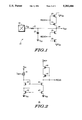
- FIG. 1 illustrates in schematic form a voltage limiter circuit in accordance with the present invention.
- FIG. 2 illustrates in schematic form a bias voltage generator circuit providing a first bias voltage to the voltage limiter circuit of FIG. 1.
- FIG. 3 illustrates in schematic form a bias voltage generator circuit providing a second bias voltage to the voltage limiter circuit of FIG. 1.
- FIG. 4 illustrates in graphical form the transfer function of the voltage limiter circuit of FIG. 1.
- FIG. 5 illustrates in schematic form a single-ended to differential converter using a voltage limiter in accordance with the present invention.
- FIG. 1 illustrates in schematic form a voltage limiter circuit 20 in accordance with the present invention.
- Voltage limiter circuit 20 includes generally a resistor 21, a capacitor 22, P-channel transistors 23 and 24, and N-channel transistors 25 and 26.
- FIG. 1 also illustrates a bonding pad 30 for receiving an input signal.
- Resistor 21 has a first terminal connected to bonding pad 30, and a second terminal connected to a node 28 and providing an output voltage of the voltage limiter labelled "V OUT ".
- Capacitor 22 has a first terminal connected to the second terminal of resistor 21 at node 28, and a second terminal connected to a power supply voltage terminal labelled "V SS ".
- V SS is a more-negative power supply voltage terminal having a nominal voltage of zero volts.
- Transistor 23 has a source connected to a power supply voltage terminal labelled "V AG ", a gate for receiving a bias signal labelled "PBIAS", and a drain.
- V AG is an analog ground power supply voltage terminal which has a voltage roughly halfway between a more-positive power supply voltage and more-negative power supply voltage, or nominally about 2.25 volts.
- Transistor 24 has a source connected to the drain of transistor 23, a gate for receiving voltage PBIAS, and a drain connected to the second terminal of resistor 21.
- PBIAS is a voltage which is sufficient to bias P-channel transistors 23 and 24 to conduct a reference current. A bulk of each of transistors 23 and 24 is connected to a source thereof.
- Transistor 25 has a source connected to the second terminal of resistor 21 at node 28, a gate for receiving a bias voltage labelled "NBIAS", and a drain.
- Transistor 26 has a source connected to the drain of transistor 25, a gate for receiving voltage NBIAS, a drain connected to V AG , and a bulk connected to V SS .
- NBIAS is a voltage which sufficient to bias N-channel transistors 25 and 26 to conduct a reference current.
- a bulk of each of transistors 25 and 26 is connected to V SS .
- V IN exceeds V AG by more than a first predetermined amount, then node 28 becomes a source to transistor 24, and transistors 23 and 24 begin to conduct.
- the first predetermined amount corresponds to an upper limit of the input voltage range of an analog receiver (not shown) connected to voltage limiter 20.
- PBIAS is a voltage equal to a gate-to-source voltage of P-channel transistors sized similarly to transistors 23 and 24 and conducting a first reference current.
- the first reference current, designated "I REFP ", is equal to the current flowing through resistor 21 and through transistors 24 and 23 to V AG when the voltage at node 28 is at the upper limit.
- V IN is less than V AG by more than a second predetermined amount, then node 28 becomes a source to transistor 25, and transistors 25 and 26 begin to conduct.
- the predetermined amount corresponds to a lower limit of the input voltage range of the analog receiver connected to voltage limiter 20.
- NBIAS is a voltage equal to a gate-to-source voltage of N-channel transistors sized similarly to transistors 25 and 26 and conducting a second reference current.
- the second reference current, designated "I REFN ", is equal to the current flowing from V AG through transistors 26 and 25 and through resistor 21 to V IN when the voltage at node 28 is at the lower limit.
- transistor pairs 23 and 24, and 25 and 26, could each be replaced by a single transistor of the appropriate conductivity type.
- the inclusion of extra cascode transistors 24 and 25 increases the output impedance on node 28, and because subsequent circuitry includes amplifiers using cascode transistors, the inclusion of cascode transistors is preferred.
- FIG. 2 illustrates in schematic form a bias voltage generator circuit 40 providing bias voltage PBIAS to voltage limiter circuit 20 of FIG. 1.
- Bias voltage generator circuit 40 includes generally a current source 41, N-channel transistors 42 and 43, P-channel transistors 44 and 45, and N-channel transistors 46 and 47.
- Current source 41 has a first terminal connected to a power supply voltage terminal labelled "V DD ", and a second terminal.
- V DD is a more-positive power supply voltage terminal with a nominal voltage of 5 volts but which may be as low as approximately 3 volts.
- Transistor 42 has a drain connected to the second terminal of current source 41, a gate connected to the drain thereof, and a source.
- Transistor 43 has a drain connected to the source of transistor 42, a gate connected to the drain thereof, and a source connected to V SS .
- Transistor 44 has a source for receiving a reference voltage labelled "V REFP ", a gate, and a drain.
- V REFP is a reference voltage having a nominal value of apporximately 3.35 volts.
- Transistor 45 has a source connected to the drain of transistor 44, a gate, and a drain for providing bias voltage PBIAS and connected to the gates of transistors 44 and 45.
- Transistor 46 has a drain connected to the drain of transistor 45, a gate connected to the drain of transistor 42, and a source.
- Transistor 47 has a drain connected to the source of transistor 46, a gate connected to the drain of transistor 43, and a source connected to V SS .
- Transistors 42, 43, 46, and 47 collectively form a cascode current mirror, which mirrors a current equal to I REFP from the drain of transistor 45.
- transistors 44 and 45 have the same gate width-to-length ratio as transistors 23 and 24 of FIG. 1. In other embodiments, transistors 44 and 45 could be ratioed to transistors 23 and 24, but I REFP must be similarly ratioed to provide the same current density through transistors 23 and 24. If V MAX is equal to the maximum value expected for V IN , V LIMITU is equal to the value of V IN which causes transistors 23 and 24 to conduct, and R 21 is equal to the resistance of resistor 21, then
- V MAX is equal to approximately 5.0 volts
- V LIMITU is equal to approximately 2.9 volts.
- FIG. 3 illustrates in schematic form a bias voltage generator circuit 50 providing bias voltage NBIAS to voltage limiter circuit 20 of FIG. 1.
- Bias voltage generator circuit 50 includes generally P-channel transistors 51 and 52, a current source 53, P-channel transistors 54 and 55, and N-channel transistors 56 and 57.
- Transistor 51 has a source connected to V DD , a gate, and a drain connected to the gate thereof.
- Transistor 52 has a source connected to the drain of transistor 51, a gate, and a drain connected to the gate thereof.
- Current source 53 has a first terminal connected to the drain of transistor 52, and a second terminal connected to V SS .
- Transistor 54 has a source connected to V DD , a gate connected to the drain of transistor 51, and a drain.
- Transistor 55 has a source connected to the drain of transistor 54, a gate connected to the drain of transistor 52, and a drain for providing voltage NBIAS.
- Transistor 56 has a drain connected to the drain of transistor 55, a gate connected to the drain thereof, and a source.
- Transistor 57 has a drain connected to the source of transistor 56, a gate connected to the drain of transistor 56, and a source for receiving a reference voltage labelled "V REFN ".
- V REFN is a reference voltage having a nominal value of approximately 1.15 volts.
- transistors 51, 52, 54, and 55 collectively form a cascode current mirror, which mirrors a current equal to I REFN into the drain of transistor 56.
- transistors 56 and 57 have the same gate width-to-length ratio as transistors 25 and 26 of FIG. 1. In other embodiments, transistors 56 and 57 could be ratioed to transistors 25 and 26, but I REFN must be similarly ratioed to provide the same current density through transistors 25 and 26. If V MIN is equal to the minimum value expected for V IN , V LIMITL is equal to the value of V IN which causes transistors 23 and 24 to conduct, and R 21 is equal to the resistance of resistor 21, then
- V LIMITL is equal to approximately 1.4 volts
- V MIN is equal to approximately 0 volts.
- FIG. 4 illustrates in graphical form the transfer function of voltage limiter circuit 20 of FIG. 1.
- the horizontal axis represents V IN
- the vertical axis represents V OUT .
- transistors 25 and 26 are conductive and maintain V OUT within the dynamic range of a subsequent amplifier.
- the transfer function is linear because neither transistor pair 23 and 24, nor transistor pair 25 and 26, are conductive.
- transistors 23 and 24 are conductive to maintain V OUT within the dynamic range of the subsequent amplifier.
- V OUT is maintained between 1.0 and 3.5 volts as V IN varies between 0 and 5 volts.
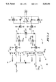
- FIG. 5 illustrates in schematic form a single-ended to differential converter 60 using a voltage limiter in accordance with the present invention.
- Single-ended to differential converter 60 includes generally a voltage limiter 80 and an amplifier 100.
- Voltage limiter 80 includes generally resistors 81 and 82, a capacitor 83, P-channel transistors 84 and 85, N-channel transistors 86 and 87, P-channel transistors 94 and 95, and N-channel transistors 96 and 97.
- Amplifier 100 includes transmission gates 101-104, capacitors 105 and 106, transmission gates 107-109, a fully-differential amplifier 110, a transmission gate 111, capacitors 112 and 113, and a transmission gate 114.
- Resistor 81 has a first terminal for receiving input voltage V IN , and a second terminal.
- Resistor 82 has a first terminal connected to V AG , and a second terminal.
- Capacitor 83 has a first terminal connected to the second terminal of resistor 81, and a second terminal connected to the second terminal of resistor 82.
- Transistor 84 has a source connected to V AG , a gate for receiving voltage PBIAS, and a drain.
- Transistor 85 has a source connected to the drain of transistor 84, a gate for receiving voltage PBIAS, and a drain connected to the second terminal of resistor 81.
- Transistor 86 has a source connected to the second terminal of resistor 81, a gate for receiving voltage NBIAS, and a drain.
- Transistor 87 has a source connected to the drain of transistor 86, a gate for receiving voltage NBIAS, and a drain connected to V AG .
- Transistor 94 has a source connected to V AG , a gate for receiving voltage PBIAS, and a drain.
- Transistor 95 has a source connected to the drain of transistor 94, a gate for receiving voltage PBIAS, and a drain connected to the second terminal of resistor 82.
- Transistor 96 has a source connected to the second terminal of resistor 82, a gate for receiving voltage NBIAS, and a drain.
- Transistor 97 has a source connected to the drain of transistor 96, a gate for receiving voltage NBIAS, and a drain connected to V AG .
- resistor 81, capacitor 83, and transistors 84-87 form a first voltage limiter 90.
- Resistor 82, capacitor 83, and transistors 94-97 form a second voltage limiter 92.
- Capacitor 83 is shared between voltage limiters 90 and 92.
- each transmission gate has first and second terminals and is operative in response to one of two clock signals.
- Transmission gates operative during a clock signal labelled “ ⁇ 0" have a positive control terminal for receiving signal ⁇ 0 and a negative control terminal for receiving a complement of signal ⁇ 0 labelled " ⁇ 0".
- Transmission gates operative during a clock signal labelled “ ⁇ 1" have a positive control terminal for receiving signal ⁇ 1 and a negative control terminal for receiving a complement of signal ⁇ 1 labelled " ⁇ 1".
- Transmission gate 101 has a first terminal connected to the second terminal of resistor 81, and a second terminal, and is operative during ⁇ 1.
- Transmission gate 102 has a first terminal connected to the second terminal of resistor 82, and a second terminal, and is operative during ⁇ 1.
- Transmission gate 103 has a first terminal connected to the second terminal of transmission gate 101, and a second terminal connected to V AG , and is operative during ⁇ 0.
- Transmission gate 104 has a first terminal connected to the second terminal of transmission gate 102, and a second terminal connected to V AG , and is operative during ⁇ 0.
- Capacitor 105 has a first terminal connected to the second terminal of transmission gate 101, and a second terminal.
- Capacitor 106 has a first terminal connected to the second terminal of transmission gate 102, and a second terminal.
- Transmission gate 107 has a first terminal connected to the second terminal of capacitor 105, and a second terminal connected to the second terminal of capacitor 106, and is operative during ⁇ 1.
- Transmission gate 108 has a first terminal connected to the second terminal of capacitor 105, and a second terminal, and is operative during ⁇ 0.
- Transmission gate 109 has a first terminal connected to the second terminal of capacitor 106, and a second terminal, and is operative during ⁇ 0.
- Amplifier 110 has a positive input terminal connected to the second terminal of transmission gate 108, a negative input terminal connected to the second terminal of transmission gate 109, a negative output terminal for providing a positive output signal of single-ended to differential converter 60 labelled "V OUT+ ", and a positive output terminal for providing a negative output signal of single-ended to differential converter 60 labelled "V OUT- ".
- amplifier 110 is fully symmetrical and the designation of positive and negative input and output terminals is interchangeable.
- Transmission gate 111 has a first terminal connected to the second terminal of transmission gate 108, and a second terminal connected to the negative output terminal of amplifier 110, and is operative during ⁇ 1.
- Capacitor 112 has a first terminal connected to the positive input terminal of amplifier 110, and a second terminal connected to the negative output terminal of amplifier 110.
- Capacitor 113 has a first terminal connected to the negative input terminal of amplifier 110, and a second terminal connected to the positive output terminal of amplifier 110.
- Transmission gate 114 has a first terminal connected to the second terminal of transmission gate 109, and a second terminal connected to the positive output terminal of amplifier 110, and is operative during ⁇ 1.
- Voltage limiter 80 and amplifier 100 together increase the system power supply rejection ratio (PSRR) by creating a pseudo-balanced voltage limiter on a single-ended to differential converter.
- Voltage limiter 92 creates a dummy balanced node on node 98 that has equal noise impairments to those on node 88.
- Amplifier 100 thus sees any power supply noise as a common-mode noise component between nodes 88 and 98; by rejecting the common-mode component, amplifier 100 increases system noise rejection.
- single-ended to differential converter 60 improves the system PSRR over known single-ended to differential converters which are subject to large power supply noise transients.
- a voltage limiter may omit the cascode transistors in other embodiments.
- voltage limiters 90 and 92 may be used with other amplifier types besides switched-capacitor amplifier 100 to form a single-ended to differential converter. Accordingly, it is intended by the appended claims to cover all modifications of the invention which fall within the true spirit and scope of the invention.
Abstract
Description
I.sub.REFP =(V.sub.MAX -V.sub.LIMITU)/R.sub.21 [ 1].
I.sub.REFN =(V.sub.LIMITL -V.sub.MIN)/R.sub.21 [ 2].
Claims (17)
Priority Applications (1)
| Application Number | Priority Date | Filing Date | Title |
|---|---|---|---|
| US07/959,578 US5283484A (en) | 1992-10-13 | 1992-10-13 | Voltage limiter and single-ended to differential converter using same |
Applications Claiming Priority (1)
| Application Number | Priority Date | Filing Date | Title |
|---|---|---|---|
| US07/959,578 US5283484A (en) | 1992-10-13 | 1992-10-13 | Voltage limiter and single-ended to differential converter using same |
Publications (1)
| Publication Number | Publication Date |
|---|---|
| US5283484A true US5283484A (en) | 1994-02-01 |
Family
ID=25502170
Family Applications (1)
| Application Number | Title | Priority Date | Filing Date |
|---|---|---|---|
| US07/959,578 Expired - Lifetime US5283484A (en) | 1992-10-13 | 1992-10-13 | Voltage limiter and single-ended to differential converter using same |
Country Status (1)
| Country | Link |
|---|---|
| US (1) | US5283484A (en) |
Cited By (19)
| Publication number | Priority date | Publication date | Assignee | Title |
|---|---|---|---|---|
| US5404050A (en) * | 1992-12-11 | 1995-04-04 | U.S. Philips Corporation | Single-to-differential converter |
| US5666069A (en) * | 1995-12-22 | 1997-09-09 | Cypress Semiconductor Corp. | Data output stage incorporating an inverting operational amplifier |
| US5691654A (en) * | 1995-12-14 | 1997-11-25 | Cypress Semiconductor Corp. | Voltage level translator circuit |
| US5721504A (en) * | 1995-04-21 | 1998-02-24 | Mitsubishi Denki Kabushiki Kaisha | Clamping semiconductor circuit |
| US5945878A (en) * | 1998-02-17 | 1999-08-31 | Motorola, Inc. | Single-ended to differential converter |
| US6608527B2 (en) | 1999-10-21 | 2003-08-19 | Broadcom Corporation | Adaptive radio transceiver with low noise amplification |
| US20030189448A1 (en) * | 2002-04-08 | 2003-10-09 | Silicon Video, Inc. | MOSFET inverter with controlled slopes and a method of making |
| US6738601B1 (en) * | 1999-10-21 | 2004-05-18 | Broadcom Corporation | Adaptive radio transceiver with floating MOSFET capacitors |
| US20050181754A1 (en) * | 1999-10-21 | 2005-08-18 | Stephen Wu | Adaptive radio transceiver with calibration |
| US20050200395A1 (en) * | 2004-03-10 | 2005-09-15 | Pham Giao M. | Method and apparatus for robust mode selection with low power consumption |
| US20060055577A1 (en) * | 2004-08-31 | 2006-03-16 | Christian Boemler | Minimized differential SAR-type column-wide ADC for CMOS image sensors |
| US20070152753A1 (en) * | 2006-01-05 | 2007-07-05 | Texas Instruments Incorporated | System and method for clamping a differential amplifier |
| US20080143385A1 (en) * | 2003-05-22 | 2008-06-19 | Sherif Hanna | High-speed differential logic to CMOS translator architecture with low data-dependent jitter and duty cycle distortion |
| US7548726B1 (en) * | 1999-10-21 | 2009-06-16 | Broadcom Corporation | Adaptive radio transceiver with a bandpass filter |
| US9438262B1 (en) * | 2015-06-22 | 2016-09-06 | Freescale Semiconductor, Inc. | Method for testing differential analog-to-digital converter and system therefor |
| GB2547799A (en) * | 2016-02-26 | 2017-08-30 | Cirrus Logic Int Semiconductor Ltd | Clamping audio signal paths |
| GB2547730A (en) * | 2016-02-26 | 2017-08-30 | Cirrus Logic Int Semiconductor Ltd | Clamping audio signal paths |
| TWI624746B (en) * | 2015-11-24 | 2018-05-21 | 美商豪威科技股份有限公司 | Interface circuit for transmitting signals and method of generating output differential signals |
| CN109002739A (en) * | 2017-06-07 | 2018-12-14 | 北京普源精电科技有限公司 | A kind of absolute value circuit |
Citations (4)
| Publication number | Priority date | Publication date | Assignee | Title |
|---|---|---|---|---|
| US4697152A (en) * | 1986-04-11 | 1987-09-29 | Motorola, Inc. | Fully differential switched capacitor amplifier having autozeroed common-mode feedback |
| US4849708A (en) * | 1988-06-30 | 1989-07-18 | Advanced Miere Devices, Inc. | Fully differential non-linear amplifier |
| US4996504A (en) * | 1988-09-30 | 1991-02-26 | Siemens Aktiengesellschaft | Monolithically integratable microwave attenuation element |
| US5155396A (en) * | 1989-10-03 | 1992-10-13 | Marelli Autronica Spa | Integrated interface circuit for processing the signal supplied by a capacitive sensor |
-
1992
- 1992-10-13 US US07/959,578 patent/US5283484A/en not_active Expired - Lifetime
Patent Citations (4)
| Publication number | Priority date | Publication date | Assignee | Title |
|---|---|---|---|---|
| US4697152A (en) * | 1986-04-11 | 1987-09-29 | Motorola, Inc. | Fully differential switched capacitor amplifier having autozeroed common-mode feedback |
| US4849708A (en) * | 1988-06-30 | 1989-07-18 | Advanced Miere Devices, Inc. | Fully differential non-linear amplifier |
| US4996504A (en) * | 1988-09-30 | 1991-02-26 | Siemens Aktiengesellschaft | Monolithically integratable microwave attenuation element |
| US5155396A (en) * | 1989-10-03 | 1992-10-13 | Marelli Autronica Spa | Integrated interface circuit for processing the signal supplied by a capacitive sensor |
Cited By (49)
| Publication number | Priority date | Publication date | Assignee | Title |
|---|---|---|---|---|
| US5404050A (en) * | 1992-12-11 | 1995-04-04 | U.S. Philips Corporation | Single-to-differential converter |
| US5721504A (en) * | 1995-04-21 | 1998-02-24 | Mitsubishi Denki Kabushiki Kaisha | Clamping semiconductor circuit |
| US5691654A (en) * | 1995-12-14 | 1997-11-25 | Cypress Semiconductor Corp. | Voltage level translator circuit |
| US5666069A (en) * | 1995-12-22 | 1997-09-09 | Cypress Semiconductor Corp. | Data output stage incorporating an inverting operational amplifier |
| US5945878A (en) * | 1998-02-17 | 1999-08-31 | Motorola, Inc. | Single-ended to differential converter |
| US7756472B2 (en) | 1999-10-21 | 2010-07-13 | Broadcom Corporation | Adaptive radio transceiver with filtering |
| US20040195917A1 (en) * | 1999-10-21 | 2004-10-07 | Ahmadreza Rofougaran | Adaptive radio transceiver with floating MOSFET capacitors |
| US6738601B1 (en) * | 1999-10-21 | 2004-05-18 | Broadcom Corporation | Adaptive radio transceiver with floating MOSFET capacitors |
| US7389087B2 (en) | 1999-10-21 | 2008-06-17 | Broadcom Corporation | Adaptive radio transceiver with filtering |
| US6920311B2 (en) | 1999-10-21 | 2005-07-19 | Broadcom Corporation | Adaptive radio transceiver with floating MOSFET capacitors |
| US20050181754A1 (en) * | 1999-10-21 | 2005-08-18 | Stephen Wu | Adaptive radio transceiver with calibration |
| US8116690B2 (en) | 1999-10-21 | 2012-02-14 | Broadcom Corporation | Adaptive radio transceiver with floating mosfet capacitors |
| US6968167B1 (en) * | 1999-10-21 | 2005-11-22 | Broadcom Corporation | Adaptive radio transceiver with calibration |
| US6987966B1 (en) * | 1999-10-21 | 2006-01-17 | Broadcom Corporation | Adaptive radio transceiver with polyphase calibration |
| US8041294B2 (en) | 1999-10-21 | 2011-10-18 | Broadcom Corporation | Adaptive radio transceiver |
| US6608527B2 (en) | 1999-10-21 | 2003-08-19 | Broadcom Corporation | Adaptive radio transceiver with low noise amplification |
| US7139540B2 (en) | 1999-10-21 | 2006-11-21 | Broadcom Corporation | Adaptive radio transceiver with calibration |
| US20090286487A1 (en) * | 1999-10-21 | 2009-11-19 | Broadcom Corporation | Adaptive radio transceiver |
| US7548726B1 (en) * | 1999-10-21 | 2009-06-16 | Broadcom Corporation | Adaptive radio transceiver with a bandpass filter |
| US7233772B1 (en) * | 1999-10-21 | 2007-06-19 | Broadcom Corporation | Adaptive radio transceiver with filtering |
| US20080290966A1 (en) * | 1999-10-21 | 2008-11-27 | Broadcom Corporation | Adaptive radio transceiver with filtering |
| US20080191313A1 (en) * | 1999-10-21 | 2008-08-14 | Broadcom Corporation | Adaptive radio transceiver with floating mosfet capacitors |
| US20070285154A1 (en) * | 1999-10-21 | 2007-12-13 | Broadcom Corporation | Adaptive radio transceiver with filtering |
| US7356310B2 (en) | 1999-10-21 | 2008-04-08 | Broadcom Corporation | Adaptive radio transceiver with floating MOSFET capacitors |
| US20030189448A1 (en) * | 2002-04-08 | 2003-10-09 | Silicon Video, Inc. | MOSFET inverter with controlled slopes and a method of making |
| US20080143385A1 (en) * | 2003-05-22 | 2008-06-19 | Sherif Hanna | High-speed differential logic to CMOS translator architecture with low data-dependent jitter and duty cycle distortion |
| US7777521B2 (en) | 2003-05-22 | 2010-08-17 | Cypress Semiconductor Corporation | Method and circuitry to translate a differential logic signal to a CMOS logic signal |
| US20100109741A1 (en) * | 2004-03-10 | 2010-05-06 | Power Integrations, Inc. | Method and apparatus for robust mode selection with low power consumption |
| US20070188213A1 (en) * | 2004-03-10 | 2007-08-16 | Pham Giao M | Method and apparatus for robust mode selection with low power consumption |
| US7212058B2 (en) * | 2004-03-10 | 2007-05-01 | Power Integrations, Inc. | Method and apparatus for robust mode selection with low power consumption |
| US7667518B2 (en) | 2004-03-10 | 2010-02-23 | Power Integrations, Inc. | Method and apparatus for robust mode selection with low power consumption |
| US20050200395A1 (en) * | 2004-03-10 | 2005-09-15 | Pham Giao M. | Method and apparatus for robust mode selection with low power consumption |
| US7936202B2 (en) | 2004-03-10 | 2011-05-03 | Power Integrations, Inc. | Method and apparatus for robust mode selection with low power consumption |
| US20080258954A1 (en) * | 2004-08-31 | 2008-10-23 | Christian Boemler | Method of controlling digital-to-analog conversion |
| US20060055577A1 (en) * | 2004-08-31 | 2006-03-16 | Christian Boemler | Minimized differential SAR-type column-wide ADC for CMOS image sensors |
| US7567196B2 (en) | 2004-08-31 | 2009-07-28 | Aptina Imaging Corporation | Method of controlling digital-to-analog conversion |
| US7151475B2 (en) * | 2004-08-31 | 2006-12-19 | Micron Technology, Inc. | Minimized differential SAR-type column-wide ADC for CMOS image sensors |
| US20060208936A1 (en) * | 2004-08-31 | 2006-09-21 | Christian Boemler | Minimized differential SAR-type column-wide ADC for CMOS image sensors |
| US7385547B2 (en) | 2004-08-31 | 2008-06-10 | Micron Technology, Inc. | Minimized differential SAR-type column-wide ADC for CMOS image sensors |
| US20070152753A1 (en) * | 2006-01-05 | 2007-07-05 | Texas Instruments Incorporated | System and method for clamping a differential amplifier |
| US7368991B2 (en) * | 2006-01-05 | 2008-05-06 | Texas Instruments Incorporated | System and method for clamping a differential amplifier |
| US9438262B1 (en) * | 2015-06-22 | 2016-09-06 | Freescale Semiconductor, Inc. | Method for testing differential analog-to-digital converter and system therefor |
| TWI624746B (en) * | 2015-11-24 | 2018-05-21 | 美商豪威科技股份有限公司 | Interface circuit for transmitting signals and method of generating output differential signals |
| GB2547799A (en) * | 2016-02-26 | 2017-08-30 | Cirrus Logic Int Semiconductor Ltd | Clamping audio signal paths |
| GB2547730A (en) * | 2016-02-26 | 2017-08-30 | Cirrus Logic Int Semiconductor Ltd | Clamping audio signal paths |
| GB2547730B (en) * | 2016-02-26 | 2018-08-01 | Cirrus Logic Int Semiconductor Ltd | Clamping audio signal paths |
| US10142721B2 (en) | 2016-02-26 | 2018-11-27 | Cirrus Logic, Inc. | Clamping audio signal paths |
| CN109002739B (en) * | 2017-06-07 | 2020-03-17 | 北京普源精电科技有限公司 | Absolute value circuit |
| CN109002739A (en) * | 2017-06-07 | 2018-12-14 | 北京普源精电科技有限公司 | A kind of absolute value circuit |
Similar Documents
| Publication | Publication Date | Title |
|---|---|---|
| US5283484A (en) | Voltage limiter and single-ended to differential converter using same | |
| EP0766381B1 (en) | Improved single-ended to differential converter with relaxed common-mode input requirements | |
| KR100204180B1 (en) | Monolithic integrated differential amplifier | |
| EP0554743B1 (en) | Differential amplifier with common-mode stability enhancement | |
| US7474151B2 (en) | Active load with adjustable common-mode level | |
| US5568089A (en) | Fully differential amplifier including common mode feedback circuit | |
| US5343160A (en) | Fully balanced transimpedance amplifier with low noise and wide bandwidth | |
| US5115151A (en) | Triple comparator circuit | |
| US5917368A (en) | Voltage-to-current converter | |
| US4897612A (en) | Operational transconductance amplifier with improved current source capability | |
| US5146179A (en) | Fully differential operational amplifier having frequency dependent impedance division | |
| US4069431A (en) | Amplifier circuit | |
| EP0832515B1 (en) | A low-voltage rail-to-rail operational amplifier | |
| US6958644B2 (en) | Active filter circuit with dynamically modifiable gain | |
| US4731590A (en) | Circuits with multiple controlled gain elements | |
| EP0240114B1 (en) | A comparator for comparing differential input signals and method therefor | |
| US4460874A (en) | Three-terminal operational amplifier/comparator with offset compensation | |
| US6642788B1 (en) | Differential cascode amplifier | |
| JPH0730340A (en) | Differential input stage with improved common mode rejection | |
| US6034568A (en) | Broadband dc amplifier technique with very low offset voltage | |
| US4533877A (en) | Telecommunication operational amplifier | |
| US4446444A (en) | CMOS Amplifier | |
| EP0998034B1 (en) | Analog amplifier clipping circuit | |
| US4817208A (en) | Fiber optic receiver | |
| US10122335B2 (en) | Low voltage high speed CMOS line driver without tail current source |
Legal Events
| Date | Code | Title | Description |
|---|---|---|---|
| AS | Assignment |
Owner name: MOTOROLA, INC., ILLINOIS Free format text: ASSIGNMENT OF ASSIGNORS INTEREST.;ASSIGNORS:BREHMER, GEOFFREY E.;CARBERY, JAMES R.;REEL/FRAME:006254/0788 Effective date: 19921008 |
|
| STCF | Information on status: patent grant |
Free format text: PATENTED CASE |
|
| CC | Certificate of correction | ||
| FPAY | Fee payment |
Year of fee payment: 4 |
|
| FPAY | Fee payment |
Year of fee payment: 8 |
|
| AS | Assignment |
Owner name: FREESCALE SEMICONDUCTOR, INC., TEXAS Free format text: ASSIGNMENT OF ASSIGNORS INTEREST;ASSIGNOR:MOTOROLA, INC.;REEL/FRAME:015698/0657 Effective date: 20040404 Owner name: FREESCALE SEMICONDUCTOR, INC.,TEXAS Free format text: ASSIGNMENT OF ASSIGNORS INTEREST;ASSIGNOR:MOTOROLA, INC.;REEL/FRAME:015698/0657 Effective date: 20040404 |
|
| FPAY | Fee payment |
Year of fee payment: 12 |
|
| AS | Assignment |
Owner name: CITIBANK, N.A. AS COLLATERAL AGENT, NEW YORK Free format text: SECURITY AGREEMENT;ASSIGNORS:FREESCALE SEMICONDUCTOR, INC.;FREESCALE ACQUISITION CORPORATION;FREESCALE ACQUISITION HOLDINGS CORP.;AND OTHERS;REEL/FRAME:018855/0129 Effective date: 20061201 Owner name: CITIBANK, N.A. AS COLLATERAL AGENT,NEW YORK Free format text: SECURITY AGREEMENT;ASSIGNORS:FREESCALE SEMICONDUCTOR, INC.;FREESCALE ACQUISITION CORPORATION;FREESCALE ACQUISITION HOLDINGS CORP.;AND OTHERS;REEL/FRAME:018855/0129 Effective date: 20061201 |
|
| AS | Assignment |
Owner name: CITIBANK, N.A., AS COLLATERAL AGENT,NEW YORK Free format text: SECURITY AGREEMENT;ASSIGNOR:FREESCALE SEMICONDUCTOR, INC.;REEL/FRAME:024397/0001 Effective date: 20100413 Owner name: CITIBANK, N.A., AS COLLATERAL AGENT, NEW YORK Free format text: SECURITY AGREEMENT;ASSIGNOR:FREESCALE SEMICONDUCTOR, INC.;REEL/FRAME:024397/0001 Effective date: 20100413 |
|
| AS | Assignment |
Owner name: ZOZO MANAGEMENT, LLC, DELAWARE Free format text: ASSIGNMENT OF ASSIGNORS INTEREST;ASSIGNOR:FREESCALE SEMICONDUCTOR, INC.;REEL/FRAME:034034/0236 Effective date: 20120814 |
|
| AS | Assignment |
Owner name: APPLE INC., CALIFORNIA Free format text: ASSIGNMENT OF ASSIGNORS INTEREST;ASSIGNOR:ZOZO MANAGEMENT, LLC;REEL/FRAME:034732/0019 Effective date: 20141219 |
|
| AS | Assignment |
Owner name: FREESCALE SEMICONDUCTOR, INC., TEXAS Free format text: PATENT RELEASE;ASSIGNOR:CITIBANK, N.A., AS COLLATERAL AGENT;REEL/FRAME:037356/0143 Effective date: 20151207 Owner name: FREESCALE SEMICONDUCTOR, INC., TEXAS Free format text: PATENT RELEASE;ASSIGNOR:CITIBANK, N.A., AS COLLATERAL AGENT;REEL/FRAME:037356/0553 Effective date: 20151207 Owner name: FREESCALE SEMICONDUCTOR, INC., TEXAS Free format text: PATENT RELEASE;ASSIGNOR:CITIBANK, N.A., AS COLLATERAL AGENT;REEL/FRAME:037354/0225 Effective date: 20151207 |