US5293301A - Semiconductor device and lead frame used therein - Google Patents
Semiconductor device and lead frame used therein Download PDFInfo
- Publication number
- US5293301A US5293301A US07/798,736 US79873691A US5293301A US 5293301 A US5293301 A US 5293301A US 79873691 A US79873691 A US 79873691A US 5293301 A US5293301 A US 5293301A
- Authority
- US
- United States
- Prior art keywords
- semiconductor chip
- heat sink
- semiconductor device
- chip
- heat
- Prior art date
- Legal status (The legal status is an assumption and is not a legal conclusion. Google has not performed a legal analysis and makes no representation as to the accuracy of the status listed.)
- Expired - Fee Related
Links
Images


Classifications
-
- H—ELECTRICITY
- H01—ELECTRIC ELEMENTS
- H01L—SEMICONDUCTOR DEVICES NOT COVERED BY CLASS H10
- H01L23/00—Details of semiconductor or other solid state devices
- H01L23/48—Arrangements for conducting electric current to or from the solid state body in operation, e.g. leads, terminal arrangements ; Selection of materials therefor
- H01L23/488—Arrangements for conducting electric current to or from the solid state body in operation, e.g. leads, terminal arrangements ; Selection of materials therefor consisting of soldered or bonded constructions
- H01L23/495—Lead-frames or other flat leads
- H01L23/49541—Geometry of the lead-frame
- H01L23/49558—Insulating layers on lead frames, e.g. bridging members
-
- H—ELECTRICITY
- H01—ELECTRIC ELEMENTS
- H01L—SEMICONDUCTOR DEVICES NOT COVERED BY CLASS H10
- H01L23/00—Details of semiconductor or other solid state devices
- H01L23/34—Arrangements for cooling, heating, ventilating or temperature compensation ; Temperature sensing arrangements
- H01L23/42—Fillings or auxiliary members in containers or encapsulations selected or arranged to facilitate heating or cooling
- H01L23/433—Auxiliary members in containers characterised by their shape, e.g. pistons
- H01L23/4334—Auxiliary members in encapsulations
-
- H—ELECTRICITY
- H01—ELECTRIC ELEMENTS
- H01L—SEMICONDUCTOR DEVICES NOT COVERED BY CLASS H10
- H01L2224/00—Indexing scheme for arrangements for connecting or disconnecting semiconductor or solid-state bodies and methods related thereto as covered by H01L24/00
- H01L2224/01—Means for bonding being attached to, or being formed on, the surface to be connected, e.g. chip-to-package, die-attach, "first-level" interconnects; Manufacturing methods related thereto
- H01L2224/42—Wire connectors; Manufacturing methods related thereto
- H01L2224/44—Structure, shape, material or disposition of the wire connectors prior to the connecting process
- H01L2224/45—Structure, shape, material or disposition of the wire connectors prior to the connecting process of an individual wire connector
- H01L2224/45001—Core members of the connector
- H01L2224/45099—Material
- H01L2224/451—Material with a principal constituent of the material being a metal or a metalloid, e.g. boron (B), silicon (Si), germanium (Ge), arsenic (As), antimony (Sb), tellurium (Te) and polonium (Po), and alloys thereof
-
- H—ELECTRICITY
- H01—ELECTRIC ELEMENTS
- H01L—SEMICONDUCTOR DEVICES NOT COVERED BY CLASS H10
- H01L2224/00—Indexing scheme for arrangements for connecting or disconnecting semiconductor or solid-state bodies and methods related thereto as covered by H01L24/00
- H01L2224/01—Means for bonding being attached to, or being formed on, the surface to be connected, e.g. chip-to-package, die-attach, "first-level" interconnects; Manufacturing methods related thereto
- H01L2224/42—Wire connectors; Manufacturing methods related thereto
- H01L2224/47—Structure, shape, material or disposition of the wire connectors after the connecting process
- H01L2224/48—Structure, shape, material or disposition of the wire connectors after the connecting process of an individual wire connector
- H01L2224/4805—Shape
- H01L2224/4809—Loop shape
- H01L2224/48091—Arched
-
- H—ELECTRICITY
- H01—ELECTRIC ELEMENTS
- H01L—SEMICONDUCTOR DEVICES NOT COVERED BY CLASS H10
- H01L2224/00—Indexing scheme for arrangements for connecting or disconnecting semiconductor or solid-state bodies and methods related thereto as covered by H01L24/00
- H01L2224/01—Means for bonding being attached to, or being formed on, the surface to be connected, e.g. chip-to-package, die-attach, "first-level" interconnects; Manufacturing methods related thereto
- H01L2224/42—Wire connectors; Manufacturing methods related thereto
- H01L2224/47—Structure, shape, material or disposition of the wire connectors after the connecting process
- H01L2224/48—Structure, shape, material or disposition of the wire connectors after the connecting process of an individual wire connector
- H01L2224/481—Disposition
- H01L2224/48151—Connecting between a semiconductor or solid-state body and an item not being a semiconductor or solid-state body, e.g. chip-to-substrate, chip-to-passive
- H01L2224/48221—Connecting between a semiconductor or solid-state body and an item not being a semiconductor or solid-state body, e.g. chip-to-substrate, chip-to-passive the body and the item being stacked
- H01L2224/48245—Connecting between a semiconductor or solid-state body and an item not being a semiconductor or solid-state body, e.g. chip-to-substrate, chip-to-passive the body and the item being stacked the item being metallic
- H01L2224/48247—Connecting between a semiconductor or solid-state body and an item not being a semiconductor or solid-state body, e.g. chip-to-substrate, chip-to-passive the body and the item being stacked the item being metallic connecting the wire to a bond pad of the item
-
- H—ELECTRICITY
- H01—ELECTRIC ELEMENTS
- H01L—SEMICONDUCTOR DEVICES NOT COVERED BY CLASS H10
- H01L2224/00—Indexing scheme for arrangements for connecting or disconnecting semiconductor or solid-state bodies and methods related thereto as covered by H01L24/00
- H01L2224/01—Means for bonding being attached to, or being formed on, the surface to be connected, e.g. chip-to-package, die-attach, "first-level" interconnects; Manufacturing methods related thereto
- H01L2224/42—Wire connectors; Manufacturing methods related thereto
- H01L2224/47—Structure, shape, material or disposition of the wire connectors after the connecting process
- H01L2224/49—Structure, shape, material or disposition of the wire connectors after the connecting process of a plurality of wire connectors
- H01L2224/491—Disposition
- H01L2224/49105—Connecting at different heights
- H01L2224/49109—Connecting at different heights outside the semiconductor or solid-state body
-
- H—ELECTRICITY
- H01—ELECTRIC ELEMENTS
- H01L—SEMICONDUCTOR DEVICES NOT COVERED BY CLASS H10
- H01L2224/00—Indexing scheme for arrangements for connecting or disconnecting semiconductor or solid-state bodies and methods related thereto as covered by H01L24/00
- H01L2224/01—Means for bonding being attached to, or being formed on, the surface to be connected, e.g. chip-to-package, die-attach, "first-level" interconnects; Manufacturing methods related thereto
- H01L2224/50—Tape automated bonding [TAB] connectors, i.e. film carriers; Manufacturing methods related thereto
-
- H—ELECTRICITY
- H01—ELECTRIC ELEMENTS
- H01L—SEMICONDUCTOR DEVICES NOT COVERED BY CLASS H10
- H01L24/00—Arrangements for connecting or disconnecting semiconductor or solid-state bodies; Methods or apparatus related thereto
- H01L24/01—Means for bonding being attached to, or being formed on, the surface to be connected, e.g. chip-to-package, die-attach, "first-level" interconnects; Manufacturing methods related thereto
- H01L24/42—Wire connectors; Manufacturing methods related thereto
- H01L24/44—Structure, shape, material or disposition of the wire connectors prior to the connecting process
- H01L24/45—Structure, shape, material or disposition of the wire connectors prior to the connecting process of an individual wire connector
-
- H—ELECTRICITY
- H01—ELECTRIC ELEMENTS
- H01L—SEMICONDUCTOR DEVICES NOT COVERED BY CLASS H10
- H01L24/00—Arrangements for connecting or disconnecting semiconductor or solid-state bodies; Methods or apparatus related thereto
- H01L24/01—Means for bonding being attached to, or being formed on, the surface to be connected, e.g. chip-to-package, die-attach, "first-level" interconnects; Manufacturing methods related thereto
- H01L24/42—Wire connectors; Manufacturing methods related thereto
- H01L24/47—Structure, shape, material or disposition of the wire connectors after the connecting process
- H01L24/48—Structure, shape, material or disposition of the wire connectors after the connecting process of an individual wire connector
-
- H—ELECTRICITY
- H01—ELECTRIC ELEMENTS
- H01L—SEMICONDUCTOR DEVICES NOT COVERED BY CLASS H10
- H01L24/00—Arrangements for connecting or disconnecting semiconductor or solid-state bodies; Methods or apparatus related thereto
- H01L24/01—Means for bonding being attached to, or being formed on, the surface to be connected, e.g. chip-to-package, die-attach, "first-level" interconnects; Manufacturing methods related thereto
- H01L24/42—Wire connectors; Manufacturing methods related thereto
- H01L24/47—Structure, shape, material or disposition of the wire connectors after the connecting process
- H01L24/49—Structure, shape, material or disposition of the wire connectors after the connecting process of a plurality of wire connectors
-
- H—ELECTRICITY
- H01—ELECTRIC ELEMENTS
- H01L—SEMICONDUCTOR DEVICES NOT COVERED BY CLASS H10
- H01L2924/00—Indexing scheme for arrangements or methods for connecting or disconnecting semiconductor or solid-state bodies as covered by H01L24/00
- H01L2924/0001—Technical content checked by a classifier
- H01L2924/00014—Technical content checked by a classifier the subject-matter covered by the group, the symbol of which is combined with the symbol of this group, being disclosed without further technical details
-
- H—ELECTRICITY
- H01—ELECTRIC ELEMENTS
- H01L—SEMICONDUCTOR DEVICES NOT COVERED BY CLASS H10
- H01L2924/00—Indexing scheme for arrangements or methods for connecting or disconnecting semiconductor or solid-state bodies as covered by H01L24/00
- H01L2924/01—Chemical elements
- H01L2924/01014—Silicon [Si]
-
- H—ELECTRICITY
- H01—ELECTRIC ELEMENTS
- H01L—SEMICONDUCTOR DEVICES NOT COVERED BY CLASS H10
- H01L2924/00—Indexing scheme for arrangements or methods for connecting or disconnecting semiconductor or solid-state bodies as covered by H01L24/00
- H01L2924/01—Chemical elements
- H01L2924/01079—Gold [Au]
-
- H—ELECTRICITY
- H01—ELECTRIC ELEMENTS
- H01L—SEMICONDUCTOR DEVICES NOT COVERED BY CLASS H10
- H01L2924/00—Indexing scheme for arrangements or methods for connecting or disconnecting semiconductor or solid-state bodies as covered by H01L24/00
- H01L2924/013—Alloys
- H01L2924/0132—Binary Alloys
- H01L2924/01322—Eutectic Alloys, i.e. obtained by a liquid transforming into two solid phases
-
- H—ELECTRICITY
- H01—ELECTRIC ELEMENTS
- H01L—SEMICONDUCTOR DEVICES NOT COVERED BY CLASS H10
- H01L2924/00—Indexing scheme for arrangements or methods for connecting or disconnecting semiconductor or solid-state bodies as covered by H01L24/00
- H01L2924/06—Polymers
- H01L2924/078—Adhesive characteristics other than chemical
- H01L2924/07802—Adhesive characteristics other than chemical not being an ohmic electrical conductor
-
- H—ELECTRICITY
- H01—ELECTRIC ELEMENTS
- H01L—SEMICONDUCTOR DEVICES NOT COVERED BY CLASS H10
- H01L2924/00—Indexing scheme for arrangements or methods for connecting or disconnecting semiconductor or solid-state bodies as covered by H01L24/00
- H01L2924/15—Details of package parts other than the semiconductor or other solid state devices to be connected
- H01L2924/181—Encapsulation
Definitions
- This invention relates to a semiconductor device and a lead frame used therein, and more particularly, to a semiconductor device having improved heat radiation characteristics.
- a semiconductor-device having a good heat radiating characteristic is conventionally known, and such a known semiconductor device comprises a semiconductor chip rigidly mounted on a heat sink, so that the heat derived from the semiconductor chip can be discharged via the heat sink and dispersed to the leads or the sealing resin.
- Another conventionally known semiconductor device has a lead frame which comprises two layers, one being a dia-pad having a relatively wide area, so that the heat derived from the semiconductor chip can be discharged via the die-pad.
- An object of the present invention is to provide a semiconductor device and a lead frame used therein and capable of improving the heat radiation characteristic thereof.
- Another object of the present invention is to provide a semiconductor device and a lead frame used therein and capable of overcoming the drawbacks in the prior art, as mentioned above.
- a semiconductor device comprising: a lead frame comprising a heat sink having a peripheral area and a central projected land, said heat sink having a relatively good heat radiating characteristic, and a plurality of inner leads, each having an inner and superimposed on said peripheral area of the heat sink by an electrically insulating material; a semiconductor chip having a chip surface on which a junction pattern is arranged, said semiconductor chip being mounted on said central projected land of the heat sink by an electrically insulating adhesive so that said chip surface faces said projected land; TAB leads for electrically connecting said semiconductor chip to said inner leads; and a sealing resin hermetically sealing at least said semiconductor chip.
- a lead frame to be used for a semiconductor device comprising: a heat sink having a peripheral area and a central projected land on which a semiconductor-chip is mounted, said heat sink having a relatively good heat radiating characteristic; and a plurality of inner leads, each having an inner end superimposed on said peripheral area of the heat sink by an electrically insulating material.
- a semiconductor device comprising: a semiconductor chip having a chip surface on which a junction pattern is arranged; a heat sink made of any suitable material having a coefficient of thermal expansion similar to that of said semiconductor chip, said heat sink being attached to said chip surface of the semiconductor chip by a chip-coated layer; and a sealing resin hermetically sealing at least said semiconductor chip to make a hermetic package.
- a structure for mounting a semiconductor device comprising: a ceramic board made of a material having a coefficient of thermal expansion, a circuit pattern having terminals formed on said ceramic board; said ceramic board being provided integrally with a projected land portion on which a semiconductor chip is to be mounted; a semiconductor chip having a chip surface on which a junction pattern is arranged, said semiconductor chip being mounted on said projected land portion by an electrically insulating adhesivse so that said chip surface faces said projected land; means for electrically connecting said semiconductor chip to said terminals of the circuit pattern on the ceramic board; and a cap means rigidly secured to said ceramic board for enclosing and hermetically sealing said semiconductor chip.
- a structure for mounting a semiconductor device comprising: a ceramic board made of a material having a coefficient of thermal expansion, said ceramic board having one surface provided integrally with a projected land portion on which a semiconductor chip is to be mounted, and holes penetrating said one surface to the other surface thereof; a semiconductor chip having a chip surface on which a junction pattern is arranged, said semiconductor chip being mounted on said projected land portion by an electrically insulating adhesive so that said chip surface faces said projected land; a cap means rigidly secured to said ceramic board for enclosing and hermetically sealing said semiconductor chip; and wires extending from said semiconductor chip through said holes, to be introduced to the other side of the ceramic board.
- FIG. 1 is a plan view of a lead frame according to the present invention
- FIG. 2 is a cross-sectional view of the lead frame shown in FIG. 1;
- FIG. 3 is a cross-sectional view of an embodiment of a semiconductor device according to the present invention.
- FIG. 4 is a cross-sectional view of another embodiment of a semiconductor device of this invention.
- FIG. 5 is a cross-sectional view of still another embodiment of a semiconductor device of this invention.
- FIG. 6 is a cross-sectional view of another embodiment similar to that shown in FIG. 4;
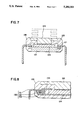
- FIG. 7 is a cross-sectional view of still further embodiment similar to that shown in FIG. 4;
- FIG. 8 is a partial cross-sectional view of a further embodiment of this invention.
- FIG. 9 is a partial cross-sectional view of an embodiment including a ceramic package
- FIG. 10 is a cross-sectional view of an embodiment including a ceramic quad type or metal quad type package
- FIGS. 11 and 12 are cross-sectional views of respective embodiments including radiating fins.
- FIGS. 13 and 14 are cross-sectional views of still other embodiments of a semiconductor device.
- FIG. 1 is a plan view of a lead frame according to the present invention and FIG. 2 is a cross-sectional view of the lead frame shown in FIG. 1, the lead frame 20 includes outer leads 21, inner leads 22, dam bars 23, rails 24, and a heat sink 25.
- the upper periphery of the heat sink 25 is attached, via an electrically insulative adhesive 26, to the lower surfaces of the inner leads 22.
- the upper surface of the heat sink 25 is provided, at an area surrounded by the tips of the inner leads 22, with an upper projected land 27 at substantially the same level as the upper surfaces of the inner leads 22.
- the heat sink 25 can be made of any suitable metal or ceramic having relatively good heat radiating characteristics.
- FIG. 3 is a cross-sectional view of an embodiment of a semiconductor device 30 according to the present invention in which the above-mentioned lead frame 20 is used.
- the semiconductor device 30 comprises the heat sink 25 provided with the upper projected land 27, on which mounted is a semiconductor chip 31 via the insulative adhesive layer 32.
- This semiconductor chip 31 is arranged so that a surface thereof having a junction pattern 37 faces the projected land 27.
- the semiconductor chip 31 is electrically connected to the inner leads 22 via TAB (Tape Automated Bonding) leads 33.
- TAB Pe Automated Bonding
- the heat sink 25 is hermetically sealed with a sealing resin 34, to thus complete this semiconductor device.
- the TAB leads comprise many electrical conductive leads made of, for example, copper foil or layers formed on an insulative carrier, usually called a TAB tape.
- the TAB leads 33 are first electrically connected to the semiconductor chip at one end thereof and electrically connected to the inner leads at the other end thereof, respectively.
- FIG. 4 is a cross-sectional view of another embodiment of a semiconductor device of this invention.
- the semiconductor chip 31 is also provided at the opposite side thereof with another heat sink 35, via an adhesive 36.
- the semiconductor chip 31 and the both heat sinks 25 and 35 are hermetically sealed with a resin so that the lower and upper surfaces of the heat sinks 25 and 35 are exposed to the atmosphere.
- the both heat sinks 25 and 35 may be completely sealed with a resin, or only a part of these heat sinks 25 and 35 ma be exposed to the atmosphere.
- the semiconductor device of this invention As the semiconductor device of this invention is constructed as mentioned above, the heat derived from the surface of the semiconductor chip, on which the junction pattern 37 is arranged and from which a relatively large amount of heat is radiated, is directly discharged via the heat sink 25. Therefore, the semiconductor device of this invention has a good heat radiating cahracteristic and may be constituted as a highly sophisticated device. In the embodiment shown in FIG. 4, in which the heat sink 35 is also provided at the other side of the semiconductor chip, the heat radiating characteristic can be further improved.
- the semiconductor chip 31 since the lead frame 20 is provided with the heat sink 25, the upper surface thereof being provided with the upper projected land 27, the semiconductor chip can be easily secured thereto. Also, since the TAB leads 33 are used, the semiconductor chip 31 may be easily connected to the inner leads 22, even though the semiconductor chip 31 is mounted so that the surface thereof, on which the electrodes are arranged, faces the projected land 27.
- FIG. 5 is a cross-sectional view of a dual-layer type resin sealed semiconductor device of this invention.
- the semiconductor device comprises inner leads 121, outer leads 122, and a die-pad 123.
- the die-pad 123 is relatively large so that the periphery thereof overlaps with the inner leads 121 to improve the heat radiation characteristics and secured to the inner leads 121 via an insulative adhesive.
- a semiconductor chip 124 is rigidly mounted on the die-pad 123 via, for example, an Au-Si eutectic alloy, and the semiconductor chip 124 is electrically connected to the inner leads 121 by bonding wires 125.
- the die-pad 123 also may be used to function as a ground plane. In this case, the die-pad 123 has a terminal connected to one of the inner leads, i.e., a ground line.
- the lead frame 120 is advantageously made of a material having a coefficient of thermal expansion close to that of the semiconductor chip 124, for example, a 42 alloy (Fe-Ni alloy).
- the heat sink 126 is rigidly secured to the surface of the semiconductor chip 124, on which a junction pattern is arranged, via a chip coated layer 127 made of an insulative resin, for example, polyimide.
- the heat sink 126 is advantageously made of a material having a coefficient of thermal expansion close to that of the semiconducter chip 124, for example, Mo, Aln, Sic, Cu-W or the like.
- the heat sink 126 is wider than the semiconductor chip 124, to ensure a sufficient radiation surface.
- the heat sink 126 must be provided with side recesses to maintain escape spaces which prevent the bonding wires 125 from interfering with the heat sink 126. Therefore, in this case, the wires 125 must be first connected to the semiconductor chip 124 by a wire-bonding process, and then the heat sink 126 fixedly secured to the chip surface of the semiconductor chip 124.
- the heat sink 126 has a size and shape such that it does not interfere with the bonding-wires, it is possible to effect the wire-bonding operation after the semiconductor chip 124 is rigidly secured to the heat sink 126.
- the semiconductor chip 124, the die-pad 123, the inner leads 121, the wires 125, and the heat sink 126 are hermetically sealed with a sealing resin 128.
- the heat sink 126 may be completely sealed with the sealing resin 128.
- the heat sink 126 may be sealed with the sealing resin 128 so that the upper surface of the heat sink 126 is exposed at the same level as the outer surface of the sealing resin 128.
- a heat radiation fin 129 is attached to the heat sink 126, as shown by a broken line 129 in FIG. 5.
- the heat derived from the surface of the semiconductor chip 124 can be discharged from the lower surface of the semiconductor chip via the dia-pad 123 and the leads, in the same manner as a semiconductor device known in the prior art. Further, according to the present invention, the heat also can be discharged from the chip surface of the semiconductor chip 124, on which a junction pattern is arranged, and therefore, a large amount of heat is radiated and can be discharged directly via the heat sink 126. Therefore, the semiconductor device of this invention has a good heat radiating characteristic and may be constituted as a highly sophisticated device.
- the coefficient of heat expansion of the sealing resin 128 is generally high, and therefore, it is difficult to match this with the coefficient of heat expansion of the semiconductor chip 124.
- the heat sink 126 and the die-pad 123 are arranged as a sandwich-like structure on the upper and lower sides of the semiconductor chip 124, respectively, the structure of the semiconductor chip 124 is well balanced with respect to the upper and lower direction. Therefore, the sealing resin 128 is not deformed or bent due to a heat shrinkage, and therefore, it is possible to produce a large size semiconductor chip.
- FIG. 6 is a cross-sectional view of an embodiment of a single layer lead frame.
- the die-pad 123 has a small size and is separated from the inner leads 121. Nevertheless, one of the surfaces of the semiconductor chip 124, from which a relatively large amount of heat is radiated, is attached to a heat sink 126, and therefore, the heat radiating characteristics can be improved. Also, in the same manner as the above embodiment, the heat sink 126 and the die-pad 123 are arranged on the upper and lower sides of the semiconductor chip 124, respectively, and the package is not deformed or bent due to heat shrinkage.
- FIG. 7 is a cross-sectional view of an embodiment in which a semiconductor chip 124 is Mounted on a die-pad 123 which also functions as a heat sink, and thus the heat radiating characteristic is improved and the package is not deformed or bent due to heat shrinkage.
- FIG. 8 is a partial cross-sectional view of an embodiment in which a multi-layer lead frame 130 and TAB leads 134 are used.
- the multi-layer lead frame 130 comprises three layers, i.e., a lead frame 131 (signal layer), a power supply plane 132 and a ground plane 133, laminated to each other by insulative sheets.
- the power supply plane 132 and the ground plane 133 have terminals respectively connected to a power supply line and a ground line in the lead frame 131.
- the semiconductor chip 124 is rigidly mounted on the ground plane.
- the heat radiating characteristics can be improved and the package is not deformed or bent due to heat shrinkage, in the same manner as in the above embodiments.
- FIG. 9 is a partial cross-sectional view of an embodiment including a multi-layer ceramic package.
- a semiconductor chip 124 is mounted on a heat sink 123 and a chip surface of the semiconductor chip 124 is attached via a chip coated layer 127 to a cover body 136, which also functions as a heat sink.
- the lower surface of the cover body 136 is provided with a projected land 137 in contact with the chip surface.
- the heat derived from the chip surface of the semiconductor chip 124 can be discharged via the chip coated layer 127 to the housing 136 facing the outside, and therefore, the heat radiating characteristic can be improved.
- a ceramic itself is porous, and therefore, the heat conductivity thereof is not good. According to this embodiment, however, such a heat conductivity of the ceramic package can be improved.
- the lower heat sink may be omitted.
- FIG. 10 shows an embodiment of a semiconductor device including a ceramic quad type or metal quad type package.
- a semiconductor chip 124 is rigidly mounted on a ceramic or metal base 140 having a periphery provided with inner leads 121 of the lead frame 120 attached to the base by a low-melting point glass or resin inner leads.
- the semiconductor chip 224 is connected to the inner leads 121 by bonding wires 125.
- a cover 136 made of ceramic or metal is attached to the periphery of the base 140 so as to cover the semiconductor chip 124 and hold the inner leads 121 via a low-melting point glass or resin.
- the cover 136 is provided at the inside thereof with a projected land 137 attached to the chip surface of the semiconductor chip 124 via the chip coated layer 127.
- the cover 136 also functions as a heat sink.
- the heat radiated from the chip surface of the semiconductor chip 124 can be discharged via the chip coated layer 127 and the projected land 137 to the cover 136 facing the outside, and therefore, the heat radiating characteristics can be improved.
- FIG. 11 is a cross-sectional view of a further embodiment of a semiconductor device.
- a semiconductor chip 124 is rigidly mounted on a cap-shaped base 140 by an adhesive.
- the chip surface of the semiconductor chip 124, on which a junction pattern exists, is attached to a projected land 137 of a cover 136, which also functions as a heat sink, via a chip coated layer 127.
- the periphery of the base 140 is rigidly secured to the periphery of the cover 136, to airtightly enclose the semiconductor chip 124.
- the semiconductor chip 124 has terminals connected to metal wires 125 by wire bonding. The other ends of the wires 125 pass through holes provided in the cover 136 and are introduced to the outside of the cover 136 on which terminals are formed by bumps.
- a heat radiating fin 129 is attached to the outside of the base 140.
- the cover 136 is made of a heat conductive material, such as AlN or the like, which has a coefficient of thermal expansion similar to that of silicon.
- Reference numeral 141 designates a circuit substrate.
- FIG. 12 is a cross-sectional view of an embodiment applied to a PGA type semiconductor device.
- the cover 136 as illustrated in FIG. 11 is formed with a circuit pattern connected to the semiconductor chip 124 by wires 125. External connecting pins 142 are connected to the circuit pattern.
- the heat derived from the chip surface of the semiconductor chip 124, on which a junction pattern exits can be directly discharged via the projected land 137 to the cover 136 facing the outside, and therefore, the heat radiating characteristic can be improved.
- FIGS. 13 and 14 are cross-sectional views of still other embodiments of a semiconductor device.
- the reference numeral 220 designates a circuit board comprising a ceramic substrate made of a heat conductive material, such as AlN or the like, and a circuit pattern formed on the substrate.
- a circuit pattern 222 is formed on the back surface of the ceramic substrate 221.
- the front surface of the ceramic substrate 221, on which a semiconductor device 224 is mounted, is integrally provided with a projected land 225 having a predetermined height.
- the semiconductor device 224 is rigidly secured via an adhesive 230 to a cap 228 made of any suitable metal or the like and having a generally U-shaped cross-section provided with a peripheral flange portion 227 at the open end thereof.
- a heat radiating fin 231 is mounted on the outer side of the cap 228.
- the semiconductor chip 229 has terminals connected to metal wires 233 by wire bonding.
- the semiconductor device 224 is rigidly mounted on the projected land 225 via an insulative adhesion 235, so that the chip surface of the semiconductor chip 229, on which a junction pattern exists, is attached to the projected land 225.
- the cap 228 is rigidly mounted by the peripheral flange portion 227 on the ceramic substrate 221, by a suitable solder 236.
- the wires 233 pass through holes 237 provided in the ceramic substrate 221 and are introduced to the outside of the ceramic substrate 221 to be connected to terminals of the circuit pattern 222 thereon by a solder.
- the heat derived from the chip surface from which a large amount of heat is emitted, can be effectively discharged via the projected land 225 to the ceramic substrate 221, which has a relatively large thermal capacity.
- the heat derived from the back surface of the semiconductor chip 229 also can be effectively discharged via the cap 228 and the heat radiating fin 231.
- this embodiment be applied to a mount of semiconductor device which comprises a high power semiconductor chip, from which a large amount of heat is emitted.
- the ceramic substrate 221 can be made of suitable material, such as AlN or the like, which has a coefficient of thermal expansion similar to that of the semiconductor chip made of silicone, and thus a thermal balance with respect to the semiconductor chip 229 can be attained and a thermal stress at the semiconductor chip 229 also can be reduced.
- suitable material such as AlN or the like
- thermal stress is released by the projected land 225, and therefore, a concentration of thermal stress can be effectively prevented, compared with a device, for example, a chip-on-board type semiconductor device, in which a semiconductor chip is directly mounted on a circuit board.
- external connecting wires 233 of the semiconductor chip 229 are connected to the ceramic substrate 221, and thus a direct electrical connection between the semiconductor chip 229 and the circuit pattern of the substrate 221 can be attained. Therefore, an mounting area or space can be reduced, compared with a Galwing type semiconductor device, and therefore, a highly sophisticated semiconductor device can be obtained.
- FIG. 14 shows another embodiment of semiconductor device, in which the ceramic substrate 221 is provided with terminals connected to the circuit patterns 222 by via 240.
- circuit pattern 222 is formed on the back surface of the ceramic substrate 221 in this embodiment, such a circuit pattern 222 can be formed on the front surface thereof, on which a semiconductor device 240 is mounted (not illustrated).
Abstract
Description
Claims (4)
Applications Claiming Priority (6)
| Application Number | Priority Date | Filing Date | Title |
|---|---|---|---|
| JP2340500A JPH04207058A (en) | 1990-11-30 | 1990-11-30 | Structure for packaging semiconductor device |
| JP2340496A JPH04207061A (en) | 1990-11-30 | 1990-11-30 | Semiconductor device |
| JP2-340501 | 1990-11-30 | ||
| JP2340501A JP2962575B2 (en) | 1990-11-30 | 1990-11-30 | Semiconductor device |
| JP2-340500 | 1990-11-30 | ||
| JP2-340496 | 1990-11-30 |
Publications (1)
| Publication Number | Publication Date |
|---|---|
| US5293301A true US5293301A (en) | 1994-03-08 |
Family
ID=27340965
Family Applications (1)
| Application Number | Title | Priority Date | Filing Date |
|---|---|---|---|
| US07/798,736 Expired - Fee Related US5293301A (en) | 1990-11-30 | 1991-11-27 | Semiconductor device and lead frame used therein |
Country Status (2)
| Country | Link |
|---|---|
| US (1) | US5293301A (en) |
| EP (1) | EP0488783A3 (en) |
Cited By (33)
| Publication number | Priority date | Publication date | Assignee | Title |
|---|---|---|---|---|
| US5461201A (en) * | 1993-01-22 | 1995-10-24 | Siemens Aktiengesellschaft | Insulating part with integral cooling element |
| US5471011A (en) * | 1994-05-26 | 1995-11-28 | Ak Technology, Inc. | Homogeneous thermoplastic semi-conductor chip carrier package |
| US5617294A (en) * | 1995-09-29 | 1997-04-01 | Intel Corporation | Apparatus for removing heat from an integrated circuit package that is attached to a printed circuit board |
| US5650915A (en) * | 1994-05-25 | 1997-07-22 | Texas Instruments Incorporated | Thermally enhanced molded cavity package having a parallel lid |
| US5650593A (en) * | 1994-05-26 | 1997-07-22 | Amkor Electronics, Inc. | Thermally enhanced chip carrier package |
| US5969413A (en) * | 1994-09-29 | 1999-10-19 | Kabushiki Kaishi Toshiba | Semiconductor device having a tab chip on a tape carrier with lead wirings provided on the tape carrier used as external leads |
| US6259603B1 (en) * | 1997-11-13 | 2001-07-10 | Robert Bosch Gmbh | Electronic control unit |
| US6354485B1 (en) * | 1996-10-24 | 2002-03-12 | Tessera, Inc. | Thermally enhanced packaged semiconductor assemblies |
| US20020109211A1 (en) * | 2001-02-09 | 2002-08-15 | Mitsubishi Denki Kabushiki Kaisha | Semiconductor device and method of manufacturing same |
| US20020117764A1 (en) * | 2001-02-28 | 2002-08-29 | Siliconware Precision Industries Co., Ltd. | Lead-on-chip type of semiconductor package with embedded heat sink |
| US20030022464A1 (en) * | 2001-07-26 | 2003-01-30 | Naohiko Hirano | Transfer-molded power device and method for manufacturing transfer-molded power device |
| US20030209783A1 (en) * | 2002-02-18 | 2003-11-13 | Stmicroelectronics S.R.I. | Assembly structure for electronic power integrated circuit formed on a semiconductor die and corresponding manufacturing process |
| US6703707B1 (en) * | 1999-11-24 | 2004-03-09 | Denso Corporation | Semiconductor device having radiation structure |
| US6716676B2 (en) * | 2001-06-04 | 2004-04-06 | Siliconware Precision Industries Co., Ltd. | Thermally-enhanced stacked-die ball grid array semiconductor package and method of fabricating the same |
| US20040119158A1 (en) * | 2002-12-19 | 2004-06-24 | Tatt Koay Hean | Thermally enhanced package for an integrated circuit |
| US20040124508A1 (en) * | 2002-11-27 | 2004-07-01 | United Test And Assembly Test Center Ltd. | High performance chip scale leadframe package and method of manufacturing the package |
| US6784022B2 (en) * | 1998-09-02 | 2004-08-31 | Texas Instruments Incorporated | Method of dicing a semiconductor wafer and heat sink into individual semiconductor integrated circuits |
| US20040180474A1 (en) * | 2003-03-10 | 2004-09-16 | Oman Todd P. | Electronic assembly having electrically-isolated heat-conductive structure and method therefor |
| US20050168304A1 (en) * | 2004-01-29 | 2005-08-04 | Takeshi Yamaguchi | Signal line circuit device |
| DE102004019442A1 (en) * | 2004-04-19 | 2005-10-06 | Siemens Ag | Method for manufacturing low power converters, involves applying layer of electrically insulating material to substrate and component |
| DE102004019435A1 (en) * | 2004-04-19 | 2005-11-03 | Siemens Ag | On a cooling fin arranged component |
| EP1596434A1 (en) * | 2003-09-04 | 2005-11-16 | Matsushita Electric Industrial Co., Ltd. | Semiconductor device |
| US20060103008A1 (en) * | 2004-11-15 | 2006-05-18 | Stats Chippac Ltd. | Hyper thermally enhanced semiconductor package system |
| US20060131735A1 (en) * | 2004-11-15 | 2006-06-22 | Stats Chippac Ltd. | Hyper thermally enhanced semiconductor package system |
| US20070085177A1 (en) * | 2005-10-14 | 2007-04-19 | Stmicroelectronics Asia Pacific Pte Ltd | Semiconductor package with position member |
| CN1332442C (en) * | 2003-11-21 | 2007-08-15 | 株式会社电装 | Semiconductor device with a pair of radiating fan |
| US20070241450A1 (en) * | 2006-04-17 | 2007-10-18 | Mitsubishi Electric Corporation | Semiconductor device |
| US20100019380A1 (en) * | 2008-07-24 | 2010-01-28 | Yi Min Lin | Integrated circuit with micro-pores ceramic heat sink |
| EP2164100A3 (en) * | 2008-09-15 | 2010-11-24 | Delphi Technologies, Inc. | Leaded semiconductor power module with direct bonding and double sided cooling |
| US8304871B2 (en) * | 2011-04-05 | 2012-11-06 | Texas Instruments Incorporated | Exposed die package for direct surface mounting |
| US9953903B2 (en) | 2015-07-22 | 2018-04-24 | Nxp B.V. | Heatsink very-thin quad flat no-leads (HVQFN) package |
| US20220173019A1 (en) * | 2020-12-02 | 2022-06-02 | Shinko Electric Industries Co., Ltd. | Lead frame, semiconductor device, and manufacturing method of lead frame |
| US11380599B2 (en) * | 2019-06-24 | 2022-07-05 | Fuji Electric Co., Ltd. | Semiconductor module, vehicle, and method of manufacturing semiconductor module |
Families Citing this family (10)
| Publication number | Priority date | Publication date | Assignee | Title |
|---|---|---|---|---|
| JP3322429B2 (en) * | 1992-06-04 | 2002-09-09 | 新光電気工業株式会社 | Semiconductor device |
| JPH06204285A (en) * | 1992-12-28 | 1994-07-22 | Toshiba Corp | Semiconductor device and manufacture thereof |
| US5394607A (en) * | 1993-05-20 | 1995-03-07 | Texas Instruments Incorporated | Method of providing low cost heat sink |
| FR2740609B1 (en) * | 1995-10-30 | 1998-02-13 | Sgs Thomson Microelectronics | INTEGRATED CIRCUIT BOX WITH BALL MATRIX |
| JP3406753B2 (en) * | 1995-11-30 | 2003-05-12 | 三菱電機株式会社 | Semiconductor device and semiconductor module |
| KR100214549B1 (en) * | 1996-12-30 | 1999-08-02 | 구본준 | Buttom lead package |
| DE19932442A1 (en) * | 1999-07-12 | 2000-09-28 | Siemens Ag | Semiconductor component comprises a chip, a substrate and heat conducting media, embedded in a molded material |
| DE102005054268B4 (en) | 2005-11-11 | 2012-04-26 | Infineon Technologies Ag | Method for producing a semiconductor device with at least one semiconductor chip |
| DE102007002156A1 (en) | 2007-01-15 | 2008-07-17 | Infineon Technologies Ag | Semiconductor arrangement, comprises heat sink body, which is provided for dissipating heat from semiconductor component, where heat sink has electric conductive body with recess for receiving semiconductor component |
| JP5956783B2 (en) * | 2012-03-02 | 2016-07-27 | ルネサスエレクトロニクス株式会社 | Manufacturing method of semiconductor device |
Citations (7)
| Publication number | Priority date | Publication date | Assignee | Title |
|---|---|---|---|---|
| JPS532077A (en) * | 1976-06-28 | 1978-01-10 | Mitsubishi Electric Corp | Semiconductor device |
| EP0025612A1 (en) * | 1979-09-13 | 1981-03-25 | BBC Aktiengesellschaft Brown, Boveri & Cie. | Semiconductor power component with an encasement |
| JPS5812341A (en) * | 1981-07-16 | 1983-01-24 | Toshiba Corp | Semiconductor device |
| US4689110A (en) * | 1983-12-22 | 1987-08-25 | Trw Inc. | Method of fabricating multilayer printed circuit board structure |
| US4700273A (en) * | 1986-06-03 | 1987-10-13 | Kaufman Lance R | Circuit assembly with semiconductor expansion matched thermal path |
| US5055914A (en) * | 1989-02-10 | 1991-10-08 | Fujitsu Limited | Ceramic package type semiconductor device and method of assembling the same |
| US5065281A (en) * | 1990-02-12 | 1991-11-12 | Rogers Corporation | Molded integrated circuit package incorporating heat sink |
Family Cites Families (11)
| Publication number | Priority date | Publication date | Assignee | Title |
|---|---|---|---|---|
| JPS57136352A (en) * | 1981-02-18 | 1982-08-23 | Toshiba Corp | Semiconductor device of resin potted type |
| JPS59219942A (en) * | 1983-05-30 | 1984-12-11 | Nec Corp | Chip carrier |
| JPS60121732A (en) * | 1983-12-05 | 1985-06-29 | Mitsubishi Electric Corp | Semiconductor device |
| JPS61166051A (en) * | 1985-01-17 | 1986-07-26 | Matsushita Electronics Corp | Resin seal type semiconductor device |
| JPH0638458B2 (en) * | 1985-09-12 | 1994-05-18 | 日本電気株式会社 | Chip carrier and method of manufacturing the same |
| JPH0618240B2 (en) * | 1985-11-11 | 1994-03-09 | 日本電気株式会社 | Multi-chip package |
| JPS6376444A (en) * | 1986-09-19 | 1988-04-06 | Nec Corp | Chip carrier |
| JP2660732B2 (en) * | 1989-01-09 | 1997-10-08 | 株式会社日立製作所 | Semiconductor device |
| JP2600898B2 (en) * | 1989-04-19 | 1997-04-16 | 富士通株式会社 | Thin package device |
| JPH02306639A (en) * | 1989-05-22 | 1990-12-20 | Toshiba Corp | Resin encapsulating method for semiconductor device |
| JPH0395959A (en) * | 1989-09-07 | 1991-04-22 | Shinko Electric Ind Co Ltd | Lead frame |
-
1991
- 1991-11-27 US US07/798,736 patent/US5293301A/en not_active Expired - Fee Related
- 1991-11-29 EP EP19910311114 patent/EP0488783A3/en not_active Withdrawn
Patent Citations (7)
| Publication number | Priority date | Publication date | Assignee | Title |
|---|---|---|---|---|
| JPS532077A (en) * | 1976-06-28 | 1978-01-10 | Mitsubishi Electric Corp | Semiconductor device |
| EP0025612A1 (en) * | 1979-09-13 | 1981-03-25 | BBC Aktiengesellschaft Brown, Boveri & Cie. | Semiconductor power component with an encasement |
| JPS5812341A (en) * | 1981-07-16 | 1983-01-24 | Toshiba Corp | Semiconductor device |
| US4689110A (en) * | 1983-12-22 | 1987-08-25 | Trw Inc. | Method of fabricating multilayer printed circuit board structure |
| US4700273A (en) * | 1986-06-03 | 1987-10-13 | Kaufman Lance R | Circuit assembly with semiconductor expansion matched thermal path |
| US5055914A (en) * | 1989-02-10 | 1991-10-08 | Fujitsu Limited | Ceramic package type semiconductor device and method of assembling the same |
| US5065281A (en) * | 1990-02-12 | 1991-11-12 | Rogers Corporation | Molded integrated circuit package incorporating heat sink |
Non-Patent Citations (6)
| Title |
|---|
| Patent Abstracts of Japan, vol. 006, No. 234, Nov. 20, 1982 for 57 136 352. * |
| Patent Abstracts of Japan, vol. 010, No. 370, Dec. 10, 1986 for 61 166 051. * |
| Patent Abstracts of Japan, vol. 014, No. 455, Sep. 28, 1990 for 02 181 956. * |
| Patent Abstracts of Japan, vol. 015, No. 046, Feb. 4, 1991 for 02 278 753. * |
| Patent Abstracts of Japan, vol. 015, No. 098, Mar. 8, 1991 for 02 306 639. * |
| Patent Abstracts of Japan, vol. 015, No. 280, Jul. 16, 1991 for 03 095 959. * |
Cited By (70)
| Publication number | Priority date | Publication date | Assignee | Title |
|---|---|---|---|---|
| US5461201A (en) * | 1993-01-22 | 1995-10-24 | Siemens Aktiengesellschaft | Insulating part with integral cooling element |
| US5650915A (en) * | 1994-05-25 | 1997-07-22 | Texas Instruments Incorporated | Thermally enhanced molded cavity package having a parallel lid |
| US5471011A (en) * | 1994-05-26 | 1995-11-28 | Ak Technology, Inc. | Homogeneous thermoplastic semi-conductor chip carrier package |
| US5650593A (en) * | 1994-05-26 | 1997-07-22 | Amkor Electronics, Inc. | Thermally enhanced chip carrier package |
| US5969413A (en) * | 1994-09-29 | 1999-10-19 | Kabushiki Kaishi Toshiba | Semiconductor device having a tab chip on a tape carrier with lead wirings provided on the tape carrier used as external leads |
| US5617294A (en) * | 1995-09-29 | 1997-04-01 | Intel Corporation | Apparatus for removing heat from an integrated circuit package that is attached to a printed circuit board |
| WO1997012504A1 (en) * | 1995-09-29 | 1997-04-03 | Intel Corporation | Method for surface mounting a heatsink to a printed circuit board |
| US5779134A (en) * | 1995-09-29 | 1998-07-14 | Intel Corporation | Method for surface mounting a heatsink to a printed circuit board |
| US6354485B1 (en) * | 1996-10-24 | 2002-03-12 | Tessera, Inc. | Thermally enhanced packaged semiconductor assemblies |
| US6259603B1 (en) * | 1997-11-13 | 2001-07-10 | Robert Bosch Gmbh | Electronic control unit |
| US6784022B2 (en) * | 1998-09-02 | 2004-08-31 | Texas Instruments Incorporated | Method of dicing a semiconductor wafer and heat sink into individual semiconductor integrated circuits |
| US20040070060A1 (en) * | 1999-11-24 | 2004-04-15 | Kuniaki Mamitsu | Semiconductor device having radiation structure |
| US6798062B2 (en) | 1999-11-24 | 2004-09-28 | Denso Corporation | Semiconductor device having radiation structure |
| US6992383B2 (en) | 1999-11-24 | 2006-01-31 | Denso Corporation | Semiconductor device having radiation structure |
| US6967404B2 (en) | 1999-11-24 | 2005-11-22 | Denso Corporation | Semiconductor device having radiation structure |
| US6703707B1 (en) * | 1999-11-24 | 2004-03-09 | Denso Corporation | Semiconductor device having radiation structure |
| US6998707B2 (en) * | 1999-11-24 | 2006-02-14 | Denso Corporation | Semiconductor device having radiation structure |
| US20040070072A1 (en) * | 1999-11-24 | 2004-04-15 | Kuniaki Mamitsu | Semiconductor device having radiation structure |
| US6960825B2 (en) | 1999-11-24 | 2005-11-01 | Denso Corporation | Semiconductor device having radiation structure |
| US20040089925A1 (en) * | 1999-11-24 | 2004-05-13 | Yutaka Fukuda | Semiconductor device having radiation structure |
| US20040089940A1 (en) * | 1999-11-24 | 2004-05-13 | Kuniaki Mamitsu | Semiconductor device having radiation structure |
| US20040089941A1 (en) * | 1999-11-24 | 2004-05-13 | Kuniaki Mamitsu | Semiconductor device having radiation structure |
| US20040089942A1 (en) * | 1999-11-24 | 2004-05-13 | Kuniaki Mamitsu | Semiconductor device having radiation structure |
| US20050167821A1 (en) * | 1999-11-24 | 2005-08-04 | Kuniaki Mamitsu | Semiconductor device having radiation structure |
| US6891265B2 (en) | 1999-11-24 | 2005-05-10 | Denso Corporation | Semiconductor device having radiation structure |
| US20060022331A1 (en) * | 2001-02-09 | 2006-02-02 | Mitsubishi Denki Kabushiki Kaisha | Semiconductor device and method of manufacturing same |
| US20020109211A1 (en) * | 2001-02-09 | 2002-08-15 | Mitsubishi Denki Kabushiki Kaisha | Semiconductor device and method of manufacturing same |
| US6979909B2 (en) * | 2001-02-09 | 2005-12-27 | Mitsubishi Denki Kabushiki Kaisha | Semiconductor device and method of manufacturing same |
| US7045907B2 (en) | 2001-02-09 | 2006-05-16 | Mitsubishi Denki Kabushiki Kaisha | Semiconductor device and method of manufacturing same |
| US6664649B2 (en) * | 2001-02-28 | 2003-12-16 | Siliconware Precision Industries Co., Ltd. | Lead-on-chip type of semiconductor package with embedded heat sink |
| US20020117764A1 (en) * | 2001-02-28 | 2002-08-29 | Siliconware Precision Industries Co., Ltd. | Lead-on-chip type of semiconductor package with embedded heat sink |
| US6716676B2 (en) * | 2001-06-04 | 2004-04-06 | Siliconware Precision Industries Co., Ltd. | Thermally-enhanced stacked-die ball grid array semiconductor package and method of fabricating the same |
| US7145254B2 (en) * | 2001-07-26 | 2006-12-05 | Denso Corporation | Transfer-molded power device and method for manufacturing transfer-molded power device |
| US20030022464A1 (en) * | 2001-07-26 | 2003-01-30 | Naohiko Hirano | Transfer-molded power device and method for manufacturing transfer-molded power device |
| US20030209783A1 (en) * | 2002-02-18 | 2003-11-13 | Stmicroelectronics S.R.I. | Assembly structure for electronic power integrated circuit formed on a semiconductor die and corresponding manufacturing process |
| US7459771B2 (en) * | 2002-02-18 | 2008-12-02 | Stmicroelectronics, S.R.L. | Assembly structure for electronic power integrated circuit formed on a semiconductor die and corresponding manufacturing process |
| US20040124508A1 (en) * | 2002-11-27 | 2004-07-01 | United Test And Assembly Test Center Ltd. | High performance chip scale leadframe package and method of manufacturing the package |
| US20060202313A1 (en) * | 2002-11-27 | 2006-09-14 | Utac - United Test And Assembly Test Center Ltd. | High performance chip scale leadframe with t-shape die pad and method of manufacturing package |
| US7323769B2 (en) | 2002-11-27 | 2008-01-29 | United Test And Assembly Center Ltd. | High performance chip scale leadframe package with thermal dissipating structure and annular element and method of manufacturing package |
| US7312525B2 (en) * | 2002-12-19 | 2007-12-25 | Avago Technologies General Ip (Singapore) Pte Ltd | Thermally enhanced package for an integrated circuit |
| US20040119158A1 (en) * | 2002-12-19 | 2004-06-24 | Tatt Koay Hean | Thermally enhanced package for an integrated circuit |
| US20060125089A1 (en) * | 2002-12-19 | 2006-06-15 | Tatt Koay H | Thermally enhanced package for an integrated circuit |
| US20040180474A1 (en) * | 2003-03-10 | 2004-09-16 | Oman Todd P. | Electronic assembly having electrically-isolated heat-conductive structure and method therefor |
| US6873043B2 (en) * | 2003-03-10 | 2005-03-29 | Delphi Technologies, Inc. | Electronic assembly having electrically-isolated heat-conductive structure |
| US20060055027A1 (en) * | 2003-09-04 | 2006-03-16 | Makoto Kitabatake | Semiconductor device |
| US7786565B2 (en) | 2003-09-04 | 2010-08-31 | Panasonic Corporation | Semiconductor apparatus including power semiconductor device constructed by using wide band gap semiconductor |
| EP1596434A4 (en) * | 2003-09-04 | 2008-09-24 | Matsushita Electric Ind Co Ltd | Semiconductor device |
| EP1596434A1 (en) * | 2003-09-04 | 2005-11-16 | Matsushita Electric Industrial Co., Ltd. | Semiconductor device |
| CN1332442C (en) * | 2003-11-21 | 2007-08-15 | 株式会社电装 | Semiconductor device with a pair of radiating fan |
| US20050168304A1 (en) * | 2004-01-29 | 2005-08-04 | Takeshi Yamaguchi | Signal line circuit device |
| US7468645B2 (en) * | 2004-01-29 | 2008-12-23 | Sanyo Electric Co., Ltd. | Signal line circuit device |
| DE102004019435A1 (en) * | 2004-04-19 | 2005-11-03 | Siemens Ag | On a cooling fin arranged component |
| DE102004019442A1 (en) * | 2004-04-19 | 2005-10-06 | Siemens Ag | Method for manufacturing low power converters, involves applying layer of electrically insulating material to substrate and component |
| US8415786B2 (en) | 2004-11-15 | 2013-04-09 | Stats Chippac Ltd. | Thermally enhanced semiconductor package system |
| US20060103008A1 (en) * | 2004-11-15 | 2006-05-18 | Stats Chippac Ltd. | Hyper thermally enhanced semiconductor package system |
| US20060131735A1 (en) * | 2004-11-15 | 2006-06-22 | Stats Chippac Ltd. | Hyper thermally enhanced semiconductor package system |
| US8164182B2 (en) * | 2004-11-15 | 2012-04-24 | Stats Chippac Ltd. | Hyper thermally enhanced semiconductor package system comprising heat slugs on opposite surfaces of a semiconductor chip |
| US7919361B2 (en) * | 2005-10-14 | 2011-04-05 | Stmicroelectronics Asia Pacific Pte. Ltd. | Semiconductor package with position member |
| US7745945B2 (en) * | 2005-10-14 | 2010-06-29 | Stmicroelectronics Asia Pacific Pte. Ltd. | Semiconductor package with position member |
| US20070085177A1 (en) * | 2005-10-14 | 2007-04-19 | Stmicroelectronics Asia Pacific Pte Ltd | Semiconductor package with position member |
| US20100297813A1 (en) * | 2005-10-14 | 2010-11-25 | Stmicroelectronics Asia Pacific Pte Ltd | Semiconductor package with position member |
| US7514782B2 (en) * | 2006-04-17 | 2009-04-07 | Mitsubishi Electric Corporation | Semiconductor device |
| US20070241450A1 (en) * | 2006-04-17 | 2007-10-18 | Mitsubishi Electric Corporation | Semiconductor device |
| US20100019380A1 (en) * | 2008-07-24 | 2010-01-28 | Yi Min Lin | Integrated circuit with micro-pores ceramic heat sink |
| EP2164100A3 (en) * | 2008-09-15 | 2010-11-24 | Delphi Technologies, Inc. | Leaded semiconductor power module with direct bonding and double sided cooling |
| US8304871B2 (en) * | 2011-04-05 | 2012-11-06 | Texas Instruments Incorporated | Exposed die package for direct surface mounting |
| US9953903B2 (en) | 2015-07-22 | 2018-04-24 | Nxp B.V. | Heatsink very-thin quad flat no-leads (HVQFN) package |
| US11380599B2 (en) * | 2019-06-24 | 2022-07-05 | Fuji Electric Co., Ltd. | Semiconductor module, vehicle, and method of manufacturing semiconductor module |
| US20220173019A1 (en) * | 2020-12-02 | 2022-06-02 | Shinko Electric Industries Co., Ltd. | Lead frame, semiconductor device, and manufacturing method of lead frame |
| US11837530B2 (en) * | 2020-12-02 | 2023-12-05 | Shinko Electric Industries Co., Ltd. | Lead frame with a support portion having a through hole over a heat dissipation plate, semiconductor device, and manufacturing method of lead frame |
Also Published As
| Publication number | Publication date |
|---|---|
| EP0488783A3 (en) | 1993-12-29 |
| EP0488783A2 (en) | 1992-06-03 |
Similar Documents
| Publication | Publication Date | Title |
|---|---|---|
| US5293301A (en) | Semiconductor device and lead frame used therein | |
| US6853070B2 (en) | Die-down ball grid array package with die-attached heat spreader and method for making the same | |
| US5800958A (en) | Electrically enhanced power quad flat pack arrangement | |
| US6657296B2 (en) | Semicondctor package | |
| US5598031A (en) | Electrically and thermally enhanced package using a separate silicon substrate | |
| KR100339044B1 (en) | ball grid array semiconductor package and method for making the same | |
| US5644163A (en) | Semiconductor device | |
| US7038312B2 (en) | Die-up ball grid array package with attached stiffener ring | |
| US5710695A (en) | Leadframe ball grid array package | |
| US8232635B2 (en) | Hermetic semiconductor package | |
| JPH04207061A (en) | Semiconductor device | |
| JP2905609B2 (en) | Resin-sealed semiconductor device | |
| JPH09326450A (en) | Semiconductor device and its manufacture | |
| EP0436126A2 (en) | Resin-encapsulated semiconductor device | |
| JPH04114455A (en) | Semiconductor device and mounting structure thereof | |
| JPH0661408A (en) | Surface mount type semiconductor device | |
| JP2690248B2 (en) | Surface mount type semiconductor device | |
| JPH0897336A (en) | Semiconductor device | |
| JPH09330994A (en) | Semiconductor device | |
| JP3408375B2 (en) | Semiconductor device | |
| JPS639664B2 (en) | ||
| KR100861509B1 (en) | Semiconductor package having electrically and thermally improved characteristics | |
| KR100251889B1 (en) | Semiconductor package | |
| KR100250148B1 (en) | Bga semiconductor package | |
| KR960000149Y1 (en) | Semiconductor device |
Legal Events
| Date | Code | Title | Description |
|---|---|---|---|
| AS | Assignment |
Owner name: SHINKO ELECTRIC INDUSTRIES CO., LTD., JAPAN Free format text: ASSIGNMENT OF ASSIGNORS INTEREST.;ASSIGNORS:TANAKA, MASATO;FUKASE, KATSUYA;SHIMIZU, MITSUHARU;AND OTHERS;REEL/FRAME:006016/0366 Effective date: 19911030 |
|
| FPAY | Fee payment |
Year of fee payment: 4 |
|
| FEPP | Fee payment procedure |
Free format text: PAYOR NUMBER ASSIGNED (ORIGINAL EVENT CODE: ASPN); ENTITY STATUS OF PATENT OWNER: LARGE ENTITY |
|
| FPAY | Fee payment |
Year of fee payment: 8 |
|
| REMI | Maintenance fee reminder mailed | ||
| LAPS | Lapse for failure to pay maintenance fees | ||
| STCH | Information on status: patent discontinuation |
Free format text: PATENT EXPIRED DUE TO NONPAYMENT OF MAINTENANCE FEES UNDER 37 CFR 1.362 |
|
| FP | Lapsed due to failure to pay maintenance fee |
Effective date: 20060308 |