US5309386A - Semiconductor memory with enhanced capacity - Google Patents
Semiconductor memory with enhanced capacity Download PDFInfo
- Publication number
- US5309386A US5309386A US07/699,348 US69934891A US5309386A US 5309386 A US5309386 A US 5309386A US 69934891 A US69934891 A US 69934891A US 5309386 A US5309386 A US 5309386A
- Authority
- US
- United States
- Prior art keywords
- bit line
- semiconductor memory
- node electrode
- polygon
- line contact
- Prior art date
- Legal status (The legal status is an assumption and is not a legal conclusion. Google has not performed a legal analysis and makes no representation as to the accuracy of the status listed.)
- Expired - Lifetime
Links
Images


Classifications
-
- H—ELECTRICITY
- H10—SEMICONDUCTOR DEVICES; ELECTRIC SOLID-STATE DEVICES NOT OTHERWISE PROVIDED FOR
- H10B—ELECTRONIC MEMORY DEVICES
- H10B12/00—Dynamic random access memory [DRAM] devices
- H10B12/30—DRAM devices comprising one-transistor - one-capacitor [1T-1C] memory cells
- H10B12/31—DRAM devices comprising one-transistor - one-capacitor [1T-1C] memory cells having a storage electrode stacked over the transistor
Definitions
- the present invention relates to a semiconductor memory, and more particularly to a MOS dynamic memory comprising a stacked memory capacitor.
- FIG. 22 shows the layout of the stacked capacitor in the folded bit line form.
- the stacked capacitor has a plurality of cells 56 to 61 arranged in a direction of an arrows C and D.
- Each cell has a contact 53 for a node electrode and a node electrode 54, and a bit line contact region 55a, 55b, 55c, 55d or 55e and an active region 51 by half at the least on a semiconductor substrate.
- the semiconductor substrate has the active regions 51 and word lines (transfer gates) 52.
- the word lines 52 are extended in a direction (a direction of an arrow D) perpendicular to a longitudinal direction of the active regions 51 (the C direction).
- the adjacent bit line contact regions 55a and 55b are arranged on the same line parallel with the D direction between the cells 56 and 57.
- the adjacent bit line contact regions 55c and 55d are arranged on the same line parallel with the D direction between the cells 58 and 59.
- the projected shape of the node electrode 54 is a quadrangle which is adapted as a node electrode.
- Each cell has a size S 2 of 6 ⁇ m in the C direction, and a size S 4 of 2 ⁇ m in the D direction.
- the bit line contact region 55 includes a bit line contact hole 55d.
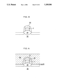
- the bit line contact hole 55d is formed between LOCOS films 70, 70 on a Si substrate 74 having the LOCOS films 70, SiO 2 films 71, capacitor insulating films 72 and a plate electrodes 73.
- the contact hole 53 for the node electrode is formed between the transfer gate 52 which is provided on the LOCOS film 70 and the transfer gate 52 which is provided through a gate oxide film 81 on the Si substrate 74 having impurity diffusion layers 80, 80.
- the contact hole 53 is buried by a capacitor 84 comprised of the node electrode 54, the capacitor insulating film 72 and the plate electrode 73.
- a short side m of the node electrode 54 is always set to the minimum dimension between the node electrodes 54, 54 which is defined by design rules. For this reason, the maximum projected area of the node electrode 54 is automatically determined by overlapping with each layer.
- the projected area of the node electrode is determined by overlapping with each layer. Consequently, when the cell size is specified, the cell capacity is determined.
- the cell size is reduced with the high integration of the LSI memory. Consequently, it becomes more difficult to ensure the cell capacity.
- the present invention provides a semiconductor memory wherein a plurality of cells are arranged in a longitudinal direction of active regions, each cell having a node electrode and a contact hole for the node electrode, and a bit line contact region and the active region by half at the least on a semiconductor substrate having the active regions and word lines which are extended in a direction perpendicular to the longitudinal direction of the active regions, the bit line contact regions of adjacent bit lines are shifted by a quarter in the longitudinal direction between the adjacent cells in a direction in which the word lines are extended, and the projected shape of the node electrode is a polygon having more angles than a quadrangle which is substantially adapted as the node electrode and having at least one of interior angles set to be obtuse so that the projected area is substantially larger than that of the quadrangle.
- the present invention further provides a semiconductor memory wherein the layout of the plate electrode does not exist between the adjacent bit line contact regions.
- FIG. 1 is a view showing the entire structure of one embodiment of the present invention
- FIG. 2 is a view showing the structure of a main portion of the embodiment
- FIG. 3 is a view shown in a direction of III--III in FIG. 2;
- FIG. 4 is a view shown in a direction of IV--IV in FIG. 2;
- FIG. 5 is a view showing the defects in a example
- FIG. 6 is a view showing the defects in the example
- FIG. 7 is a view showing the structure of a main portion in the example.
- FIG. 8 is a view showing the main portion of the defects in the example.
- FIGS. 9 to 12 are views showing a manufacturing method in the conventional example and seen in a direction of I--I in FIG. 7;
- FIGS. 13 to 16 are views showing the manufacturing method in the conventional example and seen in a direction of II--II in FIG. 7;
- FIG. 17 is a view showing a node electrode according to the embodiment.
- FIGS. 18 to 20 are views showing variants of the node electrode according to the present invention.
- FIG. 21 is a view showing the node electrode according to the conventional example.
- FIG. 22 is a view showing the entire structure of the conventional example.
- FIG. 23 is a view seen in a direction of V--V in FIG. 22.
- FIG. 24 is a view seen in a direction of VI--VI in FIG. 22.
- the present invention is characterized in that the projected shape of a node electrode is a polygon whose projected area is substantially larger than that of a quadrangle, bit line contact regions are arranged on a diagonal line, and the layout of a plate electrode does not exist between the adjacent bit line contact regions.
- bit line contacts of adjacent bit lines are shifted by a quarter of a cell length in a longitudinal direction of active regions so as to be mutually arranged in a direction in which word lines are extended.
- the node electrode of each cell has the projected shape of the polygon which has more angles than the quadrangle and in which at least one of interior angles is obtuse. Consequently, it is possible to ensure cell capacity which is larger than that of the folded bit line form for the same cell size.
- the node electrode of the present invention is the polygon whose projected area is substantially larger than that of the quadrangle.
- the projected shape of a conventional node electrode 54 shown in FIG. 22 is compared with that of a hexagonal node electrode 4 according to the present embodiment shown in FIG. 1.
- the projected shape of the conventional node electrode 54 is a rectangle of which long side l is extended in a direction of an arrow C.
- the hexagonal node electrode 4 has a long side l which is equal to that of the rectangle, a short side m which is equal to that of the rectangle and is perpendicular to the long side l, and four other sides.
- Interior angles ⁇ and ⁇ , which are formed by the four other sides, are set to obtuse ones. Consequently, a hexagon has the area which is larger than that of the rectangle shown in FIG. 22 by about 9%.
- the projected area of the hexagonal node electrode 4 of the present embodiment shown in FIG. 17 is compared with that of the conventional rectangular node electrode 54 shown in FIG. 21 as follows.
- the projected area N 1 of the node electrode 4 can be obtained by the following formula. ##EQU1##
- N 1 is greater than N 5 .
- the projected area can be increased by about 9%. Consequently, even if the cell size is reduced with high integration of an LSI memory, it is possible to ensure the larger cell capacity according to the present invention.
- the projected shape of the node electrode according to the present invention is not limited to a hexagon. It is desired that the projected area can be increased.
- a polygon having more angles than a quadrangle.
- bit line contact holes (5a) to (5e) are arranged on a diagonal line and which have a size S, of 6 ⁇ m in the C direction and a size S 3 of 2 ⁇ m in a direction of an arrow D as shown in FIG. 1.
- the plate electrode is removed so as not to exist among the bit line contact regions.
- FIG. 3 is a view seen in a direction of III--III in FIG. 2.
- FIG. 4 is a view seen in a direction of IV--IV in FIG. 2 (i.e., a view seen in a diagonal direction which is slightly shifted from FIG. 3).
- FIG. 7 shows a memory in which bit line contact holes (5a) to (5c) are arranged on a diagonal line.
- FIGS. 5 and 6 are views seen in a direction of II--II in FIG. 7.
- FIG. 8 is an enlarged view showing a main portion of FIG. 7.
- FIGS. 9 to 12 are views seen in a direction of I--I in FIG. 7.
- FIGS. 13 to 16 are views seen in a direction of II--II in FIG. 7.
- a LOCOS film (33) as an element separation film is formed on a P-type Si substrate (32).
- the LOCOS film (33) has a thickness d 1 of 4000 ⁇ .
- thermal oxidation is performed to form a gate oxide film (34) having a thickness d 5 of 150 ⁇ .
- a polysilicon layer having a thickness d 2 of 3000 ⁇ is laminated on the gate oxide film (34).
- Impurities phosphorus ions
- a SiO 2 film having a thickness d 3 of 2000 ⁇ is laminated on the impurities by a CVD method.
- a transfer gate (2) and a SiO 2 film (35) are formed by photoetching technique (see FIG. 13).
- Ions are injected over the entire surface of the Si substrate (32) including the transfer gate (2) so as to form a source (30) and a drain (31). Furthermore, a SiO 2 film is laminated at a thickness of 2500 ⁇ by the CVD method. The laminated SiO 2 film is etched back by reactive ion etching technique so as to form a side wall (36).
- a SiO 2 film (37) is laminated at a thickness of 1500 ⁇ by the CVD method as shown in FIG. 10. Thereafter, a resist film (38) (see FIG. 14) is used to form a contact hole (3) for the node electrode by the photoetching technique.
- a polysilicon layer is laminated at a thickness of 1500 ⁇ on the Si substrate including the contact hole (3) for the node electrode by the CVD method as shown in FIG. 11.
- the impurities phosphorus ions
- a resist film (40) is used to form a node electrode (4) by the photoetching technique.
- the SiO 2 film (37) (see FIG. 14) having a thickness of 1500 ⁇ , which is not covered by the resist film (40), is etched such that a SiO 2 film (39) having a thickness d 4 of 1000 ⁇ remains (see FIG. 15).
- a SiO 2 film having a thickness of 100 ⁇ and a polysilicon film having a thickness of 1500 ⁇ are sequentially laminated by the CVD method as shown in FIG. 12. Then, the impurities (phosphorus ions) are diffused over the polysilicon film. Thereafter, a resist pattern (41) for forming a plate electrode is used to form a plate electrode (6) and a capacitor insulating film (42) by the photoetching technique (see FIG. 16). Consequently, a memory having capacitor electrodes can be fabricated.
- the II--II portion has the level difference D 2 .
- FIG. 5 shows the case where unetched polysilicon (6a) is generated in the active regions (30) and (31), and the bit line contact (5a) comes into contact with the unetched polysilicon (6a) owing to alignment shift (see FIG. 8). Consequently, the plate electrode (6) and bit line contact (5a) may be short-circuited.
- FIG. 6 shows the worst case where the unetched polysilicon (6a) is generated owing to the alignment shift of the transfer gate (2) and plate electrode (6) so that the plate electrode (6) and bit line contact (5a) are short-circuited.
- the resist pattern has the configuration in which the plate electrode (6) is not formed in an oblique direction of the bit line contacts (5a) to (5c) (i.e., in a direction of III--III or IV--IV in FIG. 2) as shown in FIGS. 1 and 2.
- the plate electrode (6) is formed by the resist pattern (41).
- a pattern (not shown) having the layout in which the plate electrode does not remain on the SiO 2 film (39) as shown in FIGS. 3 and 4.
- FIG. 3 is a view seen in a direction of III--III in FIG. 2.
- FIG. 4 is a view seen in a direction of IV--IV which is slightly shifted from FIG. 3.
- the transfer gate (2) is apart from a LOCOS film end (33a) by a distance H. Consequently, a level difference D 4 can be obtained by the following formula. ##EQU5## In other words, D 4 is almost equal to D 3 in FIG. 12. Consequently, processing can easily be performed.
- the comparative example shown in FIG. 12 has the same structure as that of a view seen in a direction of V--V in FIG. 22.
- the stacked capacitor has a plurality of cells 16 to 20 arranged in a direction of an arrow C.
- Each cell has a contact 3 for a node electrode and a node electrode 4, and a bit line contact region 5a, 5b, 5c, 5d or 5e and active regions 30 and 31 by half at the least on a semiconductor substrate.
- the semiconductor substrate has the active regions 30 and 31, and word lines (transfer gates) 2.
- the word lines 2 are extended in a direction (a direction of an arrow D) perpendicular to a longitudinal direction of the active regions 30 and 31 (the C direction).
- bit line contact regions 5a to 5d of the cells 16 to 19 are mutually shifted by a quarter in the C direction among the adjacent cells in the D direction, for example, between the cells 16 and 17 and between the cells 18 and 19.
- the projected shape of the node electrode 4 is a hexagon.
- the hexagon has interior angles ⁇ and ⁇ which are obtuse, for example, in the cell 17.
- each cell has a size S 1 of 6 ⁇ m in the C direction and a size S 3 of 2 ⁇ m in the D direction.
- the present embodiment employs the above-mentioned structure. Consequently, the hexagonal node electrode of the present embodiment has the projected area which is larger than that of the conventional quadrangle by about 9% for the same cell size (2 ⁇ m ⁇ 6 ⁇ m). Accordingly, it is possible to ensure cell capacity which is larger by about 9%.
- the plate electrode layout 6 (see FIG. 2) has the configuration in which the bit line contacts (5a ) to (5c) are surrounded over the entire periphery thereof. According to the present embodiment, however, the plate electrode layout 6 does not exist among the bit line contacts (5a) to (5c).
- the unetched polysilicon projects into the active region owing to alignment shift on a high level difference portion in the region 5 among the bit line contacts (5a) to (5d). Consequently, the present embodiment (see FIG. 2) has the following structure in order to prevent the bit line contact 5a and unetched polysilicon from coming into contact with each other and being short-circuited.
- the plate electrode layout 6 does not exist among the bit line contacts (5a) to (5d), i.e., is penetrated in an oblique direction.
- the plate electrode layout is omitted in the oblique direction so that the plate electrode does not exist among the bit line contacts. Consequently, it is possible to eliminate the unetched polysilicon which is generated among the bit line contacts. Thus, the unetched polysilicon can be prevented from coming into contact with the bit line contact. As a result, there can be obtained a device having the higher yield and reliability.
- bit line contacts are respectively arranged by a quarter of the cell and the projected shape of the node electrode is the polygon which has more angles than the quadrangle. Consequently, it is possible to ensure the cell capacity which is larger than that of the folded bit line form for the same cell size.
Abstract
A semiconductor memory wherein a plurality of cells are arranged in a longitudinal direction of active regions, each cell having a node electrode and a contact hole for the node electrode, and a bit line contact region and the active region by half at the least on a semiconductor substrate having the active regions and word lines which are extended in a direction perpendicular to the longitudinal direction of the active regions, the bit line contact regions of adjacent bit lines are shifted by a quarter in the longitudinal direction between the adjacent cells in a direction in which the word lines are extended, and the projected shape of the node electrode is a polygon having more angles than a quadrangle which is substantially adapted as the node electrode and having at least one of interior angles set to be obtuse so that the projected area is substantially larger than that of the quadrangle.
Description
1. Field of the Invention
The present invention relates to a semiconductor memory, and more particularly to a MOS dynamic memory comprising a stacked memory capacitor.
2. Description of the Prior Art
To ensure cell capacity with high integration of an LSI memory, there has been developed and put to practical use a stacked memory capacitor in which the surface level difference among the lower layers of a semiconductor device is utilized on a three-dimensional basis.
FIG. 22 shows the layout of the stacked capacitor in the folded bit line form. In FIG. 22, the stacked capacitor has a plurality of cells 56 to 61 arranged in a direction of an arrows C and D. Each cell has a contact 53 for a node electrode and a node electrode 54, and a bit line contact region 55a, 55b, 55c, 55d or 55e and an active region 51 by half at the least on a semiconductor substrate. The semiconductor substrate has the active regions 51 and word lines (transfer gates) 52. The word lines 52 are extended in a direction (a direction of an arrow D) perpendicular to a longitudinal direction of the active regions 51 (the C direction).
The adjacent bit line contact regions 55a and 55b are arranged on the same line parallel with the D direction between the cells 56 and 57. In addition, the adjacent bit line contact regions 55c and 55d are arranged on the same line parallel with the D direction between the cells 58 and 59.
Furthermore, the projected shape of the node electrode 54 is a quadrangle which is adapted as a node electrode.
Each cell has a size S2 of 6 μm in the C direction, and a size S4 of 2 μm in the D direction.
As shown in FIGS. 23 and 24, the bit line contact region 55 includes a bit line contact hole 55d. The bit line contact hole 55d is formed between LOCOS films 70, 70 on a Si substrate 74 having the LOCOS films 70, SiO2 films 71, capacitor insulating films 72 and a plate electrodes 73. The contact hole 53 for the node electrode is formed between the transfer gate 52 which is provided on the LOCOS film 70 and the transfer gate 52 which is provided through a gate oxide film 81 on the Si substrate 74 having impurity diffusion layers 80, 80. The contact hole 53 is buried by a capacitor 84 comprised of the node electrode 54, the capacitor insulating film 72 and the plate electrode 73.
Referring to the memory in the folded bit line form, a short side m of the node electrode 54 is always set to the minimum dimension between the node electrodes 54, 54 which is defined by design rules. For this reason, the maximum projected area of the node electrode 54 is automatically determined by overlapping with each layer.
Referring to the cell layout mentioned above, however, the projected area of the node electrode is determined by overlapping with each layer. Consequently, when the cell size is specified, the cell capacity is determined.
Accordingly, the cell size is reduced with the high integration of the LSI memory. Consequently, it becomes more difficult to ensure the cell capacity.
The present invention provides a semiconductor memory wherein a plurality of cells are arranged in a longitudinal direction of active regions, each cell having a node electrode and a contact hole for the node electrode, and a bit line contact region and the active region by half at the least on a semiconductor substrate having the active regions and word lines which are extended in a direction perpendicular to the longitudinal direction of the active regions, the bit line contact regions of adjacent bit lines are shifted by a quarter in the longitudinal direction between the adjacent cells in a direction in which the word lines are extended, and the projected shape of the node electrode is a polygon having more angles than a quadrangle which is substantially adapted as the node electrode and having at least one of interior angles set to be obtuse so that the projected area is substantially larger than that of the quadrangle.
From another aspect, the present invention further provides a semiconductor memory wherein the layout of the plate electrode does not exist between the adjacent bit line contact regions.
FIG. 1 is a view showing the entire structure of one embodiment of the present invention;
FIG. 2 is a view showing the structure of a main portion of the embodiment;
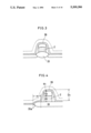
FIG. 3 is a view shown in a direction of III--III in FIG. 2;
FIG. 4 is a view shown in a direction of IV--IV in FIG. 2;
FIG. 5 is a view showing the defects in a example;
FIG. 6 is a view showing the defects in the example;
FIG. 7 is a view showing the structure of a main portion in the example;
FIG. 8 is a view showing the main portion of the defects in the example;
FIGS. 9 to 12 are views showing a manufacturing method in the conventional example and seen in a direction of I--I in FIG. 7;
FIGS. 13 to 16 are views showing the manufacturing method in the conventional example and seen in a direction of II--II in FIG. 7;
FIG. 17 is a view showing a node electrode according to the embodiment;
FIGS. 18 to 20 are views showing variants of the node electrode according to the present invention;
FIG. 21 is a view showing the node electrode according to the conventional example;
FIG. 22 is a view showing the entire structure of the conventional example;
FIG. 23 is a view seen in a direction of V--V in FIG. 22; and
FIG. 24 is a view seen in a direction of VI--VI in FIG. 22.
The present invention is characterized in that the projected shape of a node electrode is a polygon whose projected area is substantially larger than that of a quadrangle, bit line contact regions are arranged on a diagonal line, and the layout of a plate electrode does not exist between the adjacent bit line contact regions.
According to the present invention, bit line contacts of adjacent bit lines are shifted by a quarter of a cell length in a longitudinal direction of active regions so as to be mutually arranged in a direction in which word lines are extended. In addition, the node electrode of each cell has the projected shape of the polygon which has more angles than the quadrangle and in which at least one of interior angles is obtuse. Consequently, it is possible to ensure cell capacity which is larger than that of the folded bit line form for the same cell size.
The node electrode of the present invention is the polygon whose projected area is substantially larger than that of the quadrangle. The projected shape of a conventional node electrode 54 shown in FIG. 22 is compared with that of a hexagonal node electrode 4 according to the present embodiment shown in FIG. 1. The projected shape of the conventional node electrode 54 is a rectangle of which long side l is extended in a direction of an arrow C. The hexagonal node electrode 4 has a long side l which is equal to that of the rectangle, a short side m which is equal to that of the rectangle and is perpendicular to the long side l, and four other sides. Interior angles α and β, which are formed by the four other sides, are set to obtuse ones. Consequently, a hexagon has the area which is larger than that of the rectangle shown in FIG. 22 by about 9%.
More specifically, the projected area of the hexagonal node electrode 4 of the present embodiment shown in FIG. 17 is compared with that of the conventional rectangular node electrode 54 shown in FIG. 21 as follows.
In FIG. 17, l=2.5 μm, m=1.5 μm, n=t=0.5 μm, p=0.75 μm, q=r=1.25 μm, u=0.75 μm, and α=β=135°.
Accordingly, the projected area N1 of the node electrode 4 can be obtained by the following formula. ##EQU1##
In FIG. 21, l=2.5 μm and m=1.5 μm. Accordingly, the projected area N5 of the conventional node electrode can be obtained as follows. ##EQU2##
As described above, N1 is greater than N5. In addition, the projected area can be increased by about 9%. Consequently, even if the cell size is reduced with high integration of an LSI memory, it is possible to ensure the larger cell capacity according to the present invention.
Furthermore, the projected shape of the node electrode according to the present invention is not limited to a hexagon. It is desired that the projected area can be increased. By way of example, there can be used a pentagon (141) having the projected area of N2 (see FIG. 18), an octagon (142) having the projected area of N4 (see FIG. 20), a hexagon (143) of which shape is different from that of the above-mentioned hexagon and which has the projected area of N3, and a heptagon. In other words, there can be used a polygon having more angles than a quadrangle.
According to the present invention, there are provided cells in which bit line contact holes (5a) to (5e) are arranged on a diagonal line and which have a size S, of 6 μm in the C direction and a size S3 of 2 μm in a direction of an arrow D as shown in FIG. 1. In the cells, the plate electrode is removed so as not to exist among the bit line contact regions.
The foregoing will be described in more detail with reference to FIGS. 1 and 2, in particular to FIGS. 3 and 4. FIG. 3 is a view seen in a direction of III--III in FIG. 2. FIG. 4 is a view seen in a direction of IV--IV in FIG. 2 (i.e., a view seen in a diagonal direction which is slightly shifted from FIG. 3).
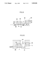
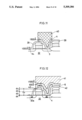
In this case, the advantages of the present embodiment will be described with reference to FIGS. 5 to 8 as comparative examples. FIG. 7 shows a memory in which bit line contact holes (5a) to (5c) are arranged on a diagonal line.
FIGS. 5 and 6 are views seen in a direction of II--II in FIG. 7. FIG. 8 is an enlarged view showing a main portion of FIG. 7.
There will generally be described a memory, in which the bit line contact regions are arranged on the diagonal line, with reference to FIG. 7 as the comparative example.
The memory will be described with reference to FIGS. 9 to 16. FIGS. 9 to 12 are views seen in a direction of I--I in FIG. 7. FIGS. 13 to 16 are views seen in a direction of II--II in FIG. 7.
As shown in FIG. 9, a LOCOS film (33) as an element separation film is formed on a P-type Si substrate (32). The LOCOS film (33) has a thickness d1 of 4000 Å. Then, thermal oxidation is performed to form a gate oxide film (34) having a thickness d5 of 150 Å. A polysilicon layer having a thickness d2 of 3000 Å is laminated on the gate oxide film (34). Impurities (phosphorus ions) are diffused over the polysilicon layer. Thereafter, a SiO2 film having a thickness d3 of 2000 Å is laminated on the impurities by a CVD method. A transfer gate (2) and a SiO2 film (35) are formed by photoetching technique (see FIG. 13). Ions are injected over the entire surface of the Si substrate (32) including the transfer gate (2) so as to form a source (30) and a drain (31). Furthermore, a SiO2 film is laminated at a thickness of 2500 Å by the CVD method. The laminated SiO2 film is etched back by reactive ion etching technique so as to form a side wall (36).
Then, a SiO2 film (37) is laminated at a thickness of 1500 Å by the CVD method as shown in FIG. 10. Thereafter, a resist film (38) (see FIG. 14) is used to form a contact hole (3) for the node electrode by the photoetching technique.
Subsequently, a polysilicon layer is laminated at a thickness of 1500 Å on the Si substrate including the contact hole (3) for the node electrode by the CVD method as shown in FIG. 11. The impurities (phosphorus ions) are diffused over the polysilicon layer. Then, a resist film (40) is used to form a node electrode (4) by the photoetching technique.
In this case, the SiO2 film (37) (see FIG. 14) having a thickness of 1500 Å, which is not covered by the resist film (40), is etched such that a SiO2 film (39) having a thickness d4 of 1000 Å remains (see FIG. 15).
Lastly, a SiO2 film having a thickness of 100 Å and a polysilicon film having a thickness of 1500 Å are sequentially laminated by the CVD method as shown in FIG. 12. Then, the impurities (phosphorus ions) are diffused over the polysilicon film. Thereafter, a resist pattern (41) for forming a plate electrode is used to form a plate electrode (6) and a capacitor insulating film (42) by the photoetching technique (see FIG. 16). Consequently, a memory having capacitor electrodes can be fabricated.
Referring to FIG. 12, there can be obtained a level difference D3 from a surface (32a) of active regions (30) and (31) on the Si substrate (32) to a lower face (43) of the capacitor electrode by the following formula. ##EQU3##
Referring to FIG. 16, there can be obtained a level difference D2 from the surface (32a) of the active regions to a lower face (44) of the capacitor electrode by the following formula. ##EQU4##
Referring to FIG. 7 as the comparative example, the II--II portion has the level difference D2. The level difference D2 is larger than the level difference D3 of the I--I portion by ΔD (about 1850 Å) which is about half the thickness d1 of the LOCOS film (33). Accordingly, in the case where the plate electrode (6) is to be formed by the resist pattern (41) in FIGS. 12 and 16, it is necessary to perform excessive etching by the increase of the level difference, i.e., ΔD (=D2 -D3).
With the memory having the structure shown in FIG. 7, it is difficult to obtain the shape shown in FIG. 16. When the polysilicon layer having a thickness of 1500 Å is etched by the resist pattern (41), unetched polysilicon remains in the active regions (30) and (31) as shown in FIGS. 5, 6 and 8.
FIG. 5 shows the case where unetched polysilicon (6a) is generated in the active regions (30) and (31), and the bit line contact (5a) comes into contact with the unetched polysilicon (6a) owing to alignment shift (see FIG. 8). Consequently, the plate electrode (6) and bit line contact (5a) may be short-circuited.
FIG. 6 shows the worst case where the unetched polysilicon (6a) is generated owing to the alignment shift of the transfer gate (2) and plate electrode (6) so that the plate electrode (6) and bit line contact (5a) are short-circuited.
To avoid the above-mentioned drawbacks, the resist pattern has the configuration in which the plate electrode (6) is not formed in an oblique direction of the bit line contacts (5a) to (5c) (i.e., in a direction of III--III or IV--IV in FIG. 2) as shown in FIGS. 1 and 2.
Referring to FIG. 16, in the case where the periphery of the bit line contact regions (5a) to (5d) is to be removed, the plate electrode (6) is formed by the resist pattern (41). According to the present invention, there is used a pattern (not shown) having the layout in which the plate electrode does not remain on the SiO2 film (39) as shown in FIGS. 3 and 4. FIG. 3 is a view seen in a direction of III--III in FIG. 2. FIG. 4 is a view seen in a direction of IV--IV which is slightly shifted from FIG. 3.
Referring to FIG. 4, the transfer gate (2) is apart from a LOCOS film end (33a) by a distance H. Consequently, a level difference D4 can be obtained by the following formula. ##EQU5## In other words, D4 is almost equal to D3 in FIG. 12. Consequently, processing can easily be performed. The comparative example shown in FIG. 12 has the same structure as that of a view seen in a direction of V--V in FIG. 22.
An embodiment of the present invention will be described in more detail with reference to the drawings. The present invention is not limited to the embodiment to be described below.
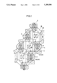
In FIG. 1, the stacked capacitor has a plurality of cells 16 to 20 arranged in a direction of an arrow C. Each cell has a contact 3 for a node electrode and a node electrode 4, and a bit line contact region 5a, 5b, 5c, 5d or 5e and active regions 30 and 31 by half at the least on a semiconductor substrate. The semiconductor substrate has the active regions 30 and 31, and word lines (transfer gates) 2. The word lines 2 are extended in a direction (a direction of an arrow D) perpendicular to a longitudinal direction of the active regions 30 and 31 (the C direction).
Furthermore, the bit line contact regions 5a to 5d of the cells 16 to 19 are mutually shifted by a quarter in the C direction among the adjacent cells in the D direction, for example, between the cells 16 and 17 and between the cells 18 and 19.
In addition, the projected shape of the node electrode 4 is a hexagon. The hexagon has interior angles α and β which are obtuse, for example, in the cell 17.
Furthermore, each cell has a size S1 of 6 μm in the C direction and a size S3 of 2 μm in the D direction.
The present embodiment employs the above-mentioned structure. Consequently, the hexagonal node electrode of the present embodiment has the projected area which is larger than that of the conventional quadrangle by about 9% for the same cell size (2 μm×6 μm). Accordingly, it is possible to ensure cell capacity which is larger by about 9%.
In the conventional example shown in FIG. 7, the plate electrode layout 6 (see FIG. 2) has the configuration in which the bit line contacts (5a ) to (5c) are surrounded over the entire periphery thereof. According to the present embodiment, however, the plate electrode layout 6 does not exist among the bit line contacts (5a) to (5c).
As shown in FIGS. 7 and 8, the unetched polysilicon projects into the active region owing to alignment shift on a high level difference portion in the region 5 among the bit line contacts (5a) to (5d). Consequently, the present embodiment (see FIG. 2) has the following structure in order to prevent the bit line contact 5a and unetched polysilicon from coming into contact with each other and being short-circuited. In other words, the plate electrode layout 6 does not exist among the bit line contacts (5a) to (5d), i.e., is penetrated in an oblique direction.
For this reason, even if the alignment shift occurs caused, the bit line contact and unetched polysilicon can be prevented from coming into contact with each other and being short-circuited. Consequently, yield can be enhanced and high reliability can be obtained. Thus, it is possible to realize the layout of a memory cell which has good productivity.
According to the present invention, the plate electrode layout is omitted in the oblique direction so that the plate electrode does not exist among the bit line contacts. Consequently, it is possible to eliminate the unetched polysilicon which is generated among the bit line contacts. Thus, the unetched polysilicon can be prevented from coming into contact with the bit line contact. As a result, there can be obtained a device having the higher yield and reliability.
Furthermore, the bit line contacts are respectively arranged by a quarter of the cell and the projected shape of the node electrode is the polygon which has more angles than the quadrangle. Consequently, it is possible to ensure the cell capacity which is larger than that of the folded bit line form for the same cell size.
Claims (9)
1. A semiconductor memory comprising:
a plurality of cells formed on a semiconductor substrate, the cells having active regions extending substantially in a longitudinal direction, each cell having a node electrode, a contact hole for the node electrode, and a bit line contact region,
word lines extending in a direction perpendicular to the longitudinal direction of the active regions,
bit lines extending in a longitudinal direction,
wherein the bit line contact regions of two adjacent cells which are connected to different yet adjacent bit lines are shifted with respect to the longitudinal direction by a distance which is one quarter of a length between two adjacent bit contact regions which are connected to a common bit line; and
the node electrode is shaped as a polygon having at least five interior angles, at least one of the interior angles being an obtuse angle.
2. The semiconductor memory of claim 1, wherein the polygon has an area which is greater than 3.75 μm2.
3. The semiconductor memory of claim 1, wherein the polygon is a pentagon.
4. The semiconductor memory of claim 1, wherein the polygon is a hexagon.
5. The semiconductor memory of claim 1, wherein the polygon is a heptagon
6. The semiconductor memory of claim 1, wherein the polygon is a octagon.
7. The semiconductor memory of claim 1, further comprising a plate electrode formed in a position other than between adjacent bit line contact regions.
8. The semiconductor memory of claim 7, further comprising a plate electrode formed in a position other than in a diagonal direction between adjacent bit line contact regions.
9. A semiconductor memory according to claim 7, wherein the plate electrode is formed by magnetron etcher for 195 seconds at a RF power of 300 W, a pressure of 100 mTorr and a magnetic flux density of 75 Gauss in the mixed gas atmosphere of chlorine gas (Cl2) of 54 SCCM, hydrogen bromide (HBr) of 66 SCCM and oxygen gas (O2) of 2 SCCM.
Applications Claiming Priority (4)
| Application Number | Priority Date | Filing Date | Title |
|---|---|---|---|
| JP2123583A JP2515037B2 (en) | 1990-05-14 | 1990-05-14 | Semiconductor memory |
| JP2-123583 | 1990-05-14 | ||
| JP2-129706 | 1990-05-18 | ||
| JP2129706A JP2512598B2 (en) | 1990-05-18 | 1990-05-18 | Semiconductor memory |
Publications (1)
| Publication Number | Publication Date |
|---|---|
| US5309386A true US5309386A (en) | 1994-05-03 |
Family
ID=26460468
Family Applications (1)
| Application Number | Title | Priority Date | Filing Date |
|---|---|---|---|
| US07/699,348 Expired - Lifetime US5309386A (en) | 1990-05-14 | 1991-05-13 | Semiconductor memory with enhanced capacity |
Country Status (1)
| Country | Link |
|---|---|
| US (1) | US5309386A (en) |
Cited By (7)
| Publication number | Priority date | Publication date | Assignee | Title |
|---|---|---|---|---|
| US5548548A (en) * | 1994-03-21 | 1996-08-20 | Texas Instruments Incorporated | Pass transistor for a 256 megabit dram with negatively biased substrate |
| US5578849A (en) * | 1993-11-19 | 1996-11-26 | Hitachi, Ltd. | Semiconductor integrated circuit device including a memory device having memory cells with increased information storage capacitance |
| US5734184A (en) * | 1995-12-21 | 1998-03-31 | Texas Instruments Incorporated | DRAM COB bit line and moat arrangement |
| US5822241A (en) * | 1996-07-29 | 1998-10-13 | Texas Instruments Incorporated | DRAM pass transistors |
| US6580175B1 (en) * | 1999-11-15 | 2003-06-17 | Samsung Electronics Co., Ltd. | Semiconductor layout structure for a conductive layer and contact hole |
| US7462903B1 (en) * | 2005-09-14 | 2008-12-09 | Spansion Llc | Methods for fabricating semiconductor devices and contacts to semiconductor devices |
| US20090283921A1 (en) * | 2008-05-19 | 2009-11-19 | Wen-Chieh Wang | Contact layout structure |
Citations (4)
| Publication number | Priority date | Publication date | Assignee | Title |
|---|---|---|---|---|
| US4300212A (en) * | 1979-01-24 | 1981-11-10 | Xicor, Inc. | Nonvolatile static random access memory devices |
| US4464734A (en) * | 1980-04-07 | 1984-08-07 | Texas Instruments Incorporated | Semiconductor dynamic memory cell array with word lines extending into windows of capacitor plate |
| US4763299A (en) * | 1985-10-15 | 1988-08-09 | Emanuel Hazani | E2 PROM cell and architecture |
| US5140389A (en) * | 1988-01-08 | 1992-08-18 | Hitachi, Ltd. | Semiconductor memory device having stacked capacitor cells |
-
1991
- 1991-05-13 US US07/699,348 patent/US5309386A/en not_active Expired - Lifetime
Patent Citations (4)
| Publication number | Priority date | Publication date | Assignee | Title |
|---|---|---|---|---|
| US4300212A (en) * | 1979-01-24 | 1981-11-10 | Xicor, Inc. | Nonvolatile static random access memory devices |
| US4464734A (en) * | 1980-04-07 | 1984-08-07 | Texas Instruments Incorporated | Semiconductor dynamic memory cell array with word lines extending into windows of capacitor plate |
| US4763299A (en) * | 1985-10-15 | 1988-08-09 | Emanuel Hazani | E2 PROM cell and architecture |
| US5140389A (en) * | 1988-01-08 | 1992-08-18 | Hitachi, Ltd. | Semiconductor memory device having stacked capacitor cells |
Cited By (13)
| Publication number | Priority date | Publication date | Assignee | Title |
|---|---|---|---|---|
| CN1303693C (en) * | 1993-11-19 | 2007-03-07 | 株式会社日立制作所 | Semiconductor memory device |
| US5578849A (en) * | 1993-11-19 | 1996-11-26 | Hitachi, Ltd. | Semiconductor integrated circuit device including a memory device having memory cells with increased information storage capacitance |
| US5831300A (en) * | 1993-11-19 | 1998-11-03 | Hitachi, Ltd. | Semiconductor integrated circuit device including a memory device having memory cells with increased information storage capacitance and method of manufacturing same |
| US6023084A (en) * | 1993-11-19 | 2000-02-08 | Hitachi, Ltd. | Semiconductor integrated circuit device including a memory device having memory cells with increased information storage capacitance and method of manufacturing same |
| US5548548A (en) * | 1994-03-21 | 1996-08-20 | Texas Instruments Incorporated | Pass transistor for a 256 megabit dram with negatively biased substrate |
| US5734184A (en) * | 1995-12-21 | 1998-03-31 | Texas Instruments Incorporated | DRAM COB bit line and moat arrangement |
| US5822241A (en) * | 1996-07-29 | 1998-10-13 | Texas Instruments Incorporated | DRAM pass transistors |
| US6580175B1 (en) * | 1999-11-15 | 2003-06-17 | Samsung Electronics Co., Ltd. | Semiconductor layout structure for a conductive layer and contact hole |
| US7462903B1 (en) * | 2005-09-14 | 2008-12-09 | Spansion Llc | Methods for fabricating semiconductor devices and contacts to semiconductor devices |
| US20090283921A1 (en) * | 2008-05-19 | 2009-11-19 | Wen-Chieh Wang | Contact layout structure |
| US7830025B2 (en) | 2008-05-19 | 2010-11-09 | United Microelectronics Corp. | Contact layout structure |
| US20110024921A1 (en) * | 2008-05-19 | 2011-02-03 | Wen-Chieh Wang | Contact layout structure |
| US8026617B2 (en) | 2008-05-19 | 2011-09-27 | United Microelectronics Corp. | Contact layout structure |
Similar Documents
| Publication | Publication Date | Title |
|---|---|---|
| JP3368002B2 (en) | Semiconductor storage device | |
| US5196365A (en) | Method of making semiconductor memory device having stacked capacitor | |
| US5373170A (en) | Semiconductor memory device having a compact symmetrical layout | |
| US5828096A (en) | Semiconductor device having a contact hole | |
| KR900008649B1 (en) | Semiconductor memory device and method for manufacturing thereof | |
| US5290726A (en) | DRAM cells having stacked capacitors of fin structures and method of making thereof | |
| JPH07263576A (en) | Semiconductor integrated circuit device and manufacture thereof | |
| US6072241A (en) | Semiconductor device with self-aligned contact and its manufacture | |
| KR940006681B1 (en) | Stacked trench cell and fabricating method thereof | |
| US5309386A (en) | Semiconductor memory with enhanced capacity | |
| JPH0648719B2 (en) | Semiconductor memory device | |
| JPH11330418A (en) | Semiconductor device and its manufacture | |
| KR0137229B1 (en) | Semiconductor memory device and fabrication method thereof | |
| JPH06104397A (en) | Dynamic random-access memory cell and its manufacture | |
| US5574680A (en) | Semiconductor memory device | |
| US5913129A (en) | Method of fabricating a capacitor structure for a dynamic random access memory | |
| US6818505B2 (en) | Non-volatile semiconductor memory device and manufacturing method thereof | |
| KR0161438B1 (en) | Semiconductor memory device and manufacture thereof | |
| US6355517B1 (en) | Method for fabricating semiconductor memory with a groove | |
| US5270239A (en) | Method for manufacturing a dynamic random access memory cell | |
| JPH0294564A (en) | Manufacture of semiconductor device | |
| KR100576083B1 (en) | Semiconductor device and method of manufacturing semiconductor device | |
| US5242852A (en) | Method for manufacturing a semiconductor memory device | |
| JPS6058662A (en) | Memory device for temporary storage of charge | |
| KR19990077780A (en) | Semiconductor device and manufacturing method of the same |
Legal Events
| Date | Code | Title | Description |
|---|---|---|---|
| AS | Assignment |
Owner name: SHARP KABUSHIKI KAISHA, JAPAN Free format text: ASSIGNMENT OF ASSIGNORS INTEREST.;ASSIGNORS:YUSUKI, TATSUSHI;MIURA, ATSUSHI;TANAKA, KENICHI;REEL/FRAME:005706/0726 Effective date: 19910322 |
|
| STCF | Information on status: patent grant |
Free format text: PATENTED CASE |
|
| FEPP | Fee payment procedure |
Free format text: PAYOR NUMBER ASSIGNED (ORIGINAL EVENT CODE: ASPN); ENTITY STATUS OF PATENT OWNER: LARGE ENTITY |
|
| FPAY | Fee payment |
Year of fee payment: 4 |
|
| FPAY | Fee payment |
Year of fee payment: 8 |
|
| FPAY | Fee payment |
Year of fee payment: 12 |