US5313094A - Thermal dissipation of integrated circuits using diamond paths - Google Patents
Thermal dissipation of integrated circuits using diamond paths Download PDFInfo
- Publication number
- US5313094A US5313094A US07/827,195 US82719592A US5313094A US 5313094 A US5313094 A US 5313094A US 82719592 A US82719592 A US 82719592A US 5313094 A US5313094 A US 5313094A
- Authority
- US
- United States
- Prior art keywords
- substrate
- trench
- diamond
- silicon
- diamond filled
- Prior art date
- Legal status (The legal status is an assumption and is not a legal conclusion. Google has not performed a legal analysis and makes no representation as to the accuracy of the status listed.)
- Expired - Fee Related
Links
Images


Classifications
-
- H—ELECTRICITY
- H01—ELECTRIC ELEMENTS
- H01L—SEMICONDUCTOR DEVICES NOT COVERED BY CLASS H10
- H01L23/00—Details of semiconductor or other solid state devices
- H01L23/28—Encapsulations, e.g. encapsulating layers, coatings, e.g. for protection
- H01L23/31—Encapsulations, e.g. encapsulating layers, coatings, e.g. for protection characterised by the arrangement or shape
- H01L23/3157—Partial encapsulation or coating
- H01L23/3178—Coating or filling in grooves made in the semiconductor body
-
- H—ELECTRICITY
- H01—ELECTRIC ELEMENTS
- H01L—SEMICONDUCTOR DEVICES NOT COVERED BY CLASS H10
- H01L23/00—Details of semiconductor or other solid state devices
- H01L23/34—Arrangements for cooling, heating, ventilating or temperature compensation ; Temperature sensing arrangements
- H01L23/36—Selection of materials, or shaping, to facilitate cooling or heating, e.g. heatsinks
- H01L23/373—Cooling facilitated by selection of materials for the device or materials for thermal expansion adaptation, e.g. carbon
- H01L23/3732—Diamonds
-
- H—ELECTRICITY
- H01—ELECTRIC ELEMENTS
- H01L—SEMICONDUCTOR DEVICES NOT COVERED BY CLASS H10
- H01L2924/00—Indexing scheme for arrangements or methods for connecting or disconnecting semiconductor or solid-state bodies as covered by H01L24/00
- H01L2924/0001—Technical content checked by a classifier
- H01L2924/0002—Not covered by any one of groups H01L24/00, H01L24/00 and H01L2224/00
Definitions
- This invention relates to thermal dissipation techniques for integrated circuits and more particularly to an improved thermal dissipation technique for high density integrated circuits utilizing diamond trenches or holes.
- An object of the present invention is to provide a technique to dissipate thermal energy from isolated silicon regions.
- Another object of the present invention is to provide a technique to help to dissipate thermal energy from isolated silicon regions that can be utilized in VLSI technology.
- dissipation of thermal energy from isolated active silicon regions is provided by etching a trench or hole through the isolated active silicon regions and the underlying dielectric layer to the supportive silicon substrate; oxidizing the walls of the trench or hole; and, filling the trench or hole with CVD diamond material.
- the present invention provides for electrical isolation of active regions of silicon while providing excellent thermal dissipation characteristics.
- the present invention can be utilized for VLSI technology because the thermal dissipation structures use the existing electrical isolation trenches utilized in the prior art.
- the present invention is easy to incorporate and minimizes less thermal expansion problems which plague prior art electrical isolation techniques.
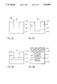
- FIG. 1A-1F are cross sectional views of the structure resultant from the steps for producing a conductive thermal path in accordance with a first embodiment of the present invention.
- FIGS. 2A-2F are cross sectional views of the structure resultant from the steps for producing a conductive thermal path in accordance with a second embodiment of the present invention.
- FIGS. 3A-3D are cross sectional views of the structure resultant from the steps for producing a conductive thermal path in accordance with a third embodiment of the present invention.
- FIGS. 4A-4D are cross sectional views of the structure resultant from the steps for producing a conductive thermal path in accordance with a fourth embodiment of the present invention.
- an isolated silicon structure 10 is comprised of an underlying silicon substrate 12, an intermediate isolation layer 14 comprised of an electrically insulative material, such as silicon dioxide or nitride, a top active isolated region 16 of silicon to which devices are to be built upon and a dielectric layer 17, such as nitride/oxide.
- a trench or hole 18 is patterned through the dielectric layer 17, silicon region 16, and isolation layer 14, and further into the silicon substrate 12 utilizing patterning techniques well known in the art, such as RIE.
- a thin thermal oxide layer 20 is formed on the walls and bottom of the trench 18 utilizing thermal oxidation techniques well known in the art. It is preferable that the thickness of the oxide layer be on the order of 300 angstroms. The purpose of having this layer 20 is to keep CVD diamond (described hereinafter) from directly contacting the silicon surface to avoid excessive surface charges. Thin oxide layer 20 is a passivation layer.
- a CVD diamond or diamond like layer 22 is deposited over the structure utilizing techniques well known in the art, thereby forming a diamond filled trench or hole 23.
- An example of CVD diamond deposition is found in U.S. Pat. No. 3,840,451 (Golyanov, et al.) which is hereby incorporated herein by reference.
- Diamond can be deposited over a wide range of deposition temperatures (200° C. to 1,000° C.) using a variety of hydrocarbon precursors (i.e. CH 4 , C 2 H 6 ) using either a RF or microwave generated plasma.
- Deposition conditions for downstream microwave generated diamond films are: a frequency of 2.45 GHz, power of 200-2,000 watts, a pressure of 0.1-100 Torr, a gas flow of 10-500 sccm, and a substrate temperature of 200°-1,000° C.
- the substrate is also biased with greater than a -100 Vdc or an RF bias of greater than -5 V.
- Diamond films deposited are polycrystalline or amorphous in nature with average grain size between 50 - 300 angstroms. The diamond layer 22 should completely fill the trench 18.
- the diamond film 22 is well suited for the present application because it has a low dielectric constant (3-6 depending on process conditions), high electrical resistivity (1E10 to 1E16 ohms/cm) and a matched thermal expansion coefficient with silicon (e.g. silicon: 32E-7/C, diamond: 18E-7/C, oxide: 6E-7/C).
- the film deposited 22 has a low compressive stress and after being annealed at 500° C., the stress is reduced to a non-measurable level.
- the resultant diamond filled trench or hole 23 provides a heat conductive path to dissipate thermal energy from the active silicon region 16 to the substrate 12.
- the diamond layer 22 is planarized using techniques well known in the art, such as O 2 /Ar RIE. This etching technique removes the diamond layer 22 from the top of the dielectric layer 17 and recesses the diamond filled trench or hole 23 below the top of the dielectric layer 17 to thereby create a recess area 24.
- the recess area 24 is then filled with intrinsic polysilicon, utilizing deposition techniques well known in the art, such as CVD.
- the polysilicon layer 26 is then polished back to the top of the dielectric layer 17.
- the polysilicon cap 26 is then oxidized to form an oxide cap 28 on top of the diamond filled trench 18.
- other insulators such as nitrides, may be utilized to cap the trench 18. It is to be noted that the insulative cap 28 is necessary to protect the diamond inside the trench 18 from being unintentionally removed during subsequent oxygen plasma processing, such as resist ashing or the like.
- a second embodiment in accordance with the present invention includes a structure 100 comprised of a silicon substrate 112 having an insulative layer 114 which separates the silicon substrate 112 from an active silicon region 116 to which devices are to be built thereon.
- a dielectric layer 117 is needed to passivate the silicon surface.
- a trench or hole 118 is patterned through the dielectric layer 117, silicon layer 116 and the insulation layer 114, and further into the substrate 112. Layers 112-117 and trench 118 are similar to the structure described and illustrated hereinbefore in FIG. 1A.
- a vertical implant is performed on the bottom of the trench 118 with a N dopant, such as Arsenic, and driven into the substrate 112.
- the subsequent doped region is illustrated by area 119.
- different dopant techniques may be utilized, it is important that the characteristic etch response of the resultant doped area 119 be different from that of the substrate 112.
- the doped area 119 is etched away using selective lateral etching techniques well known in the art, such as wet etch or selective plasma etch to thereby form a void or cavity 121 below trench 118.
- a thin insulative layer 120 of an insulator such as a thermal oxide is formed onto the walls and bottom of trench 118 and void or cavity 121.
- the preferred thickness of the layer 120 is on the order of 300 angstroms.
- a layer of CVD diamond or Diamond-like material 122 is then deposited over the structure 100 in a manner similar to that described and illustrated hereinbefore in FIG. 1C, to thereby form a diamond filled trench or hole 123.
- the increased amount of diamond which consequently fills cavity 121 provides greater surface area than that illustrated in FIG. 1C and therefore provides improved heat dissipation for devices built on layer 116.
- the diamond layer 122 is then planarized to create a recess 124 which is filled with a polysilicon layer 126, planarized and oxidized to thereby form an oxide cap 128 in a manner similar to that described and illustrated hereinbefore in FIGS. 1D-1F.
- a third embodiment of the present invention includes a structure 200 comprising a silicon substrate 212, an insulation layer 214, a silicon layer 216 and a dielectric layer 217.
- a trench or hole 218 is patterned through only the dielectric layer 217 and silicon layer 216 by using a CF 4 and Cl 2 plasma subsequently.
- a thin layer 220 of oxide is formed on the walls of trench 218.
- a directional oxide RIE is then used to continue patterning the trench 218 through layer 214 and into substrate 212.
- a CVD diamond layer 224 is deposited over the structure 200, thereby forming a diamond filled trench or hole 223.
- the remaining steps for the third embodiment thereafter continues identically to the steps of the first embodiment as described and illustrated in FIGS. 1D-1F.
- FIG. 3C The difference between FIG. 3C and FIG. 1B is that the bottom of the trench is not covered by the oxide layer. This approach will further improve the thermal dissipation to remove heat from the devices on 216 to substrate 212.
- a fourth embodiment in accordance with the present invention includes a structure 300 similar to structure 200 described and illustrated hereinbefore in FIG. 3C, having a silicon substrate 312, an insulation layer 314, a silicon layer 316 and a dielectric layer 317.
- a trench or hole 318 is patterned through layers 317, 316, 314 into substrate 312. Subsequent to the patterning of trench 318 through layers 317 and 316 and prior to the patterning of trench 318 through layer 314 and into substrate 312, a thin oxide layer 320 is formed on the walls of trench 318.
- a N+implant region 319 having a characteristic etch response different from that of the substrate 312 is provided at the bottom of the trench 318.
- a selective etching technique is utilized to remove N+implanted region 319 to thereby form a cavity 321.
- a CVD diamond layer 324 is deposited over structure 300, thereby forming a diamond filled trench or hole 323 and the remaining steps of the fourth embodiment proceed exactly as in accordance with the second embodiment described and illustrated hereinbefore in FIGS. 2C-2F. It is to be noted that the increased amount of diamond which consequently fills cavity 321 provides greater surface area than that illustrated in FIG. 3D and therefore provides improved heat dissipation for devices built on layer 316.
Abstract
A heat dissipation apparatus for dissipation of thermal energy from an isolated active silicon region to an underlying supportive substrate is disclosed. Such an apparatus comprises a diamond filled trench having walls extending through the isolated active silicon region, an underlying insulative layer, and into the supportive substrate, whereby said diamond filled trench provides a high thermal conductive path from said active silicon region to said substrate.
Description
This invention relates to thermal dissipation techniques for integrated circuits and more particularly to an improved thermal dissipation technique for high density integrated circuits utilizing diamond trenches or holes.
It is well known in the art to isolate regions of silicon from one another on a silicon substrate for the purpose of making active devices in the isolated regions. The most recent techniques for doing this involve isolating a layer of silicon vertically from an underlying silicon substrate with a dielectric layer, (commonly referred to as silicon on insulator or SOI). The advantages of having silicon devices on an insulator over bulk silicon substrates are that it provides higher packing density due to better isolation properties, simplified fabrication technology, radiation hardened capabilities, higher speeds due to fully depleted structures, and higher latch-up immunity. The above mentioned advantages to silicon on insulator structures are somewhat off set, however, by heat dissipation problems due to the fact that the isolating insulators have both a low electrical conductivity and low thermal conductivity. Poor power dissipation therefore imposes a considerable constraint for development of high speed/high power circuits on the isolated silicon regions.
A technique which resolves these thermal dissipation problems by providing a high thermal conductive path from the isolated silicon regions to the underlying silicon substrate is therefore highly desirable.
An object of the present invention is to provide a technique to dissipate thermal energy from isolated silicon regions.
Another object of the present invention is to provide a technique to help to dissipate thermal energy from isolated silicon regions that can be utilized in VLSI technology.
According to the present invention, dissipation of thermal energy from isolated active silicon regions is provided by etching a trench or hole through the isolated active silicon regions and the underlying dielectric layer to the supportive silicon substrate; oxidizing the walls of the trench or hole; and, filling the trench or hole with CVD diamond material.
The present invention provides for electrical isolation of active regions of silicon while providing excellent thermal dissipation characteristics. The present invention can be utilized for VLSI technology because the thermal dissipation structures use the existing electrical isolation trenches utilized in the prior art. In addition, the present invention is easy to incorporate and minimizes less thermal expansion problems which plague prior art electrical isolation techniques.
These and other objects, features and advantages of the present invention will be more apparent in light of the detailed description of exemplary embodiments thereof as illustrated by the drawings.
FIG. 1A-1F are cross sectional views of the structure resultant from the steps for producing a conductive thermal path in accordance with a first embodiment of the present invention.
FIGS. 2A-2F are cross sectional views of the structure resultant from the steps for producing a conductive thermal path in accordance with a second embodiment of the present invention.
FIGS. 3A-3D are cross sectional views of the structure resultant from the steps for producing a conductive thermal path in accordance with a third embodiment of the present invention.
FIGS. 4A-4D are cross sectional views of the structure resultant from the steps for producing a conductive thermal path in accordance with a fourth embodiment of the present invention.
Referring now to FIG. 1A, an isolated silicon structure 10 is comprised of an underlying silicon substrate 12, an intermediate isolation layer 14 comprised of an electrically insulative material, such as silicon dioxide or nitride, a top active isolated region 16 of silicon to which devices are to be built upon and a dielectric layer 17, such as nitride/oxide. A trench or hole 18 is patterned through the dielectric layer 17, silicon region 16, and isolation layer 14, and further into the silicon substrate 12 utilizing patterning techniques well known in the art, such as RIE.
Referring now to FIG. 1B, a thin thermal oxide layer 20 is formed on the walls and bottom of the trench 18 utilizing thermal oxidation techniques well known in the art. It is preferable that the thickness of the oxide layer be on the order of 300 angstroms. The purpose of having this layer 20 is to keep CVD diamond (described hereinafter) from directly contacting the silicon surface to avoid excessive surface charges. Thin oxide layer 20 is a passivation layer.
Referring now to FIG. 1C, a CVD diamond or diamond like layer 22 is deposited over the structure utilizing techniques well known in the art, thereby forming a diamond filled trench or hole 23. An example of CVD diamond deposition is found in U.S. Pat. No. 3,840,451 (Golyanov, et al.) which is hereby incorporated herein by reference. Diamond can be deposited over a wide range of deposition temperatures (200° C. to 1,000° C.) using a variety of hydrocarbon precursors (i.e. CH4, C2 H6) using either a RF or microwave generated plasma. Deposition conditions for downstream microwave generated diamond films are: a frequency of 2.45 GHz, power of 200-2,000 watts, a pressure of 0.1-100 Torr, a gas flow of 10-500 sccm, and a substrate temperature of 200°-1,000° C. The substrate is also biased with greater than a -100 Vdc or an RF bias of greater than -5 V. Diamond films deposited are polycrystalline or amorphous in nature with average grain size between 50 - 300 angstroms. The diamond layer 22 should completely fill the trench 18. The diamond film 22 is well suited for the present application because it has a low dielectric constant (3-6 depending on process conditions), high electrical resistivity (1E10 to 1E16 ohms/cm) and a matched thermal expansion coefficient with silicon (e.g. silicon: 32E-7/C, diamond: 18E-7/C, oxide: 6E-7/C). In addition, the film deposited 22 has a low compressive stress and after being annealed at 500° C., the stress is reduced to a non-measurable level. The resultant diamond filled trench or hole 23 provides a heat conductive path to dissipate thermal energy from the active silicon region 16 to the substrate 12.
Referring now to FIG. 1D, the diamond layer 22 is planarized using techniques well known in the art, such as O2 /Ar RIE. This etching technique removes the diamond layer 22 from the top of the dielectric layer 17 and recesses the diamond filled trench or hole 23 below the top of the dielectric layer 17 to thereby create a recess area 24.
Referring now to FIG. 1E, the recess area 24 is then filled with intrinsic polysilicon, utilizing deposition techniques well known in the art, such as CVD. The polysilicon layer 26 is then polished back to the top of the dielectric layer 17.
Referring now to FIG. 1F, the polysilicon cap 26 is then oxidized to form an oxide cap 28 on top of the diamond filled trench 18. Alternatively, other insulators, such as nitrides, may be utilized to cap the trench 18. It is to be noted that the insulative cap 28 is necessary to protect the diamond inside the trench 18 from being unintentionally removed during subsequent oxygen plasma processing, such as resist ashing or the like.
Referring now to FIG. 2A, a second embodiment in accordance with the present invention includes a structure 100 comprised of a silicon substrate 112 having an insulative layer 114 which separates the silicon substrate 112 from an active silicon region 116 to which devices are to be built thereon. A dielectric layer 117 is needed to passivate the silicon surface. A trench or hole 118 is patterned through the dielectric layer 117, silicon layer 116 and the insulation layer 114, and further into the substrate 112. Layers 112-117 and trench 118 are similar to the structure described and illustrated hereinbefore in FIG. 1A. After the trench or hole 118 is provided, a vertical implant is performed on the bottom of the trench 118 with a N dopant, such as Arsenic, and driven into the substrate 112. The subsequent doped region is illustrated by area 119. Although different dopant techniques may be utilized, it is important that the characteristic etch response of the resultant doped area 119 be different from that of the substrate 112.
Referring now to FIG. 2B, next the doped area 119 is etched away using selective lateral etching techniques well known in the art, such as wet etch or selective plasma etch to thereby form a void or cavity 121 below trench 118. A thin insulative layer 120 of an insulator such as a thermal oxide is formed onto the walls and bottom of trench 118 and void or cavity 121. The preferred thickness of the layer 120 is on the order of 300 angstroms.
Referring now to FIG. 2C, a layer of CVD diamond or Diamond-like material 122 is then deposited over the structure 100 in a manner similar to that described and illustrated hereinbefore in FIG. 1C, to thereby form a diamond filled trench or hole 123. The increased amount of diamond which consequently fills cavity 121 provides greater surface area than that illustrated in FIG. 1C and therefore provides improved heat dissipation for devices built on layer 116.
Referring now to FIG. 2D-2F, the diamond layer 122 is then planarized to create a recess 124 which is filled with a polysilicon layer 126, planarized and oxidized to thereby form an oxide cap 128 in a manner similar to that described and illustrated hereinbefore in FIGS. 1D-1F.
Referring now to FIG. 3A, a third embodiment of the present invention includes a structure 200 comprising a silicon substrate 212, an insulation layer 214, a silicon layer 216 and a dielectric layer 217. A trench or hole 218 is patterned through only the dielectric layer 217 and silicon layer 216 by using a CF4 and Cl2 plasma subsequently.
Referring now to FIG. 3B, a thin layer 220 of oxide is formed on the walls of trench 218.
Referring now to FIG. 3C, a directional oxide RIE is then used to continue patterning the trench 218 through layer 214 and into substrate 212.
Referring now to FIG. 3D, a CVD diamond layer 224 is deposited over the structure 200, thereby forming a diamond filled trench or hole 223. The remaining steps for the third embodiment thereafter continues identically to the steps of the first embodiment as described and illustrated in FIGS. 1D-1F.
The difference between FIG. 3C and FIG. 1B is that the bottom of the trench is not covered by the oxide layer. This approach will further improve the thermal dissipation to remove heat from the devices on 216 to substrate 212.
Referring now to FIG. 4A, a fourth embodiment in accordance with the present invention includes a structure 300 similar to structure 200 described and illustrated hereinbefore in FIG. 3C, having a silicon substrate 312, an insulation layer 314, a silicon layer 316 and a dielectric layer 317. A trench or hole 318 is patterned through layers 317, 316, 314 into substrate 312. Subsequent to the patterning of trench 318 through layers 317 and 316 and prior to the patterning of trench 318 through layer 314 and into substrate 312, a thin oxide layer 320 is formed on the walls of trench 318.
Referring now to FIG. 4B, a N+implant region 319 having a characteristic etch response different from that of the substrate 312 is provided at the bottom of the trench 318.
Referring now to FIG. 4C, a selective etching technique is utilized to remove N+implanted region 319 to thereby form a cavity 321.
Referring now to FIG. 4D, a CVD diamond layer 324 is deposited over structure 300, thereby forming a diamond filled trench or hole 323 and the remaining steps of the fourth embodiment proceed exactly as in accordance with the second embodiment described and illustrated hereinbefore in FIGS. 2C-2F. It is to be noted that the increased amount of diamond which consequently fills cavity 321 provides greater surface area than that illustrated in FIG. 3D and therefore provides improved heat dissipation for devices built on layer 316.
Although the invention has been shown and described with exemplary embodiments thereof, it should be understood by those skilled in the art that the foregoing and various other changes, omissions and additions may be made therein and thereto without departing from the spirit and the scope of the invention.
Claims (3)
1. A silicon-on-insulator heat dissipation apparatus comprising:
a silicon substrate;
an insulation layer disposed on said substrate;
an active semiconductor region disposed on said insulation layer;
a chemical vapor deposited (CVD) diamond filled trench having walls extending from top to bottom through said active semiconductor region, said insulation layer and into said substrate;
a CVD diamond filled cavity positioned below and in contact with the bottom of said CVD diamond filled trench, said CVD diamond filled cavity further having walls extending laterally beyond the diamond filled trench walls into said substrate; and,
a thin passivation layer on the order of 300 Å formed on the walls of said trench and said cavity, whereby said diamond filled trench and cavity provide a high thermal conductive path from said active semiconductor region to said substrate.
2. A silicon-on-insulator heat dissipation apparatus comprising:
a silicon substrate;
an insulation layer of insulation material disposed on said substrate;
an active semiconductor region disposed on said insulation layer;
a chemical vapor deposited (CVD) diamond filled trench having walls extending from top to bottom through said active semiconductor region, said insulation layer and into said substrate;
a CVD diamond filled cavity positioned below and in contact with the bottom of said CVD diamond filled trench, said CVD diamond filled cavity further having walls extending laterally beyond the diamond filled trench walls into said substrate; and,
a thin passivation layer on the order of 300 Å formed on the walls of said diamond filled trench only at said active semiconductor region, whereby aid diamond filled trench and cavity provide a high thermal conductive path from said active semiconductor region to said substrate.
3. A silicon-on-insulator heat dissipation apparatus according to claims 1 or 2, further comprising an insulative cap disposed on said CVD diamond filled trench.
Priority Applications (3)
| Application Number | Priority Date | Filing Date | Title |
|---|---|---|---|
| US07/827,195 US5313094A (en) | 1992-01-28 | 1992-01-28 | Thermal dissipation of integrated circuits using diamond paths |
| JP4329447A JPH0671044B2 (en) | 1992-01-28 | 1992-12-09 | Semiconductor device heat dissipation device and manufacturing method thereof |
| EP93200050A EP0553904A1 (en) | 1992-01-28 | 1993-01-11 | Thermal dissipation of integrated circuits using diamond paths |
Applications Claiming Priority (1)
| Application Number | Priority Date | Filing Date | Title |
|---|---|---|---|
| US07/827,195 US5313094A (en) | 1992-01-28 | 1992-01-28 | Thermal dissipation of integrated circuits using diamond paths |
Publications (1)
| Publication Number | Publication Date |
|---|---|
| US5313094A true US5313094A (en) | 1994-05-17 |
Family
ID=25248553
Family Applications (1)
| Application Number | Title | Priority Date | Filing Date |
|---|---|---|---|
| US07/827,195 Expired - Fee Related US5313094A (en) | 1992-01-28 | 1992-01-28 | Thermal dissipation of integrated circuits using diamond paths |
Country Status (3)
| Country | Link |
|---|---|
| US (1) | US5313094A (en) |
| EP (1) | EP0553904A1 (en) |
| JP (1) | JPH0671044B2 (en) |
Cited By (56)
| Publication number | Priority date | Publication date | Assignee | Title |
|---|---|---|---|---|
| US5573973A (en) * | 1993-03-19 | 1996-11-12 | National Semiconductor Corporation | Integrated circuit having a diamond thin film trench arrangement as a component thereof and method |
| US5955781A (en) * | 1998-01-13 | 1999-09-21 | International Business Machines Corporation | Embedded thermal conductors for semiconductor chips |
| US6008541A (en) * | 1997-04-15 | 1999-12-28 | Hyundai Electronics Industries Co., Ltd. | Packaged integrated circuit device |
| US6222254B1 (en) * | 1997-03-31 | 2001-04-24 | Intel Corporation | Thermal conducting trench in a semiconductor structure and method for forming the same |
| US6288426B1 (en) * | 2000-02-28 | 2001-09-11 | International Business Machines Corp. | Thermal conductivity enhanced semiconductor structures and fabrication processes |
| US6410379B2 (en) * | 1996-03-01 | 2002-06-25 | Sven E. Wahlstrom | Method of forming a submerged semiconductor structure |
| US6501153B2 (en) * | 2001-03-14 | 2002-12-31 | Hitachi, Ltd. | Semiconductor device and drive circuit using the semiconductor devices |
| US6528115B1 (en) * | 1997-03-19 | 2003-03-04 | Sanyo Electric Co., Ltd. | Hard carbon thin film and method of forming the same |
| US6566240B2 (en) * | 2000-09-21 | 2003-05-20 | Cambridge Semiconductor Limited | Semiconductor device and method of forming a semiconductor device |
| US20030189231A1 (en) * | 1999-07-28 | 2003-10-09 | Clevenger Lawrence A. | Method and structure for providing improved thermal conduction for silicon semiconductor devices |
| US20040022102A1 (en) * | 1997-03-31 | 2004-02-05 | Chunlin Liang | Thermal conducting trench in a semiconductor structure and method for forming the same |
| US6783589B2 (en) | 2001-01-19 | 2004-08-31 | Chevron U.S.A. Inc. | Diamondoid-containing materials in microelectronics |
| US20040232554A1 (en) * | 2003-05-23 | 2004-11-25 | Renesas Technology Corp. | Semiconductor device with effective heat-radiation |
| US20040251478A1 (en) * | 2001-01-19 | 2004-12-16 | Chevron U.S.A. Inc. | Diamondoid-containing materials for passivating layers in integrated circuit devices |
| US20050019576A1 (en) * | 2001-01-19 | 2005-01-27 | Chevron U.S.A. Inc. | Nucleation of diamond films using higher diamondoids |
| US20050059238A1 (en) * | 2003-09-12 | 2005-03-17 | International Business Machines Corporation | Cooling system for a semiconductor device and method of fabricating same |
| US20050168122A1 (en) * | 2004-02-04 | 2005-08-04 | Chevron U.S.A. Inc. | Heterodiamondoid-containing field emission devices |
| US20050167801A1 (en) * | 2004-02-04 | 2005-08-04 | Kerr Daniel C. | Structure and method for improved heat conduction for semiconductor devices |
| US20060119379A1 (en) * | 2004-12-02 | 2006-06-08 | Honeywell International Inc. | Single event upset hardened circuitry without sensitivity to overshoot and/or undershoot conditions |
| US7064036B2 (en) | 2001-04-27 | 2006-06-20 | Micron Technology, Inc. | Dual-gate transistor device and method of forming a dual-gate transistor device |
| US20060145356A1 (en) * | 2005-01-06 | 2006-07-06 | International Business Machines Corporation | On-chip cooling |
| US20060213428A1 (en) * | 2005-03-28 | 2006-09-28 | Sumitomo Electric Industries, Ltd. | Diamond substrate and manufacturing method thereof |
| FR2901407A1 (en) * | 2006-05-18 | 2007-11-23 | Commissariat Energie Atomique | Integrated circuit e.g. complementary MOS logic circuit, for e.g. silicon on insulator substrate, has evacuating unit evacuating heat and including cooling wall in electrically insulating material |
| US20100052112A1 (en) * | 2008-04-03 | 2010-03-04 | Rogers John A | Printable, Flexible and Stretchable Diamond for Thermal Management |
| US20100059863A1 (en) * | 2004-06-04 | 2010-03-11 | The Board Of Trustees Of The University Of Illinois | Stretchable Form of Single Crystal Silicon for High Performance Electronics on Rubber Substrates |
| US20100072577A1 (en) * | 2004-06-04 | 2010-03-25 | The Board Of Trustees Of The University Of Illinois | Methods and Devices for Fabricating and Assembling Printable Semiconductor Elements |
| US20100283069A1 (en) * | 2007-01-17 | 2010-11-11 | John Rogers | Optical systems fabricated by printing-based assembly |
| US20100317132A1 (en) * | 2009-05-12 | 2010-12-16 | Rogers John A | Printed Assemblies of Ultrathin, Microscale Inorganic Light Emitting Diodes for Deformable and Semitransparent Displays |
| US20110034912A1 (en) * | 2008-10-07 | 2011-02-10 | Mc10, Inc. | Systems,methods, and devices having stretchable integrated circuitry for sensing and delivering therapy |
| US20110230747A1 (en) * | 2010-03-17 | 2011-09-22 | Rogers John A | Implantable biomedical devices on bioresorbable substrates |
| US8039847B2 (en) | 2004-06-04 | 2011-10-18 | The Board Of Trustees Of The University Of Illinois | Printable semiconductor structures and related methods of making and assembling |
| US8372726B2 (en) | 2008-10-07 | 2013-02-12 | Mc10, Inc. | Methods and applications of non-planar imaging arrays |
| US8389862B2 (en) | 2008-10-07 | 2013-03-05 | Mc10, Inc. | Extremely stretchable electronics |
| US8552299B2 (en) | 2008-03-05 | 2013-10-08 | The Board Of Trustees Of The University Of Illinois | Stretchable and foldable electronic devices |
| US8581390B2 (en) | 2012-04-09 | 2013-11-12 | Freescale Semiconductor, Inc. | Semiconductor device with heat dissipation |
| US8735259B2 (en) * | 2011-07-27 | 2014-05-27 | Commissariat A L'energie Atomique Et Aux Energies Alternatives | Method of producing insulation trenches in a semiconductor on insulator substrate |
| US8796841B2 (en) | 2012-04-09 | 2014-08-05 | Freescale Semiconductor, Inc. | Semiconductor device with embedded heat spreading |
| US8886334B2 (en) | 2008-10-07 | 2014-11-11 | Mc10, Inc. | Systems, methods, and devices using stretchable or flexible electronics for medical applications |
| US8934965B2 (en) | 2011-06-03 | 2015-01-13 | The Board Of Trustees Of The University Of Illinois | Conformable actively multiplexed high-density surface electrode array for brain interfacing |
| US9159635B2 (en) | 2011-05-27 | 2015-10-13 | Mc10, Inc. | Flexible electronic structure |
| US20150295155A1 (en) * | 2014-04-10 | 2015-10-15 | Sensor Electronic Technology, Inc. | Structured Substrate |
| US9171794B2 (en) | 2012-10-09 | 2015-10-27 | Mc10, Inc. | Embedding thin chips in polymer |
| US9171779B2 (en) | 2013-08-29 | 2015-10-27 | Industrial Technology Research Institute | Semiconductor laser structure |
| US9289132B2 (en) | 2008-10-07 | 2016-03-22 | Mc10, Inc. | Catheter balloon having stretchable integrated circuitry and sensor array |
| US9442285B2 (en) | 2011-01-14 | 2016-09-13 | The Board Of Trustees Of The University Of Illinois | Optical component array having adjustable curvature |
| US9554484B2 (en) | 2012-03-30 | 2017-01-24 | The Board Of Trustees Of The University Of Illinois | Appendage mountable electronic devices conformable to surfaces |
| US9691873B2 (en) | 2011-12-01 | 2017-06-27 | The Board Of Trustees Of The University Of Illinois | Transient devices designed to undergo programmable transformations |
| US9723122B2 (en) | 2009-10-01 | 2017-08-01 | Mc10, Inc. | Protective cases with integrated electronics |
| US9765934B2 (en) | 2011-05-16 | 2017-09-19 | The Board Of Trustees Of The University Of Illinois | Thermally managed LED arrays assembled by printing |
| US9917030B2 (en) * | 2016-02-04 | 2018-03-13 | Semiconductor Manufacturing International (Shanghai) Corporation | Semiconductor structure and fabrication method thereof |
| US9936574B2 (en) | 2009-12-16 | 2018-04-03 | The Board Of Trustees Of The University Of Illinois | Waterproof stretchable optoelectronics |
| US10441185B2 (en) | 2009-12-16 | 2019-10-15 | The Board Of Trustees Of The University Of Illinois | Flexible and stretchable electronic systems for epidermal electronics |
| US10918298B2 (en) | 2009-12-16 | 2021-02-16 | The Board Of Trustees Of The University Of Illinois | High-speed, high-resolution electrophysiology in-vivo using conformal electronics |
| US10925543B2 (en) | 2015-11-11 | 2021-02-23 | The Board Of Trustees Of The University Of Illinois | Bioresorbable silicon electronics for transient implants |
| US11029198B2 (en) | 2015-06-01 | 2021-06-08 | The Board Of Trustees Of The University Of Illinois | Alternative approach for UV sensing |
| US11118965B2 (en) | 2015-06-01 | 2021-09-14 | The Board Of Trustees Of The University Of Illinois | Miniaturized electronic systems with wireless power and near-field communication capabilities |
Families Citing this family (8)
| Publication number | Priority date | Publication date | Assignee | Title |
|---|---|---|---|---|
| KR950034673A (en) * | 1994-04-20 | 1995-12-28 | 윌리엄 이. 힐러 | Transistor isolation method and device using low-k dielectric |
| KR100548536B1 (en) * | 1999-06-21 | 2006-02-02 | 주식회사 하이닉스반도체 | Semiconductor device formed SOI substrate and method for manufacturing the same |
| KR100505400B1 (en) * | 1999-06-21 | 2005-08-04 | 주식회사 하이닉스반도체 | Semiconductor device formed SOI substrate and method for manufacturing the same |
| GB2362994A (en) * | 1999-12-20 | 2001-12-05 | Lucent Technologies Inc | Low dielectric constant trench isolation structure |
| GB0022329D0 (en) * | 2000-09-12 | 2000-10-25 | Mitel Semiconductor Ltd | Semiconductor device |
| KR100576249B1 (en) * | 2001-04-27 | 2006-05-03 | 서울전자통신(주) | Surface acoustic wave filter using diamond film and methods for manufacturing the same |
| JP4641817B2 (en) * | 2005-02-09 | 2011-03-02 | 株式会社神戸製鋼所 | Manufacturing method of laminated substrate for semiconductor device and semiconductor device |
| JP2009010087A (en) * | 2007-06-27 | 2009-01-15 | Denso Corp | Semiconductor device |
Citations (19)
| Publication number | Priority date | Publication date | Assignee | Title |
|---|---|---|---|---|
| US2817048A (en) * | 1954-12-16 | 1957-12-17 | Siemens Ag | Transistor arrangement |
| US3142595A (en) * | 1961-08-31 | 1964-07-28 | Gen Electric | Bulk junctions employing p-type diamond crystals and method of preparation thereof |
| US3628106A (en) * | 1969-05-05 | 1971-12-14 | Gen Electric | Passivated semiconductor device with protective peripheral junction portion |
| US3678995A (en) * | 1970-06-22 | 1972-07-25 | Rca Corp | Support for electrical components and method of making the same |
| US3840451A (en) * | 1971-10-28 | 1974-10-08 | V Golyanov | Method of producing an artificial diamond film |
| US3872496A (en) * | 1973-09-13 | 1975-03-18 | Sperry Rand Corp | High frequency diode having simultaneously formed high strength bonds with respect to a diamond heat sink and said diode |
| US3922775A (en) * | 1973-09-13 | 1975-12-02 | Sperry Rand Corp | High frequency diode and manufacture thereof |
| US3925078A (en) * | 1972-02-02 | 1975-12-09 | Sperry Rand Corp | High frequency diode and method of manufacture |
| US3973320A (en) * | 1973-09-06 | 1976-08-10 | Giovanni Greco | Method for the production of semiconductor devices with an integral heatsink and of related semiconductor equipment |
| US3974514A (en) * | 1974-12-11 | 1976-08-10 | Rca Corporation | Electroluminescent edge-emitting diode comprising a light reflector in a groove |
| US4069463A (en) * | 1976-09-02 | 1978-01-17 | International Business Machines Corporation | Injection laser array |
| US4576224A (en) * | 1983-09-21 | 1986-03-18 | Plessey Overseas Limited | Diamond heatsink assemblies |
| US4649992A (en) * | 1984-10-05 | 1987-03-17 | Plessey Overseas Limited | Diamond heatsink assemblies |
| US4762174A (en) * | 1985-04-12 | 1988-08-09 | Artus Raymonde G C | Heat sink |
| US4764845A (en) * | 1986-03-26 | 1988-08-16 | Artus Raymonde G C | Cooled component assembly |
| US4782893A (en) * | 1986-09-15 | 1988-11-08 | Trique Concepts, Inc. | Electrically insulating thermally conductive pad for mounting electronic components |
| US4819037A (en) * | 1986-06-05 | 1989-04-04 | Nippon Soken, Inc. | Semiconductor device |
| US4856015A (en) * | 1987-06-19 | 1989-08-08 | Sharp Kabushiki Kaisha | Semiconductor laser array device |
| US5101246A (en) * | 1988-12-08 | 1992-03-31 | Ricoh Company, Ltd. | Photo-functional device |
Family Cites Families (3)
| Publication number | Priority date | Publication date | Assignee | Title |
|---|---|---|---|---|
| JPS59119733A (en) * | 1982-12-24 | 1984-07-11 | Toshiba Corp | Semiconductor device |
| FR2634064A1 (en) * | 1988-07-05 | 1990-01-12 | Thomson Csf | Electronic component with layer of high thermal conductivity |
| US4981818A (en) * | 1990-02-13 | 1991-01-01 | General Electric Company | Polycrystalline CVD diamond substrate for single crystal epitaxial growth of semiconductors |
-
1992
- 1992-01-28 US US07/827,195 patent/US5313094A/en not_active Expired - Fee Related
- 1992-12-09 JP JP4329447A patent/JPH0671044B2/en not_active Expired - Lifetime
-
1993
- 1993-01-11 EP EP93200050A patent/EP0553904A1/en not_active Withdrawn
Patent Citations (19)
| Publication number | Priority date | Publication date | Assignee | Title |
|---|---|---|---|---|
| US2817048A (en) * | 1954-12-16 | 1957-12-17 | Siemens Ag | Transistor arrangement |
| US3142595A (en) * | 1961-08-31 | 1964-07-28 | Gen Electric | Bulk junctions employing p-type diamond crystals and method of preparation thereof |
| US3628106A (en) * | 1969-05-05 | 1971-12-14 | Gen Electric | Passivated semiconductor device with protective peripheral junction portion |
| US3678995A (en) * | 1970-06-22 | 1972-07-25 | Rca Corp | Support for electrical components and method of making the same |
| US3840451A (en) * | 1971-10-28 | 1974-10-08 | V Golyanov | Method of producing an artificial diamond film |
| US3925078A (en) * | 1972-02-02 | 1975-12-09 | Sperry Rand Corp | High frequency diode and method of manufacture |
| US3973320A (en) * | 1973-09-06 | 1976-08-10 | Giovanni Greco | Method for the production of semiconductor devices with an integral heatsink and of related semiconductor equipment |
| US3922775A (en) * | 1973-09-13 | 1975-12-02 | Sperry Rand Corp | High frequency diode and manufacture thereof |
| US3872496A (en) * | 1973-09-13 | 1975-03-18 | Sperry Rand Corp | High frequency diode having simultaneously formed high strength bonds with respect to a diamond heat sink and said diode |
| US3974514A (en) * | 1974-12-11 | 1976-08-10 | Rca Corporation | Electroluminescent edge-emitting diode comprising a light reflector in a groove |
| US4069463A (en) * | 1976-09-02 | 1978-01-17 | International Business Machines Corporation | Injection laser array |
| US4576224A (en) * | 1983-09-21 | 1986-03-18 | Plessey Overseas Limited | Diamond heatsink assemblies |
| US4649992A (en) * | 1984-10-05 | 1987-03-17 | Plessey Overseas Limited | Diamond heatsink assemblies |
| US4762174A (en) * | 1985-04-12 | 1988-08-09 | Artus Raymonde G C | Heat sink |
| US4764845A (en) * | 1986-03-26 | 1988-08-16 | Artus Raymonde G C | Cooled component assembly |
| US4819037A (en) * | 1986-06-05 | 1989-04-04 | Nippon Soken, Inc. | Semiconductor device |
| US4782893A (en) * | 1986-09-15 | 1988-11-08 | Trique Concepts, Inc. | Electrically insulating thermally conductive pad for mounting electronic components |
| US4856015A (en) * | 1987-06-19 | 1989-08-08 | Sharp Kabushiki Kaisha | Semiconductor laser array device |
| US5101246A (en) * | 1988-12-08 | 1992-03-31 | Ricoh Company, Ltd. | Photo-functional device |
Non-Patent Citations (2)
| Title |
|---|
| "Fabrication of Microchannels in Synthetic Polycrystalline Diamond Thin Films for Heat Sinking Applications", by R. Ramesham, T. Roppel, and C. Ellis, J. Electrochem. Soc. vol. 138, No. 6, Jun. 1991. |
| Fabrication of Microchannels in Synthetic Polycrystalline Diamond Thin Films for Heat Sinking Applications , by R. Ramesham, T. Roppel, and C. Ellis, J. Electrochem. Soc. vol. 138, No. 6, Jun. 1991. * |
Cited By (127)
| Publication number | Priority date | Publication date | Assignee | Title |
|---|---|---|---|---|
| US5573973A (en) * | 1993-03-19 | 1996-11-12 | National Semiconductor Corporation | Integrated circuit having a diamond thin film trench arrangement as a component thereof and method |
| US6410379B2 (en) * | 1996-03-01 | 2002-06-25 | Sven E. Wahlstrom | Method of forming a submerged semiconductor structure |
| US6528115B1 (en) * | 1997-03-19 | 2003-03-04 | Sanyo Electric Co., Ltd. | Hard carbon thin film and method of forming the same |
| US6222254B1 (en) * | 1997-03-31 | 2001-04-24 | Intel Corporation | Thermal conducting trench in a semiconductor structure and method for forming the same |
| US7223992B2 (en) | 1997-03-31 | 2007-05-29 | Intel Corporation | Thermal conducting trench in a semiconductor structure |
| US20060121710A1 (en) * | 1997-03-31 | 2006-06-08 | Chunlin Liang | Thermal conducting trench in a semiconductor structure |
| US6624045B2 (en) * | 1997-03-31 | 2003-09-23 | Intel Corporation | Thermal conducting trench in a seminconductor structure and method for forming the same |
| US7067406B2 (en) | 1997-03-31 | 2006-06-27 | Intel Corporation | Thermal conducting trench in a semiconductor structure and method for forming the same |
| US20040022102A1 (en) * | 1997-03-31 | 2004-02-05 | Chunlin Liang | Thermal conducting trench in a semiconductor structure and method for forming the same |
| US6008541A (en) * | 1997-04-15 | 1999-12-28 | Hyundai Electronics Industries Co., Ltd. | Packaged integrated circuit device |
| US5955781A (en) * | 1998-01-13 | 1999-09-21 | International Business Machines Corporation | Embedded thermal conductors for semiconductor chips |
| US7052937B2 (en) * | 1999-07-28 | 2006-05-30 | International Business Machines Corporation | Method and structure for providing improved thermal conduction for silicon semiconductor devices |
| US20030189231A1 (en) * | 1999-07-28 | 2003-10-09 | Clevenger Lawrence A. | Method and structure for providing improved thermal conduction for silicon semiconductor devices |
| US6288426B1 (en) * | 2000-02-28 | 2001-09-11 | International Business Machines Corp. | Thermal conductivity enhanced semiconductor structures and fabrication processes |
| US7230314B2 (en) * | 2000-09-21 | 2007-06-12 | Cambridge Semiconductor Limited | Semiconductor device and method of forming a semiconductor device |
| US20030183923A1 (en) * | 2000-09-21 | 2003-10-02 | Cambridge Semiconductor Limited | Semiconductor device and method of forming a semiconductor device |
| US6566240B2 (en) * | 2000-09-21 | 2003-05-20 | Cambridge Semiconductor Limited | Semiconductor device and method of forming a semiconductor device |
| US7276222B2 (en) | 2001-01-19 | 2007-10-02 | Chevron U.S.A. Inc. | Diamondoid-containing thermally conductive materials |
| US20040227138A1 (en) * | 2001-01-19 | 2004-11-18 | Chevron U.S.A. Inc. | Diamondoid-containing capacitors |
| US20040262744A1 (en) * | 2001-01-19 | 2004-12-30 | Chevron U.S.A. Inc. | Diamondoid-containing thermally conductive materials |
| US20050019576A1 (en) * | 2001-01-19 | 2005-01-27 | Chevron U.S.A. Inc. | Nucleation of diamond films using higher diamondoids |
| US7306674B2 (en) | 2001-01-19 | 2007-12-11 | Chevron U.S.A. Inc. | Nucleation of diamond films using higher diamondoids |
| US7306671B2 (en) | 2001-01-19 | 2007-12-11 | Chevron U.S.A.. Inc. | Diamondoid-containing low dielectric constant materials |
| US7273598B2 (en) | 2001-01-19 | 2007-09-25 | Chevron U.S.A. Inc. | Diamondoid-containing materials for passivating layers in integrated circuit devices |
| US20040198048A1 (en) * | 2001-01-19 | 2004-10-07 | Chevron U.S.A. Inc. | Diamondoid-containing field emission devices |
| US6783589B2 (en) | 2001-01-19 | 2004-08-31 | Chevron U.S.A. Inc. | Diamondoid-containing materials in microelectronics |
| US20040198049A1 (en) * | 2001-01-19 | 2004-10-07 | Chevron U.S.A. Inc. | Diamondoid-containing low dielectric constant materials |
| US20040251478A1 (en) * | 2001-01-19 | 2004-12-16 | Chevron U.S.A. Inc. | Diamondoid-containing materials for passivating layers in integrated circuit devices |
| US7160529B2 (en) | 2001-01-19 | 2007-01-09 | Chevron U.S.A. Inc. | Diamondoid-containing field emission devices |
| US7061073B2 (en) | 2001-01-19 | 2006-06-13 | Chevron U.S.A. Inc. | Diamondoid-containing capacitors |
| US6501153B2 (en) * | 2001-03-14 | 2002-12-31 | Hitachi, Ltd. | Semiconductor device and drive circuit using the semiconductor devices |
| US6956255B2 (en) * | 2001-03-14 | 2005-10-18 | Renesas Technology Corp. | Semiconductor device and drive circuit using the semiconductor devices |
| US7064036B2 (en) | 2001-04-27 | 2006-06-20 | Micron Technology, Inc. | Dual-gate transistor device and method of forming a dual-gate transistor device |
| US7541644B2 (en) | 2003-05-23 | 2009-06-02 | Renesas Technology Corp. | Semiconductor device with effective heat-radiation |
| US20070007595A1 (en) * | 2003-05-23 | 2007-01-11 | Renesas Technology Corp. | Semiconductor device with effective heat-radiation |
| US20040232554A1 (en) * | 2003-05-23 | 2004-11-25 | Renesas Technology Corp. | Semiconductor device with effective heat-radiation |
| US7029951B2 (en) | 2003-09-12 | 2006-04-18 | International Business Machines Corporation | Cooling system for a semiconductor device and method of fabricating same |
| US20050059238A1 (en) * | 2003-09-12 | 2005-03-17 | International Business Machines Corporation | Cooling system for a semiconductor device and method of fabricating same |
| US7312562B2 (en) | 2004-02-04 | 2007-12-25 | Chevron U.S.A. Inc. | Heterodiamondoid-containing field emission devices |
| US7498204B2 (en) | 2004-02-04 | 2009-03-03 | Agere Systems Inc. | Structure and method for improved heat conduction for semiconductor devices |
| US20050167801A1 (en) * | 2004-02-04 | 2005-08-04 | Kerr Daniel C. | Structure and method for improved heat conduction for semiconductor devices |
| US20080102584A1 (en) * | 2004-02-04 | 2008-05-01 | Agere Systems Inc. | Structure and Method for Improved Heat Conduction for Semiconductor Devices |
| US7345364B2 (en) | 2004-02-04 | 2008-03-18 | Agere Systems Inc. | Structure and method for improved heat conduction for semiconductor devices |
| US20050168122A1 (en) * | 2004-02-04 | 2005-08-04 | Chevron U.S.A. Inc. | Heterodiamondoid-containing field emission devices |
| US20100059863A1 (en) * | 2004-06-04 | 2010-03-11 | The Board Of Trustees Of The University Of Illinois | Stretchable Form of Single Crystal Silicon for High Performance Electronics on Rubber Substrates |
| US9761444B2 (en) | 2004-06-04 | 2017-09-12 | The Board Of Trustees Of The University Of Illinois | Methods and devices for fabricating and assembling printable semiconductor elements |
| US9450043B2 (en) | 2004-06-04 | 2016-09-20 | The Board Of Trustees Of The University Of Illinois | Methods and devices for fabricating and assembling printable semiconductor elements |
| US10374072B2 (en) | 2004-06-04 | 2019-08-06 | The Board Of Trustees Of The University Of Illinois | Methods and devices for fabricating and assembling printable semiconductor elements |
| US10204864B2 (en) | 2004-06-04 | 2019-02-12 | The Board Of Trustees Of The University Of Illinois | Stretchable form of single crystal silicon for high performance electronics on rubber substrates |
| US8440546B2 (en) | 2004-06-04 | 2013-05-14 | The Board Of Trustees Of The University Of Illinois | Methods and devices for fabricating and assembling printable semiconductor elements |
| US9105555B2 (en) | 2004-06-04 | 2015-08-11 | The Board Of Trustees Of The University Of Illinois | Stretchable form of single crystal silicon for high performance electronics on rubber substrates |
| US8394706B2 (en) | 2004-06-04 | 2013-03-12 | The Board Of Trustees Of The University Of Illinois | Printable semiconductor structures and related methods of making and assembling |
| US20100072577A1 (en) * | 2004-06-04 | 2010-03-25 | The Board Of Trustees Of The University Of Illinois | Methods and Devices for Fabricating and Assembling Printable Semiconductor Elements |
| US9515025B2 (en) | 2004-06-04 | 2016-12-06 | The Board Of Trustees Of The University Of Illinois | Stretchable form of single crystal silicon for high performance electronics on rubber substrates |
| US11456258B2 (en) | 2004-06-04 | 2022-09-27 | The Board Of Trustees Of The University Of Illinois | Stretchable form of single crystal silicon for high performance electronics on rubber substrates |
| US8664699B2 (en) | 2004-06-04 | 2014-03-04 | The Board Of Trustees Of The University Of Illinois | Methods and devices for fabricating and assembling printable semiconductor elements |
| US9768086B2 (en) | 2004-06-04 | 2017-09-19 | The Board Of Trustees Of The University Of Illinois | Methods and devices for fabricating and assembling printable semiconductor elements |
| US7982296B2 (en) | 2004-06-04 | 2011-07-19 | The Board Of Trustees Of The University Of Illinois | Methods and devices for fabricating and assembling printable semiconductor elements |
| US11088268B2 (en) | 2004-06-04 | 2021-08-10 | The Board Of Trustees Of The University Of Illinois | Methods and devices for fabricating and assembling printable semiconductor elements |
| US8039847B2 (en) | 2004-06-04 | 2011-10-18 | The Board Of Trustees Of The University Of Illinois | Printable semiconductor structures and related methods of making and assembling |
| US8754396B2 (en) | 2004-06-04 | 2014-06-17 | The Board Of Trustees Of The University Of Illinois | Stretchable form of single crystal silicon for high performance electronics on rubber substrates |
| US8198621B2 (en) | 2004-06-04 | 2012-06-12 | The Board Of Trustees Of The University Of Illinois | Stretchable form of single crystal silicon for high performance electronics on rubber substrates |
| US20060119379A1 (en) * | 2004-12-02 | 2006-06-08 | Honeywell International Inc. | Single event upset hardened circuitry without sensitivity to overshoot and/or undershoot conditions |
| US7215135B2 (en) * | 2004-12-02 | 2007-05-08 | Honeywell International Inc. | Single event upset hardened circuitry without sensitivity to overshoot and/or undershoot conditions |
| US20060145356A1 (en) * | 2005-01-06 | 2006-07-06 | International Business Machines Corporation | On-chip cooling |
| US20060213428A1 (en) * | 2005-03-28 | 2006-09-28 | Sumitomo Electric Industries, Ltd. | Diamond substrate and manufacturing method thereof |
| US7390695B2 (en) * | 2005-03-28 | 2008-06-24 | Sumitomo Electric Industries, Ltd. | Diamond substrate and manufacturing method thereof |
| FR2901407A1 (en) * | 2006-05-18 | 2007-11-23 | Commissariat Energie Atomique | Integrated circuit e.g. complementary MOS logic circuit, for e.g. silicon on insulator substrate, has evacuating unit evacuating heat and including cooling wall in electrically insulating material |
| US10424572B2 (en) | 2007-01-17 | 2019-09-24 | The Board Of Trustees Of The University Of Illinois | Optical systems fabricated by printing-based assembly |
| US11309305B2 (en) | 2007-01-17 | 2022-04-19 | The Board Of Trustees Of The University Of Illinois | Optical systems fabricated by printing-based assembly |
| US9117940B2 (en) | 2007-01-17 | 2015-08-25 | The Board Of Trustees Of The University Of Illinois | Optical systems fabricated by printing-based assembly |
| US20100283069A1 (en) * | 2007-01-17 | 2010-11-11 | John Rogers | Optical systems fabricated by printing-based assembly |
| US8722458B2 (en) | 2007-01-17 | 2014-05-13 | The Board Of Trustees Of The University Of Illinois | Optical systems fabricated by printing-based assembly |
| US9601671B2 (en) | 2007-01-17 | 2017-03-21 | The Board Of Trustees Of The University Of Illinois | Optical systems fabricated by printing-based assembly |
| US10504882B2 (en) | 2007-01-17 | 2019-12-10 | The Board Of Trustees Of The University Of Illinois | Optical systems fabricated by printing-based assembly |
| US10361180B2 (en) | 2007-01-17 | 2019-07-23 | The Board Of Trustees Of The University Of Illinois | Optical systems fabricated by printing-based assembly |
| US7972875B2 (en) | 2007-01-17 | 2011-07-05 | The Board Of Trustees Of The University Of Illinois | Optical systems fabricated by printing-based assembly |
| US10064269B2 (en) | 2008-03-05 | 2018-08-28 | The Board Of Trustees Of The University Of Illinois | Stretchable and foldable electronic devices |
| US8905772B2 (en) | 2008-03-05 | 2014-12-09 | The Board Of Trustees Of The University Of Illinois | Stretchable and foldable electronic devices |
| US8552299B2 (en) | 2008-03-05 | 2013-10-08 | The Board Of Trustees Of The University Of Illinois | Stretchable and foldable electronic devices |
| US10292261B2 (en) | 2008-03-05 | 2019-05-14 | The Board Of Trustees Of The University Of Illinois | Stretchable and foldable electronic devices |
| US8470701B2 (en) | 2008-04-03 | 2013-06-25 | Advanced Diamond Technologies, Inc. | Printable, flexible and stretchable diamond for thermal management |
| US20100052112A1 (en) * | 2008-04-03 | 2010-03-04 | Rogers John A | Printable, Flexible and Stretchable Diamond for Thermal Management |
| US8372726B2 (en) | 2008-10-07 | 2013-02-12 | Mc10, Inc. | Methods and applications of non-planar imaging arrays |
| US8886334B2 (en) | 2008-10-07 | 2014-11-11 | Mc10, Inc. | Systems, methods, and devices using stretchable or flexible electronics for medical applications |
| US8097926B2 (en) | 2008-10-07 | 2012-01-17 | Mc10, Inc. | Systems, methods, and devices having stretchable integrated circuitry for sensing and delivering therapy |
| US20110034912A1 (en) * | 2008-10-07 | 2011-02-10 | Mc10, Inc. | Systems,methods, and devices having stretchable integrated circuitry for sensing and delivering therapy |
| US8536667B2 (en) | 2008-10-07 | 2013-09-17 | Mc10, Inc. | Systems, methods, and devices having stretchable integrated circuitry for sensing and delivering therapy |
| US9289132B2 (en) | 2008-10-07 | 2016-03-22 | Mc10, Inc. | Catheter balloon having stretchable integrated circuitry and sensor array |
| US8389862B2 (en) | 2008-10-07 | 2013-03-05 | Mc10, Inc. | Extremely stretchable electronics |
| US9516758B2 (en) | 2008-10-07 | 2016-12-06 | Mc10, Inc. | Extremely stretchable electronics |
| US9012784B2 (en) | 2008-10-07 | 2015-04-21 | Mc10, Inc. | Extremely stretchable electronics |
| US8865489B2 (en) | 2009-05-12 | 2014-10-21 | The Board Of Trustees Of The University Of Illinois | Printed assemblies of ultrathin, microscale inorganic light emitting diodes for deformable and semitransparent displays |
| US20100317132A1 (en) * | 2009-05-12 | 2010-12-16 | Rogers John A | Printed Assemblies of Ultrathin, Microscale Inorganic Light Emitting Diodes for Deformable and Semitransparent Displays |
| US10546841B2 (en) | 2009-05-12 | 2020-01-28 | The Board Of Trustees Of The University Of Illinois | Printed assemblies of ultrathin, microscale inorganic light emitting diodes for deformable and semitransparent displays |
| US9647171B2 (en) | 2009-05-12 | 2017-05-09 | The Board Of Trustees Of The University Of Illinois | Printed assemblies of ultrathin, microscale inorganic light emitting diodes for deformable and semitransparent displays |
| US9723122B2 (en) | 2009-10-01 | 2017-08-01 | Mc10, Inc. | Protective cases with integrated electronics |
| US10918298B2 (en) | 2009-12-16 | 2021-02-16 | The Board Of Trustees Of The University Of Illinois | High-speed, high-resolution electrophysiology in-vivo using conformal electronics |
| US10441185B2 (en) | 2009-12-16 | 2019-10-15 | The Board Of Trustees Of The University Of Illinois | Flexible and stretchable electronic systems for epidermal electronics |
| US11057991B2 (en) | 2009-12-16 | 2021-07-06 | The Board Of Trustees Of The University Of Illinois | Waterproof stretchable optoelectronics |
| US9936574B2 (en) | 2009-12-16 | 2018-04-03 | The Board Of Trustees Of The University Of Illinois | Waterproof stretchable optoelectronics |
| US8666471B2 (en) | 2010-03-17 | 2014-03-04 | The Board Of Trustees Of The University Of Illinois | Implantable biomedical devices on bioresorbable substrates |
| US9986924B2 (en) | 2010-03-17 | 2018-06-05 | The Board Of Trustees Of The University Of Illinois | Implantable biomedical devices on bioresorbable substrates |
| US20110230747A1 (en) * | 2010-03-17 | 2011-09-22 | Rogers John A | Implantable biomedical devices on bioresorbable substrates |
| US9442285B2 (en) | 2011-01-14 | 2016-09-13 | The Board Of Trustees Of The University Of Illinois | Optical component array having adjustable curvature |
| US9765934B2 (en) | 2011-05-16 | 2017-09-19 | The Board Of Trustees Of The University Of Illinois | Thermally managed LED arrays assembled by printing |
| US9159635B2 (en) | 2011-05-27 | 2015-10-13 | Mc10, Inc. | Flexible electronic structure |
| US8934965B2 (en) | 2011-06-03 | 2015-01-13 | The Board Of Trustees Of The University Of Illinois | Conformable actively multiplexed high-density surface electrode array for brain interfacing |
| US10349860B2 (en) | 2011-06-03 | 2019-07-16 | The Board Of Trustees Of The University Of Illinois | Conformable actively multiplexed high-density surface electrode array for brain interfacing |
| US8735259B2 (en) * | 2011-07-27 | 2014-05-27 | Commissariat A L'energie Atomique Et Aux Energies Alternatives | Method of producing insulation trenches in a semiconductor on insulator substrate |
| US10396173B2 (en) | 2011-12-01 | 2019-08-27 | The Board Of Trustees Of The University Of Illinois | Transient devices designed to undergo programmable transformations |
| US9691873B2 (en) | 2011-12-01 | 2017-06-27 | The Board Of Trustees Of The University Of Illinois | Transient devices designed to undergo programmable transformations |
| US9554484B2 (en) | 2012-03-30 | 2017-01-24 | The Board Of Trustees Of The University Of Illinois | Appendage mountable electronic devices conformable to surfaces |
| US10357201B2 (en) | 2012-03-30 | 2019-07-23 | The Board Of Trustees Of The University Of Illinois | Appendage mountable electronic devices conformable to surfaces |
| US10052066B2 (en) | 2012-03-30 | 2018-08-21 | The Board Of Trustees Of The University Of Illinois | Appendage mountable electronic devices conformable to surfaces |
| US8796841B2 (en) | 2012-04-09 | 2014-08-05 | Freescale Semiconductor, Inc. | Semiconductor device with embedded heat spreading |
| US8581390B2 (en) | 2012-04-09 | 2013-11-12 | Freescale Semiconductor, Inc. | Semiconductor device with heat dissipation |
| US9245817B2 (en) | 2012-04-09 | 2016-01-26 | Freescale Semiconductor, Inc. | Semiconductor device with embedded heat spreading |
| US9171794B2 (en) | 2012-10-09 | 2015-10-27 | Mc10, Inc. | Embedding thin chips in polymer |
| US9171779B2 (en) | 2013-08-29 | 2015-10-27 | Industrial Technology Research Institute | Semiconductor laser structure |
| US9691680B2 (en) * | 2014-04-10 | 2017-06-27 | Sensor Electronic Technology, Inc. | Structured substrate |
| US20150295155A1 (en) * | 2014-04-10 | 2015-10-15 | Sensor Electronic Technology, Inc. | Structured Substrate |
| US9646911B2 (en) | 2014-04-10 | 2017-05-09 | Sensor Electronic Technology, Inc. | Composite substrate |
| US11029198B2 (en) | 2015-06-01 | 2021-06-08 | The Board Of Trustees Of The University Of Illinois | Alternative approach for UV sensing |
| US11118965B2 (en) | 2015-06-01 | 2021-09-14 | The Board Of Trustees Of The University Of Illinois | Miniaturized electronic systems with wireless power and near-field communication capabilities |
| US10925543B2 (en) | 2015-11-11 | 2021-02-23 | The Board Of Trustees Of The University Of Illinois | Bioresorbable silicon electronics for transient implants |
| US9917030B2 (en) * | 2016-02-04 | 2018-03-13 | Semiconductor Manufacturing International (Shanghai) Corporation | Semiconductor structure and fabrication method thereof |
Also Published As
| Publication number | Publication date |
|---|---|
| JPH05267443A (en) | 1993-10-15 |
| EP0553904A1 (en) | 1993-08-04 |
| JPH0671044B2 (en) | 1994-09-07 |
Similar Documents
| Publication | Publication Date | Title |
|---|---|---|
| US5313094A (en) | Thermal dissipation of integrated circuits using diamond paths | |
| US6001706A (en) | Method for making improved shallow trench isolation for semiconductor integrated circuits | |
| US5504033A (en) | Method for forming recessed oxide isolation containing deep and shallow trenches | |
| US6194305B1 (en) | Planarization using plasma oxidized amorphous silicon | |
| US6150212A (en) | Shallow trench isolation method utilizing combination of spacer and fill | |
| US6649959B2 (en) | Method for increasing a very-large-scale-integrated (VLSI) capacitor size on bulk silicon and silicon-on-insulator (SOI) wafers and structure formed thereby | |
| US5455194A (en) | Encapsulation method for localized oxidation of silicon with trench isolation | |
| EP0191057B1 (en) | Electrical contact in semiconductor devices | |
| US7407868B2 (en) | Chemical thinning of silicon body of an SOI substrate | |
| US4791073A (en) | Trench isolation method for semiconductor devices | |
| KR100239453B1 (en) | Method of forming a device isolation film of semiconductor device | |
| US6787423B1 (en) | Strained-silicon semiconductor device | |
| KR100249025B1 (en) | Semiconductor element isolating method | |
| US6251734B1 (en) | Method for fabricating trench isolation and trench substrate contact | |
| US5849625A (en) | Planar field oxide isolation process for semiconductor integrated circuit devices using liquid phase deposition | |
| KR100382722B1 (en) | Trench isolation layer and manufacturing method thereof | |
| US6642536B1 (en) | Hybrid silicon on insulator/bulk strained silicon technology | |
| US6063699A (en) | Methods for making high-aspect ratio holes in semiconductor and its application to a gate damascene process for sub- 0.05 micron mosfets | |
| US20040198038A1 (en) | Method of forming shallow trench isolation with chamfered corners | |
| US6476446B2 (en) | Heat removal by removal of buried oxide in isolation areas | |
| US20040031994A1 (en) | Semiconductor device with gate space of positive slope and fabrication method thereof | |
| JP2000183150A (en) | Manufacture of semiconductor device | |
| US6403492B1 (en) | Method of manufacturing semiconductor devices with trench isolation | |
| US6261966B1 (en) | Method for improving trench isolation | |
| KR100271802B1 (en) | A mothod of isolation in semicondcutor device |
Legal Events
| Date | Code | Title | Description |
|---|---|---|---|
| AS | Assignment |
Owner name: INTERNATIONAL BUSINESS MACHINES CORPORATION, NEW Y Free format text: ASSIGNMENT OF ASSIGNORS INTEREST.;ASSIGNORS:BEYER, KLAUS D.;HSIEH, CHANG-MING;HSU, LOUIS LU-CHEN;AND OTHERS;REEL/FRAME:005997/0576 Effective date: 19920127 |
|
| FPAY | Fee payment |
Year of fee payment: 4 |
|
| FPAY | Fee payment |
Year of fee payment: 8 |
|
| REMI | Maintenance fee reminder mailed | ||
| LAPS | Lapse for failure to pay maintenance fees | ||
| STCH | Information on status: patent discontinuation |
Free format text: PATENT EXPIRED DUE TO NONPAYMENT OF MAINTENANCE FEES UNDER 37 CFR 1.362 |
|
| FP | Expired due to failure to pay maintenance fee |
Effective date: 20060517 |