US5313098A - Packaging arrangement for power semiconductor devices - Google Patents
Packaging arrangement for power semiconductor devices Download PDFInfo
- Publication number
- US5313098A US5313098A US08/043,688 US4368893A US5313098A US 5313098 A US5313098 A US 5313098A US 4368893 A US4368893 A US 4368893A US 5313098 A US5313098 A US 5313098A
- Authority
- US
- United States
- Prior art keywords
- sides
- case
- opposite surfaces
- providing
- integral
- Prior art date
- Legal status (The legal status is an assumption and is not a legal conclusion. Google has not performed a legal analysis and makes no representation as to the accuracy of the status listed.)
- Expired - Lifetime
Links
Images


Classifications
-
- H—ELECTRICITY
- H01—ELECTRIC ELEMENTS
- H01L—SEMICONDUCTOR DEVICES NOT COVERED BY CLASS H10
- H01L23/00—Details of semiconductor or other solid state devices
- H01L23/34—Arrangements for cooling, heating, ventilating or temperature compensation ; Temperature sensing arrangements
- H01L23/46—Arrangements for cooling, heating, ventilating or temperature compensation ; Temperature sensing arrangements involving the transfer of heat by flowing fluids
- H01L23/473—Arrangements for cooling, heating, ventilating or temperature compensation ; Temperature sensing arrangements involving the transfer of heat by flowing fluids by flowing liquids
-
- H—ELECTRICITY
- H01—ELECTRIC ELEMENTS
- H01L—SEMICONDUCTOR DEVICES NOT COVERED BY CLASS H10
- H01L2924/00—Indexing scheme for arrangements or methods for connecting or disconnecting semiconductor or solid-state bodies as covered by H01L24/00
- H01L2924/0001—Technical content checked by a classifier
- H01L2924/0002—Not covered by any one of groups H01L24/00, H01L24/00 and H01L2224/00
Definitions
- This invention relates to packaging power semiconductor devices, whereby the size and weight of the package is reduced and the thermal efficiency thereof is increased.
- circuit density is also an important factor in designing packaging arrangements for power semiconductors. Through the use of effective packaging, circuit density is increased while package size and weight are reduced. Additionally, logic and low level analog circuitry can be cost effectively combined in the same package with the power semiconductors (chips).
- the packaging arrangement for power semiconductor devices herein disclosed obviates the noted disadvantages of prior art packaging arrangements for the purposes intended, and is thus an improvement thereover.
- This invention contemplates a packaging arrangement for power semiconductor devices including a unitary case having two sides, each of which has opposite surfaces.
- One of the opposite surfaces is configured as a walled heat sink and the other of said surfaces includes integral cooling fins.
- the cooling fins on the other surfaces of the two sides cooperate to provide a cooling fin arrangement.
- a plurality of substrates having conductors mounted thereto on both sides thereof are mounted to the heat sinks.
- the power semiconductor devices are electrically interconnected through said conductors.
- a cooling fluid input port is provided in the case, whereby cooling fluid enters one end of the fin arrangement, flows over the fins and exits the other end of the fin arrangement through an output port provided in the case.
- the sides of the case are covered by lids, whereby the case can be hermetically sealed.
- a hermetically sealed two-sided package for power semiconductor devices having an integral, finned heat sink totally enclosed for retaining cooling fluid is thus provided.
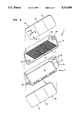
- FIG. 1 is a perspective representation generally illustrating the invention.
- FIG. 2 is a sectional view taken along line 2--2 in FIG. 1.
- FIG. 3 is an exploded view illustrating the components of the invention and the assembled relationship thereof to each other.
- FIG. 4 is a perspective view further illustrating the features of the invention.
- the packaging arrangement for power semiconductor devices includes a unitary case designated generally by the numeral 2. Case 2 is covered on opposite sides thereof by lids 4 and 6, for hermetically sealing the case. A cooling fluid inlet port is designated by the numeral 8 and a cooling fluid outlet port is designated by the numeral 10.
- case 2 has two sides 9 and 11, each of which has integral fins 16 and 18, respectively. Sides 9 and 11 are joined to form unitary case 2, whereby integral fins 16 and 18 cooperate to form a fin arrangement 19. Sides 9 and 11 are configured to provide heat sinks 13 and 15, respectively, as will be hereinafter more fully discussed. Cooling fluid enters one end of fin arrangement 19 via inlet port 8 (FIG. 1), flows over the fin arrangement, and exits the other end thereof via outlet port 10 (FIG. 1).
- case side 9 includes a base 24 and a continuous wall 28 extending peripherally around said base 24 on one surface thereof
- case side 11 includes a base 26 and a continuous wall 30 extending peripherally around said base 26 on one surface thereof.
- the surfaces of bases 24 and 26 surrounded by walls 28 and 30, respectively, are effective as heat sinks 13 and 15 (FIG. 2) as will be hereinafter referred to.
- Base side 9 includes longitudinally extending integral fins 18 on the surface thereof opposite wall 28 and base side 11 includes like extending integral fins 16 (shown in FIG. 2 but not otherwise shown in FIG. 3) on the surface thereof opposite wall 30.
- One side of wall 30 has holes such as 34 for accepting electrical feedthroughs from the circuitry enclosed in the package herein described.
- Fins 16 and 18 are transversely slotted via slots such as 17 for cooling fluid turbulence as particularly shown in FIG. 3 with relation to fins 18.
- Bases 24 and 26 carry holes 8A and 10A and 8B and 10B, respectively, which are aligned to provide ports 8 and 10 shown in FIG. 1.
- a plurality of members shown as three in number and designated by the numerals 36, 38 and 40 are suitably mounted to heat sink 13 (FIG. 2).
- a like plurality of members designated by the numerals 42, 44 and 46 are likewise suitably mounted to heat sink 15 (FIGS. 3 and 4).
- Members 36, 38, 40, 42, 44 and 46 are formed from a ceramic substrate with bonded metallic conductors mounted on both sides thereof.
- Power semiconductor circuits such as 47 which may include power semiconductor devices such as MOS-Controlled Thysistors (MCT's), are mounted on the metallic conductors so as to be conductively interconnected thereby.
- Case sides 9 and 11 are of a metal matrix composite (MMC) material.
- walls 28 and 30 are of a suitable metallic alloy such as Kovar.
- Feedthroughs such as 35 (FIG. 4) accepted in feedthrough holes 34 and connected to circuitry such as 47 are likewise of Kovar and are isolated from wall 30 by, for example, a pressure bonded glass seal.
- the metallic conductors bonded to the plurality of substrates to provide members 36, 38, 40, 42, 44 and 46 are of copper, whereby said members are soldered to the respective heat sinks.
- FIG. 4 The assembled configuration of the invention is best illustrated in FIG. 4. Sides 9 and 11 are metallurgically joined to provide a unitary case 2 (FIGS. 1 and 2). Lids 4 and 6 which are of the metal matrix composite material are mounted to the extending edges of walls 28 and 30, respectively, as by welding, whereby a hermetically sealed package can be provided, as is well known in the art.
- the metal matrix composite and ceramic substrate materials are selected so that their thermal coefficients of expansion (TCE's) are matched to provide a package suitable for the purposes intended.
- TCE's thermal coefficients of expansion
- the substrate material for components 36-46 is first selected and then the metal matrix composite material for case 2 and lids 4 and 6 is selected so that the respective TCE's match as closely as possible.
- a suitable ceramic substrate for members 36-46 has been found to be, for example, beryllia (beryllium oxide).
- a suitable metal matrix composite (MMC) material for case 2 and lids 4 and 6 has been found to be, for example, an aluminum/ceramic composite, i.e. a silicon carbide reinforced aluminum marketed by Lanxide Electronics Corp. of Newark, Del. under their trade designation PrimexTM.
- Other ceramics and MMC materials may be used as well, consistent with matching the respective TCE's as aforenoted.
Abstract
Description
Claims (13)
Priority Applications (1)
| Application Number | Priority Date | Filing Date | Title |
|---|---|---|---|
| US08/043,688 US5313098A (en) | 1993-04-08 | 1993-04-08 | Packaging arrangement for power semiconductor devices |
Applications Claiming Priority (1)
| Application Number | Priority Date | Filing Date | Title |
|---|---|---|---|
| US08/043,688 US5313098A (en) | 1993-04-08 | 1993-04-08 | Packaging arrangement for power semiconductor devices |
Publications (1)
| Publication Number | Publication Date |
|---|---|
| US5313098A true US5313098A (en) | 1994-05-17 |
Family
ID=21928380
Family Applications (1)
| Application Number | Title | Priority Date | Filing Date |
|---|---|---|---|
| US08/043,688 Expired - Lifetime US5313098A (en) | 1993-04-08 | 1993-04-08 | Packaging arrangement for power semiconductor devices |
Country Status (1)
| Country | Link |
|---|---|
| US (1) | US5313098A (en) |
Cited By (11)
| Publication number | Priority date | Publication date | Assignee | Title |
|---|---|---|---|---|
| US5480727A (en) * | 1994-02-03 | 1996-01-02 | Motorola, Inc. | Electronic device assembly and method for making |
| US5498907A (en) * | 1993-04-29 | 1996-03-12 | Allied Signal Inc. | Interconnection arrangement for power semiconductor switching devices |
| US5666269A (en) * | 1994-01-03 | 1997-09-09 | Motorola, Inc. | Metal matrix composite power dissipation apparatus |
| EP0798954A1 (en) * | 1996-03-26 | 1997-10-01 | Thomson-Csf | Microelectronic casing with cooling system |
| US5837556A (en) * | 1997-01-06 | 1998-11-17 | Sundstrand Corporation | Method of removing a component from a substrate |
| US5915463A (en) * | 1996-03-23 | 1999-06-29 | Motorola, Inc. | Heat dissipation apparatus and method |
| US6245442B1 (en) * | 1997-05-28 | 2001-06-12 | Kabushiki Kaisha Toyota Chuo | Metal matrix composite casting and manufacturing method thereof |
| US20030164206A1 (en) * | 2001-05-15 | 2003-09-04 | Cornie James A. | Discontinuous carbon fiber reinforced metal matrix composite |
| EP1358664A2 (en) * | 2001-01-31 | 2003-11-05 | Gentex Corporation | High power radiation emitter device and heat dissipating package for electronic components |
| US20060244118A1 (en) * | 2001-01-31 | 2006-11-02 | Gentex Corporation | High power radiation emitter device and heat dissipating package for electronic components |
| US7226809B2 (en) | 2002-06-18 | 2007-06-05 | Micron Technology, Inc. | Semiconductor devices and semiconductor device components with peripherally located, castellated contacts, assemblies and packages including such semiconductor devices or packages and associated methods |
Citations (3)
| Publication number | Priority date | Publication date | Assignee | Title |
|---|---|---|---|---|
| US4009423A (en) * | 1975-07-02 | 1977-02-22 | Honeywell Information Systems, Inc. | Liquid cooled heat exchanger for electronic power supplies |
| US5111280A (en) * | 1988-11-10 | 1992-05-05 | Iversen Arthur H | Thermal management of power conditioning systems |
| US5168348A (en) * | 1991-07-15 | 1992-12-01 | International Business Machines Corporation | Impingment cooled compliant heat sink |
-
1993
- 1993-04-08 US US08/043,688 patent/US5313098A/en not_active Expired - Lifetime
Patent Citations (3)
| Publication number | Priority date | Publication date | Assignee | Title |
|---|---|---|---|---|
| US4009423A (en) * | 1975-07-02 | 1977-02-22 | Honeywell Information Systems, Inc. | Liquid cooled heat exchanger for electronic power supplies |
| US5111280A (en) * | 1988-11-10 | 1992-05-05 | Iversen Arthur H | Thermal management of power conditioning systems |
| US5168348A (en) * | 1991-07-15 | 1992-12-01 | International Business Machines Corporation | Impingment cooled compliant heat sink |
Cited By (14)
| Publication number | Priority date | Publication date | Assignee | Title |
|---|---|---|---|---|
| US5498907A (en) * | 1993-04-29 | 1996-03-12 | Allied Signal Inc. | Interconnection arrangement for power semiconductor switching devices |
| US5666269A (en) * | 1994-01-03 | 1997-09-09 | Motorola, Inc. | Metal matrix composite power dissipation apparatus |
| US5480727A (en) * | 1994-02-03 | 1996-01-02 | Motorola, Inc. | Electronic device assembly and method for making |
| US5915463A (en) * | 1996-03-23 | 1999-06-29 | Motorola, Inc. | Heat dissipation apparatus and method |
| EP0798954A1 (en) * | 1996-03-26 | 1997-10-01 | Thomson-Csf | Microelectronic casing with cooling system |
| FR2747005A1 (en) * | 1996-03-26 | 1997-10-03 | Thomson Csf | MICROELECTRONIC PACKAGE WITH COOLING SYSTEM |
| US5837556A (en) * | 1997-01-06 | 1998-11-17 | Sundstrand Corporation | Method of removing a component from a substrate |
| US6245442B1 (en) * | 1997-05-28 | 2001-06-12 | Kabushiki Kaisha Toyota Chuo | Metal matrix composite casting and manufacturing method thereof |
| EP1358664A2 (en) * | 2001-01-31 | 2003-11-05 | Gentex Corporation | High power radiation emitter device and heat dissipating package for electronic components |
| US20060244118A1 (en) * | 2001-01-31 | 2006-11-02 | Gentex Corporation | High power radiation emitter device and heat dissipating package for electronic components |
| EP1358664A4 (en) * | 2001-01-31 | 2006-11-29 | Gentex Corp | High power radiation emitter device and heat dissipating package for electronic components |
| US7489031B2 (en) | 2001-01-31 | 2009-02-10 | Gentex Corporation | High power radiation emitter device and heat dissipating package for electronic components |
| US20030164206A1 (en) * | 2001-05-15 | 2003-09-04 | Cornie James A. | Discontinuous carbon fiber reinforced metal matrix composite |
| US7226809B2 (en) | 2002-06-18 | 2007-06-05 | Micron Technology, Inc. | Semiconductor devices and semiconductor device components with peripherally located, castellated contacts, assemblies and packages including such semiconductor devices or packages and associated methods |
Similar Documents
| Publication | Publication Date | Title |
|---|---|---|
| US5719444A (en) | Packaging and cooling system for power semi-conductor | |
| US6154369A (en) | Electronic assembly for removing heat from a semiconductor device | |
| US5792984A (en) | Molded aluminum nitride packages | |
| US5903583A (en) | Diode laser component with cooling element and diode laser module | |
| US4758926A (en) | Fluid-cooled integrated circuit package | |
| EP1378153B1 (en) | Electronic module including a cooling substrate and manufacturing method thereof | |
| US4764846A (en) | High density electronic package comprising stacked sub-modules | |
| US5250845A (en) | Totally enclosed hermetic electronic module | |
| US4860444A (en) | Method of assembling a fluid-cooled integrated circuit package | |
| US6060795A (en) | Semiconductor power pack | |
| US5313098A (en) | Packaging arrangement for power semiconductor devices | |
| US20100142150A1 (en) | Cooling apparatus with cold plate formed in situ on a surface to be cooled | |
| US6404048B2 (en) | Heat dissipating microelectronic package | |
| JPH05102362A (en) | Integrated radiator for semiconductor module | |
| EP1378154B1 (en) | Electronic module including a cooling substrate with fluid dissociation electrodes and operating method thereof | |
| US5565705A (en) | Electronic module for removing heat from a semiconductor die | |
| CN105870085B (en) | A kind of aluminium nitride multi-layer ceramics is without lead chip carrier encapsulation shell | |
| US5050036A (en) | Liquid cooled integrated circuit assembly | |
| WO1981003734A1 (en) | Heat pin integrated circuit packaging | |
| US3774078A (en) | Thermally integrated electronic assembly with tapered heat conductor | |
| CN111627875A (en) | High heat conduction heat abstractor | |
| WO2020210579A1 (en) | Microjet-cooled flanges for electronic devices | |
| US5942796A (en) | Package structure for high-power surface-mounted electronic devices | |
| EP0516875B1 (en) | Module for electronic package | |
| US5200640A (en) | Hermetic package having covers and a base providing for direct electrical connection |
Legal Events
| Date | Code | Title | Description |
|---|---|---|---|
| AS | Assignment |
Owner name: ALLIEDSIGNAL INC., NEW JERSEY Free format text: ASSIGNMENT OF ASSIGNORS INTEREST.;ASSIGNORS:TUMPEY, JOHN J.;BORDEN, RAYMOND W.;ECKENFELDER, ROBERT C.;AND OTHERS;REEL/FRAME:006519/0539 Effective date: 19930323 |
|
| STPP | Information on status: patent application and granting procedure in general |
Free format text: APPLICATION UNDERGOING PREEXAM PROCESSING |
|
| AS | Assignment |
Owner name: ALLIEDSIGNAL INC., NEW JERSEY Free format text: CHANGE OF NAME;ASSIGNOR:ALLIED-SIGNAL INC.;REEL/FRAME:006704/0091 Effective date: 19930426 |
|
| FEPP | Fee payment procedure |
Free format text: PAYOR NUMBER ASSIGNED (ORIGINAL EVENT CODE: ASPN); ENTITY STATUS OF PATENT OWNER: LARGE ENTITY |
|
| FPAY | Fee payment |
Year of fee payment: 4 |
|
| FPAY | Fee payment |
Year of fee payment: 8 |
|
| FPAY | Fee payment |
Year of fee payment: 12 |