US5319159A - Double-sided printed wiring board and method of manufacture thereof - Google Patents
Double-sided printed wiring board and method of manufacture thereof Download PDFInfo
- Publication number
- US5319159A US5319159A US07/991,553 US99155392A US5319159A US 5319159 A US5319159 A US 5319159A US 99155392 A US99155392 A US 99155392A US 5319159 A US5319159 A US 5319159A
- Authority
- US
- United States
- Prior art keywords
- hole
- base plate
- electrically conductive
- conductive layer
- printed wiring
- Prior art date
- Legal status (The legal status is an assumption and is not a legal conclusion. Google has not performed a legal analysis and makes no representation as to the accuracy of the status listed.)
- Expired - Fee Related
Links
Images


Classifications
-
- H—ELECTRICITY
- H05—ELECTRIC TECHNIQUES NOT OTHERWISE PROVIDED FOR
- H05K—PRINTED CIRCUITS; CASINGS OR CONSTRUCTIONAL DETAILS OF ELECTRIC APPARATUS; MANUFACTURE OF ASSEMBLAGES OF ELECTRICAL COMPONENTS
- H05K1/00—Printed circuits
- H05K1/02—Details
- H05K1/11—Printed elements for providing electric connections to or between printed circuits
- H05K1/111—Pads for surface mounting, e.g. lay-out
- H05K1/112—Pads for surface mounting, e.g. lay-out directly combined with via connections
- H05K1/113—Via provided in pad; Pad over filled via
-
- H—ELECTRICITY
- H05—ELECTRIC TECHNIQUES NOT OTHERWISE PROVIDED FOR
- H05K—PRINTED CIRCUITS; CASINGS OR CONSTRUCTIONAL DETAILS OF ELECTRIC APPARATUS; MANUFACTURE OF ASSEMBLAGES OF ELECTRICAL COMPONENTS
- H05K3/00—Apparatus or processes for manufacturing printed circuits
- H05K3/40—Forming printed elements for providing electric connections to or between printed circuits
- H05K3/42—Plated through-holes or plated via connections
- H05K3/425—Plated through-holes or plated via connections characterised by the sequence of steps for plating the through-holes or via connections in relation to the conductive pattern
- H05K3/427—Plated through-holes or plated via connections characterised by the sequence of steps for plating the through-holes or via connections in relation to the conductive pattern initial plating of through-holes in metal-clad substrates
-
- H—ELECTRICITY
- H05—ELECTRIC TECHNIQUES NOT OTHERWISE PROVIDED FOR
- H05K—PRINTED CIRCUITS; CASINGS OR CONSTRUCTIONAL DETAILS OF ELECTRIC APPARATUS; MANUFACTURE OF ASSEMBLAGES OF ELECTRICAL COMPONENTS
- H05K2201/00—Indexing scheme relating to printed circuits covered by H05K1/00
- H05K2201/03—Conductive materials
- H05K2201/0332—Structure of the conductor
- H05K2201/0335—Layered conductors or foils
- H05K2201/0347—Overplating, e.g. for reinforcing conductors or bumps; Plating over filled vias
-
- H—ELECTRICITY
- H05—ELECTRIC TECHNIQUES NOT OTHERWISE PROVIDED FOR
- H05K—PRINTED CIRCUITS; CASINGS OR CONSTRUCTIONAL DETAILS OF ELECTRIC APPARATUS; MANUFACTURE OF ASSEMBLAGES OF ELECTRICAL COMPONENTS
- H05K2201/00—Indexing scheme relating to printed circuits covered by H05K1/00
- H05K2201/09—Shape and layout
- H05K2201/09209—Shape and layout details of conductors
- H05K2201/095—Conductive through-holes or vias
- H05K2201/0959—Plated through-holes or plated blind vias filled with insulating material
-
- H—ELECTRICITY
- H05—ELECTRIC TECHNIQUES NOT OTHERWISE PROVIDED FOR
- H05K—PRINTED CIRCUITS; CASINGS OR CONSTRUCTIONAL DETAILS OF ELECTRIC APPARATUS; MANUFACTURE OF ASSEMBLAGES OF ELECTRICAL COMPONENTS
- H05K3/00—Apparatus or processes for manufacturing printed circuits
- H05K3/0094—Filling or covering plated through-holes or blind plated vias, e.g. for masking or for mechanical reinforcement
Definitions
- the present invention relates generally to printed wiring boards, and more particularly it relates to a double-sided printed wiring board on which semiconductor-based integrated circuits (referred hereinafter to as "ICs") may be mounted, and a process of manufacturing such double-sided printed wiring boards.
- ICs semiconductor-based integrated circuits
- a conventional printed wiring board carries ICs as well as other discrete electronic components and circuit elements, which are interconnected to provide the particular electronic circuit functions.
- those ICs, discrete electronic components and circuit elements are usually bonded to the printed wiring board via holes formed in the printed wiring board through which lead wires may be inserted and soldered to the board.
- surface mounting technology widely employed in the printed wiring board manufacturing field. This technology permits an IC to be mounted together with its associated elements on the printed wiring board without forming any through-holes in the board.
- ICs and other on-chip elements may be mounted on a chip land directly without using the through-holes.
- the appropriate through-via-holes must be provided remotely from the chip land, and any wiring pattern required for interconnecting the elements via the through-via-holes must be formed on the surface of the base plate.
- the chip land and through-via-holes must be provided at different locations on the printed wiring board.
- a corresponding reduction in the size of the chip land is required so that they can be mounted on the chip land.
- the wiring pattern that includes leads drawn out from the chip land and distributed across different locations must be accordingly fine, but technically, this is practically difficult to achieve. It is also difficult to secure the space required for wiring the leads. In particular, for a double-sided high-density wiring pattern implementation, this space limitation poses a problem.
- the through-via-holes formed in the printed wiring board are exposed on each of the opposite sides of the board.
- the principal object of the present invention is to solve the prior art problems as described above. According to the present invention, it is possible to eliminate the need of forming the wiring pattern on either of the opposite sides of a printed wiring board that is required in the prior art for interconnecting the chip land and through-via-holes.
- Another object of the present invention is therefore to provide a double-sided printed wiring board that achieves the above object, and to provide a method of manufacture thereof whereby such a double-sided printed wiring board can be manufactured to achieve the above same object.
- Another object of the present invention is to provide a double-sided printed wiring board and a method of manufacture thereof wherein through-via-holes are provided in such a way that no surplus solder can overflow through the through-via-holes.
- the double-sided printed wiring board of the present invention includes a base plate having a wiring pattern printed on each of the opposite sides thereof, at least one of the opposite sides having a chip land formed thereon.
- the chip extends directly over a through-via-hole which is filled with any suitable synthetic resin.
- the chip land that has been described above covers the synthetic resin filling and solidified in the particular through-via-hole.
- the synthetic resin filler that has been solidified may be flattened to be flush with the plane of the through-via-hole by removing or planing any surplus resin that is forced out from the exposed ends of the hole.
- the present invention also provides a method of manufacturing such a double-sided printed wiring board, including a sequence of steps as follows:
- Plating the inside of the through-via-holes and plating the copper foil-laminated base plate on its opposite sides may be accomplished by a non-electrolytic copper plating process, followed by an electrolytic copper plating process.
- the synthetic resin that has filled and has been solidified in the particular through-via-hole may have been forced out of the through-via-hole.
- any surplus resin that exists outside the hole may preferably be removed so that it can be flush with the plane of the exposed end of the hole.
- the copper foil-laminated plate includes copper foils on the opposite sides thereof which constitute a double-sided printed wiring board. It may comprise a base plate such as paper, glass or the like that provides the support, any synthetic resin such as phenol, polyester, epoxy, polyimide, teflon (trademark), polysulfone, fluorine, and other similar resins that are capable of fixing the support, and copper foils that are used for making wiring patterns.
- a base plate such as paper, glass or the like that provides the support
- any synthetic resin such as phenol, polyester, epoxy, polyimide, teflon (trademark), polysulfone, fluorine, and other similar resins that are capable of fixing the support, and copper foils that are used for making wiring patterns.
- a suitable resin in the through-via-holes there are several methods of providing a suitable resin in the through-via-holes.
- One example is the screen printing method.
- Another example is a thermal bonding process using a press.
- a base sheet such as a glass cloth and the like is impregnated with any suitable resin, and the resin-impregnated base sheet is formed into a sheet called a prepreg by hardening it thermally until the impregnated resin assumes a half-hardened state.
- a single or several sheets of prepreg are inserted into the through-via-hole, and are then thermally bonded to the through-via-hole by using the press.
- the screen printing process is preferred because it requires no complicated equipment such as that used for the thermal bonding process.
- the resin that is used with the screen printing process should preferably contain less solvent, specifically less than 10% of solvent.
- the present invention eliminates the need of providing the wiring pattern specifically intended for the interconnection between the chip land and the corresponding through-via-hole.
- the closed through-via-hole that is obtained by filling the through-via-hole with the resin prevents any extra solder from overflowing when dipping the board in a solder bath.
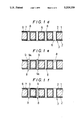
- FIG. 1a through FIG. 1i represent the different stages of the manufacturing process according to the preferred embodiment of the present invention, depicting how a double-sided printed wiring board which is shown in an enlarged sectional view is being fabricated through each succeeding stage;
- FIG. 2 is a schematic representation showing a chip land and other patterns in plan.
- FIG. 1a through FIG. 1i the steps of completing a printed wiring board according to the present invention will be described.
- a base plate 1 which is 1 mm thick is formed to a square shape having the size of 340 mm ⁇ 340 mm. Then, a copper foil 2 which is 18 ⁇ m thick is laminated onto each of the opposite sides of the base plate 1. A copper foil laminated board 3 is thus obtained. Next, a plurality of through-holes 4, 4 each having a diameter of 0.3 mm are formed in the copper foil laminated board 3, and a plurality of holes 5, 5 each having a diameter of 0.8 mm are also formed (FIG. 1b). The holes 5, 5 are provided for accommodating a lead wire of electronic components therein.
- the copper foil-laminated board 3 that has the through-holes 4, 4 and the component holes 5, 5 formed therein as described above goes through a non-electrolytic copper plating process during which a non-electrolytic copper layer 6 is plated on the opposite sides of the board 3, and on the internal walls of the board defining the through-holes 4, 4 and component holes 5, 5, respectively (FIG. 1c).
- the resulting layer 6 is 0.4 ⁇ m thick.
- an electrolytic copper plating process during which an electrolytic copper layer 7 is plated on the layer 6 at each part of the board 3 (FIG. 1d).
- the resulting layer 7 is 25 ⁇ m thick.
- an epoxy resin 9 fills some of the through-via-holes 8 and is allowed to solidify (FIG. 1e).
- the epoxy resin 9 that may be used in the screen printing may contain 2.3% of hydrocarbon selected from those elements in the aromatic group, and may be allowed to solidify under 130° C. heat applied for 30 minutes.
- the copper foil laminated board 3 having the original (open) through-via-holes 8 and the filled (closed) through-holes formed during the preceding steps is again subjected to a non-electrolytic copper plating process, followed by another electrolytic copper plating process.
- a non-electrolytic copper layer 10 is first plated (FIG. 1g), and an electrolytic copper layer 11 is then plated on the layer 11 (FIG. 1h).
- a light-sensitive drum film 13 is thermally laminated on the board 3, and only those portions of the board 3 which are required to be exposed are exposed to ultraviolet rays in a process such as a subtractive process. The remaining portions not exposed are removed during a development process.
- the copper-plated portions are etched with a solution of ferric chloride.
- signal lines 12 are formed, and a chip land 13 is formed on the filled through-via-holes 8 (FIG. 1i).
- FIG. 2 depicts the chip land 13, signal line 12, and the pattern 14 aligned with an open through-via-hole 8 as well as a pattern 15 aligned with a closed through-via-hole 8.
- the double-sided printed wiring board described above allows the chip land 13 and the pattern on the opposite side to be electrically conductively interconnected via the closed through-via-hole 8. This eliminates the need of providing a through-via-hole remotely from the chip land 13, and therefore it is not necessary to implement a wiring pattern to interconnect the chip land to a remote through-hole. Thus, a high-density packing can be realized.
- the wiring pattern required to interconnect the chip land and the corresponding through-via-hole can be eliminated, and the space thus made available on the double-sided printed wiring board can be utilized for wiring the signal lines.
- the space can be better utilized so that high-density wiring can be achieved.
- the present invention allows for greater flexibility in designing the signal wiring pattern, which can easily be done on a CAD-implemented workstation or personal computer.
- the present invention prevents any surplus solder from overflowing when an electronic component is soldered to the hole.
- ICs and other electronic or circuit components may be mounted on the printed wiring board without difficulty, and higher reliability can be achieved.
Abstract
Description
Claims (5)
Priority Applications (1)
| Application Number | Priority Date | Filing Date | Title |
|---|---|---|---|
| US07/991,553 US5319159A (en) | 1992-12-15 | 1992-12-15 | Double-sided printed wiring board and method of manufacture thereof |
Applications Claiming Priority (1)
| Application Number | Priority Date | Filing Date | Title |
|---|---|---|---|
| US07/991,553 US5319159A (en) | 1992-12-15 | 1992-12-15 | Double-sided printed wiring board and method of manufacture thereof |
Publications (1)
| Publication Number | Publication Date |
|---|---|
| US5319159A true US5319159A (en) | 1994-06-07 |
Family
ID=25537322
Family Applications (1)
| Application Number | Title | Priority Date | Filing Date |
|---|---|---|---|
| US07/991,553 Expired - Fee Related US5319159A (en) | 1992-12-15 | 1992-12-15 | Double-sided printed wiring board and method of manufacture thereof |
Country Status (1)
| Country | Link |
|---|---|
| US (1) | US5319159A (en) |
Cited By (31)
| Publication number | Priority date | Publication date | Assignee | Title |
|---|---|---|---|---|
| EP0713359A1 (en) * | 1994-11-21 | 1996-05-22 | International Business Machines Corporation | Printed circuit boards with selectively filled plated through holes |
| US5539181A (en) * | 1992-08-26 | 1996-07-23 | International Business Machines Corporation | Circuit board |
| US5541368A (en) * | 1994-07-15 | 1996-07-30 | Dell Usa, L.P. | Laminated multi chip module interconnect apparatus |
| GB2307351A (en) * | 1995-11-16 | 1997-05-21 | Marconi Gec Ltd | Printed circuit boards and their manufacture |
| US5689091A (en) * | 1996-09-19 | 1997-11-18 | Vlsi Technology, Inc. | Multi-layer substrate structure |
| US5822856A (en) * | 1996-06-28 | 1998-10-20 | International Business Machines Corporation | Manufacturing circuit board assemblies having filled vias |
| US6090474A (en) * | 1998-09-01 | 2000-07-18 | International Business Machines Corporation | Flowable compositions and use in filling vias and plated through-holes |
| EP1063699A1 (en) * | 1998-02-10 | 2000-12-27 | Nissha Printing Co., Ltd. | Base sheet for semiconductor module, method for manufacturing base sheet for semiconductor module, and semiconductor module |
| US6204455B1 (en) * | 1995-07-31 | 2001-03-20 | Tessera, Inc. | Microelectronic component mounting with deformable shell terminals |
| US6297458B1 (en) * | 1999-04-14 | 2001-10-02 | Dell Usa, L.P. | Printed circuit board and method for evaluating the inner layer hole registration process capability of the printed circuit board manufacturing process |
| US6303881B1 (en) | 1998-03-20 | 2001-10-16 | Viasystems, Inc. | Via connector and method of making same |
| US6365844B2 (en) * | 1997-08-20 | 2002-04-02 | Matsushita Electric Industrial Co., Ltd. | Printed wiring board |
| EP1197131A1 (en) * | 1999-03-29 | 2002-04-17 | Viasystems, Inc. | A via connector and method of making same |
| US6423906B2 (en) * | 1999-09-21 | 2002-07-23 | Youngtek Electronics Corp. | Surface mount package for long lead devices |
| US6452117B2 (en) * | 1999-08-26 | 2002-09-17 | International Business Machines Corporation | Method for filling high aspect ratio via holes in electronic substrates and the resulting holes |
| US6486414B2 (en) * | 2000-09-07 | 2002-11-26 | International Business Machines Corporation | Through-hole structure and printed circuit board including the through-hole structure |
| US6485892B1 (en) | 1999-12-17 | 2002-11-26 | International Business Machines Corporation | Method for masking a hole in a substrate during plating |
| US6518515B2 (en) | 1999-02-10 | 2003-02-11 | Matsushita Electric Industrial Co, Ltd. | Printed wiring board, and method and apparatus for manufacturing the same |
| US20030034175A1 (en) * | 2001-08-20 | 2003-02-20 | Honeywell Advanced Circuits, Inc. | Configurations and methods for improved copper distribution uniformity in printed wiring boards |
| US6598291B2 (en) | 1998-03-20 | 2003-07-29 | Viasystems, Inc. | Via connector and method of making same |
| US20040141299A1 (en) * | 1999-04-29 | 2004-07-22 | Unicap Electronics Industrial Corporation | Burrless castellation via process and product for plastic chip carrier |
| US20040173890A1 (en) * | 2000-07-27 | 2004-09-09 | Fujitsu Limited | Front-and-back electrically conductive substrate and method for manufacturing same |
| US6982387B2 (en) * | 2001-06-19 | 2006-01-03 | International Business Machines Corporation | Method and apparatus to establish circuit layers interconnections |
| US20060219428A1 (en) * | 2005-03-29 | 2006-10-05 | Hitachi Cable, Ltd. | Double-sided wiring board fabrication method, double-sided wiring board, and base material therefor |
| US20070017693A1 (en) * | 2005-07-25 | 2007-01-25 | Bois Karl J | Printed circuit board including pads with vacancies |
| US7417867B1 (en) | 1999-09-27 | 2008-08-26 | Sony Corporation | Printed wiring board and display apparatus |
| US20110292296A1 (en) * | 2010-05-31 | 2011-12-01 | Kenji Hasegawa | Television apparatus, electronic device, and circuit board structure |
| US20120144667A1 (en) * | 2007-06-06 | 2012-06-14 | Ddi Global Corp. | Multilayer printed wiring boards with holes requiring copper wrap plate |
| US20130220675A1 (en) * | 2007-02-20 | 2013-08-29 | Rajwant Sidhu | Method of manufacturing a printed circuit board |
| US20130313010A1 (en) * | 2012-05-28 | 2013-11-28 | Shinko Electric Industries Co., Ltd. | Wiring board and method of manufacturing the same |
| US20160150635A1 (en) * | 2014-11-21 | 2016-05-26 | HongQiSheng Precision Electronics (QinHuanDao) Co., Ltd. | Flexible printed circuit board and method for manufacturing same |
Citations (7)
| Publication number | Priority date | Publication date | Assignee | Title |
|---|---|---|---|---|
| US4659931A (en) * | 1985-05-08 | 1987-04-21 | Grumman Aerospace Corporation | High density multi-layered integrated circuit package |
| JPS6338878A (en) * | 1986-07-31 | 1988-02-19 | 株式会社 ウロコ製作所 | Drier |
| US4791248A (en) * | 1987-01-22 | 1988-12-13 | The Boeing Company | Printed wire circuit board and its method of manufacture |
| JPS6424491A (en) * | 1987-07-21 | 1989-01-26 | Canon Kk | Printed board |
| JPS6429868A (en) * | 1987-07-24 | 1989-01-31 | Mita Industrial Co Ltd | Controller for copying machine with document feeding means |
| JPH01143292A (en) * | 1987-11-27 | 1989-06-05 | Matsushita Electric Ind Co Ltd | Manufacture of printed wiring board |
| JPH02134895A (en) * | 1988-11-16 | 1990-05-23 | Fujitsu Ltd | Connection land of surface mounting type component |
-
1992
- 1992-12-15 US US07/991,553 patent/US5319159A/en not_active Expired - Fee Related
Patent Citations (7)
| Publication number | Priority date | Publication date | Assignee | Title |
|---|---|---|---|---|
| US4659931A (en) * | 1985-05-08 | 1987-04-21 | Grumman Aerospace Corporation | High density multi-layered integrated circuit package |
| JPS6338878A (en) * | 1986-07-31 | 1988-02-19 | 株式会社 ウロコ製作所 | Drier |
| US4791248A (en) * | 1987-01-22 | 1988-12-13 | The Boeing Company | Printed wire circuit board and its method of manufacture |
| JPS6424491A (en) * | 1987-07-21 | 1989-01-26 | Canon Kk | Printed board |
| JPS6429868A (en) * | 1987-07-24 | 1989-01-31 | Mita Industrial Co Ltd | Controller for copying machine with document feeding means |
| JPH01143292A (en) * | 1987-11-27 | 1989-06-05 | Matsushita Electric Ind Co Ltd | Manufacture of printed wiring board |
| JPH02134895A (en) * | 1988-11-16 | 1990-05-23 | Fujitsu Ltd | Connection land of surface mounting type component |
Cited By (47)
| Publication number | Priority date | Publication date | Assignee | Title |
|---|---|---|---|---|
| US5539181A (en) * | 1992-08-26 | 1996-07-23 | International Business Machines Corporation | Circuit board |
| US5541368A (en) * | 1994-07-15 | 1996-07-30 | Dell Usa, L.P. | Laminated multi chip module interconnect apparatus |
| EP0713359A1 (en) * | 1994-11-21 | 1996-05-22 | International Business Machines Corporation | Printed circuit boards with selectively filled plated through holes |
| US6204455B1 (en) * | 1995-07-31 | 2001-03-20 | Tessera, Inc. | Microelectronic component mounting with deformable shell terminals |
| GB2307351A (en) * | 1995-11-16 | 1997-05-21 | Marconi Gec Ltd | Printed circuit boards and their manufacture |
| US6178093B1 (en) | 1996-06-28 | 2001-01-23 | International Business Machines Corporation | Information handling system with circuit assembly having holes filled with filler material |
| US6000129A (en) * | 1996-06-28 | 1999-12-14 | International Business Machines Corporation | Process for manufacturing a circuit with filled holes |
| US6114019A (en) * | 1996-06-28 | 2000-09-05 | International Business Machines Corporation | Circuit board assemblies having filled vias free from bleed-out |
| US6127025A (en) * | 1996-06-28 | 2000-10-03 | International Business Machines Corporation | Circuit board with wiring sealing filled holes |
| US6138350A (en) * | 1996-06-28 | 2000-10-31 | International Business Machines Corporation | Process for manufacturing a circuit board with filled holes |
| US5822856A (en) * | 1996-06-28 | 1998-10-20 | International Business Machines Corporation | Manufacturing circuit board assemblies having filled vias |
| US5689091A (en) * | 1996-09-19 | 1997-11-18 | Vlsi Technology, Inc. | Multi-layer substrate structure |
| US6365844B2 (en) * | 1997-08-20 | 2002-04-02 | Matsushita Electric Industrial Co., Ltd. | Printed wiring board |
| EP1063699A1 (en) * | 1998-02-10 | 2000-12-27 | Nissha Printing Co., Ltd. | Base sheet for semiconductor module, method for manufacturing base sheet for semiconductor module, and semiconductor module |
| EP1063699A4 (en) * | 1998-02-10 | 2007-07-25 | Nissha Printing | Base sheet for semiconductor module, method for manufacturing base sheet for semiconductor module, and semiconductor module |
| US6303881B1 (en) | 1998-03-20 | 2001-10-16 | Viasystems, Inc. | Via connector and method of making same |
| US6598291B2 (en) | 1998-03-20 | 2003-07-29 | Viasystems, Inc. | Via connector and method of making same |
| US6090474A (en) * | 1998-09-01 | 2000-07-18 | International Business Machines Corporation | Flowable compositions and use in filling vias and plated through-holes |
| US6518515B2 (en) | 1999-02-10 | 2003-02-11 | Matsushita Electric Industrial Co, Ltd. | Printed wiring board, and method and apparatus for manufacturing the same |
| US6671951B2 (en) * | 1999-02-10 | 2004-01-06 | Matsushita Electric Industrial Co., Ltd. | Printed wiring board, and method and apparatus for manufacturing the same |
| EP1197131A4 (en) * | 1999-03-29 | 2006-07-19 | Viasystems Inc | A via connector and method of making same |
| EP1197131A1 (en) * | 1999-03-29 | 2002-04-17 | Viasystems, Inc. | A via connector and method of making same |
| US6297458B1 (en) * | 1999-04-14 | 2001-10-02 | Dell Usa, L.P. | Printed circuit board and method for evaluating the inner layer hole registration process capability of the printed circuit board manufacturing process |
| US20040141299A1 (en) * | 1999-04-29 | 2004-07-22 | Unicap Electronics Industrial Corporation | Burrless castellation via process and product for plastic chip carrier |
| US6452117B2 (en) * | 1999-08-26 | 2002-09-17 | International Business Machines Corporation | Method for filling high aspect ratio via holes in electronic substrates and the resulting holes |
| US6423906B2 (en) * | 1999-09-21 | 2002-07-23 | Youngtek Electronics Corp. | Surface mount package for long lead devices |
| US7417867B1 (en) | 1999-09-27 | 2008-08-26 | Sony Corporation | Printed wiring board and display apparatus |
| US6485892B1 (en) | 1999-12-17 | 2002-11-26 | International Business Machines Corporation | Method for masking a hole in a substrate during plating |
| US7579553B2 (en) * | 2000-07-27 | 2009-08-25 | Fujitsu Limited | Front-and-back electrically conductive substrate |
| US20040173890A1 (en) * | 2000-07-27 | 2004-09-09 | Fujitsu Limited | Front-and-back electrically conductive substrate and method for manufacturing same |
| US7222420B2 (en) | 2000-07-27 | 2007-05-29 | Fujitsu Limited | Method for making a front and back conductive substrate |
| US6486414B2 (en) * | 2000-09-07 | 2002-11-26 | International Business Machines Corporation | Through-hole structure and printed circuit board including the through-hole structure |
| US6982387B2 (en) * | 2001-06-19 | 2006-01-03 | International Business Machines Corporation | Method and apparatus to establish circuit layers interconnections |
| US20030034175A1 (en) * | 2001-08-20 | 2003-02-20 | Honeywell Advanced Circuits, Inc. | Configurations and methods for improved copper distribution uniformity in printed wiring boards |
| US7681310B2 (en) * | 2005-03-29 | 2010-03-23 | Hitachi Cable, Ltd. | Method for fabricating double-sided wiring board |
| US20060219428A1 (en) * | 2005-03-29 | 2006-10-05 | Hitachi Cable, Ltd. | Double-sided wiring board fabrication method, double-sided wiring board, and base material therefor |
| US7238892B2 (en) * | 2005-07-25 | 2007-07-03 | Hewlett-Packard Development Company, L.P. | Printed circuit board including pads with vacancies |
| US20070017693A1 (en) * | 2005-07-25 | 2007-01-25 | Bois Karl J | Printed circuit board including pads with vacancies |
| US20130220675A1 (en) * | 2007-02-20 | 2013-08-29 | Rajwant Sidhu | Method of manufacturing a printed circuit board |
| US20120144667A1 (en) * | 2007-06-06 | 2012-06-14 | Ddi Global Corp. | Multilayer printed wiring boards with holes requiring copper wrap plate |
| US8510941B2 (en) * | 2007-06-06 | 2013-08-20 | Ddi Global Corp. | Methods of manufacturing a printed wiring board having copper wrap plated hole |
| US20110292296A1 (en) * | 2010-05-31 | 2011-12-01 | Kenji Hasegawa | Television apparatus, electronic device, and circuit board structure |
| US8513538B2 (en) * | 2010-05-31 | 2013-08-20 | Kabushiki Kaisha Toshiba | Television apparatus, electronic device, and circuit board structure |
| US20130313010A1 (en) * | 2012-05-28 | 2013-11-28 | Shinko Electric Industries Co., Ltd. | Wiring board and method of manufacturing the same |
| US9232641B2 (en) * | 2012-05-28 | 2016-01-05 | Shinko Electric Industries Co., Ltd. | Wiring board and method of manufacturing the same |
| US20160150635A1 (en) * | 2014-11-21 | 2016-05-26 | HongQiSheng Precision Electronics (QinHuanDao) Co., Ltd. | Flexible printed circuit board and method for manufacturing same |
| US10285260B2 (en) * | 2014-11-21 | 2019-05-07 | Avary Holding (Shenzhen) Co., Limited. | Flexible printed circuit board and method for manufacturing same |
Similar Documents
| Publication | Publication Date | Title |
|---|---|---|
| US5319159A (en) | Double-sided printed wiring board and method of manufacture thereof | |
| EP0478313B1 (en) | A multilayer printed circuit board and manufacturing method therefor | |
| US4591411A (en) | Method for forming a high density printed wiring board | |
| US4663497A (en) | High density printed wiring board | |
| US5428190A (en) | Rigid-flex board with anisotropic interconnect and method of manufacture | |
| US6531661B2 (en) | Multilayer printed circuit board and method of making the same | |
| KR100268742B1 (en) | A method for forming metallized patterns on the top surface of a printed circuit board | |
| US6687985B2 (en) | Method of Manufacturing a multi-layer circuit board | |
| GB2313713A (en) | High-density mounting method for and structure of electronic circuit board | |
| KR970023931A (en) | Circuit board and manufacturing method thereof, bump type contact head using the circuit board, and semiconductor component mounting module | |
| KR20170037331A (en) | Printed circuit board and method for manufacturing the same | |
| US4720915A (en) | Printed circuit board and process for its manufacture | |
| US6009620A (en) | Method of making a printed circuit board having filled holes | |
| US3344515A (en) | Multilayer laminated wiring | |
| US3219749A (en) | Multilayer printed circuit board with solder access apertures | |
| US6651324B1 (en) | Process for manufacture of printed circuit boards with thick copper power circuitry and thin copper signal circuitry on the same layer | |
| US6256874B1 (en) | Conductor interconnect with dendrites through film and method for producing same | |
| KR100972431B1 (en) | Embedded printed circuit board and manufacturing method thereof | |
| US6594893B2 (en) | Method of making surface laminar circuit board | |
| KR101067214B1 (en) | A printed circuit board and a method of manufacturing the same | |
| JP2548584B2 (en) | Method for manufacturing circuit board with solder bumps | |
| EP0275686A1 (en) | Improved multi-layer printed circuit boards, and methods of manufacturing such boards | |
| US6492007B1 (en) | Multi-layer printed circuit bare board enabling higher density wiring and a method of manufacturing the same | |
| EP0108116B1 (en) | High density printed wiring board | |
| US4847446A (en) | Printed circuit boards and method for manufacturing printed circuit boards |
Legal Events
| Date | Code | Title | Description |
|---|---|---|---|
| AS | Assignment |
Owner name: YKC CORPORATION, JAPAN Free format text: ASSIGNMENT OF ASSIGNORS INTEREST.;ASSIGNORS:WATANABE, KOUICHI;FURUHASHI, ISAO;REEL/FRAME:006367/0838 Effective date: 19921208 Owner name: SONY CORPORATION, JAPAN Free format text: ASSIGNMENT OF ASSIGNORS INTEREST.;ASSIGNORS:WATANABE, KOUICHI;FURUHASHI, ISAO;REEL/FRAME:006367/0838 Effective date: 19921208 |
|
| FPAY | Fee payment |
Year of fee payment: 4 |
|
| FPAY | Fee payment |
Year of fee payment: 8 |
|
| REMI | Maintenance fee reminder mailed | ||
| LAPS | Lapse for failure to pay maintenance fees | ||
| STCH | Information on status: patent discontinuation |
Free format text: PATENT EXPIRED DUE TO NONPAYMENT OF MAINTENANCE FEES UNDER 37 CFR 1.362 |
|
| FP | Lapsed due to failure to pay maintenance fee |
Effective date: 20060607 |