US5323020A - High performance MESFET with multiple quantum wells - Google Patents
High performance MESFET with multiple quantum wells Download PDFInfo
- Publication number
- US5323020A US5323020A US07/995,459 US99545992A US5323020A US 5323020 A US5323020 A US 5323020A US 99545992 A US99545992 A US 99545992A US 5323020 A US5323020 A US 5323020A
- Authority
- US
- United States
- Prior art keywords
- region
- fet
- channel
- gate
- source
- Prior art date
- Legal status (The legal status is an assumption and is not a legal conclusion. Google has not performed a legal analysis and makes no representation as to the accuracy of the status listed.)
- Expired - Lifetime
Links
- XUIMIQQOPSSXEZ-UHFFFAOYSA-N Silicon Chemical compound [Si] XUIMIQQOPSSXEZ-UHFFFAOYSA-N 0.000 claims abstract description 29
- 229910052710 silicon Inorganic materials 0.000 claims abstract description 29
- 239000010703 silicon Substances 0.000 claims abstract description 29
- 239000002019 doping agent Substances 0.000 claims abstract description 26
- 239000004065 semiconductor Substances 0.000 claims abstract description 17
- 239000000758 substrate Substances 0.000 claims abstract description 14
- 229910052751 metal Inorganic materials 0.000 claims abstract description 8
- 239000002184 metal Substances 0.000 claims abstract description 8
- 229910000577 Silicon-germanium Inorganic materials 0.000 claims abstract description 7
- 230000005669 field effect Effects 0.000 claims abstract description 7
- 239000000463 material Substances 0.000 claims description 9
- 230000007423 decrease Effects 0.000 claims description 6
- VYPSYNLAJGMNEJ-UHFFFAOYSA-N Silicium dioxide Chemical compound O=[Si]=O VYPSYNLAJGMNEJ-UHFFFAOYSA-N 0.000 claims description 4
- 229910052732 germanium Inorganic materials 0.000 claims description 4
- GNPVGFCGXDBREM-UHFFFAOYSA-N germanium atom Chemical compound [Ge] GNPVGFCGXDBREM-UHFFFAOYSA-N 0.000 claims description 4
- 229910052681 coesite Inorganic materials 0.000 claims description 2
- 229910052906 cristobalite Inorganic materials 0.000 claims description 2
- 229910052594 sapphire Inorganic materials 0.000 claims description 2
- 239000010980 sapphire Substances 0.000 claims description 2
- 239000000377 silicon dioxide Substances 0.000 claims description 2
- 229910052682 stishovite Inorganic materials 0.000 claims description 2
- 229910052905 tridymite Inorganic materials 0.000 claims description 2
- 230000005684 electric field Effects 0.000 abstract 1
- 108091006146 Channels Proteins 0.000 description 72
- 238000000034 method Methods 0.000 description 8
- JBRZTFJDHDCESZ-UHFFFAOYSA-N AsGa Chemical compound [As]#[Ga] JBRZTFJDHDCESZ-UHFFFAOYSA-N 0.000 description 6
- 229910001218 Gallium arsenide Inorganic materials 0.000 description 5
- 230000002829 reductive effect Effects 0.000 description 5
- 230000000694 effects Effects 0.000 description 4
- 230000006872 improvement Effects 0.000 description 4
- 238000005468 ion implantation Methods 0.000 description 3
- 238000010884 ion-beam technique Methods 0.000 description 3
- 230000000873 masking effect Effects 0.000 description 3
- 238000012545 processing Methods 0.000 description 3
- 238000013459 approach Methods 0.000 description 2
- 230000003247 decreasing effect Effects 0.000 description 2
- 238000010586 diagram Methods 0.000 description 2
- 238000005516 engineering process Methods 0.000 description 2
- 238000000407 epitaxy Methods 0.000 description 2
- 239000007943 implant Substances 0.000 description 2
- 238000002513 implantation Methods 0.000 description 2
- 239000012535 impurity Substances 0.000 description 2
- 238000004519 manufacturing process Methods 0.000 description 2
- 238000001451 molecular beam epitaxy Methods 0.000 description 2
- 230000008569 process Effects 0.000 description 2
- ZAMOUSCENKQFHK-UHFFFAOYSA-N Chlorine atom Chemical compound [Cl] ZAMOUSCENKQFHK-UHFFFAOYSA-N 0.000 description 1
- 102000004129 N-Type Calcium Channels Human genes 0.000 description 1
- 108090000699 N-Type Calcium Channels Proteins 0.000 description 1
- 208000012868 Overgrowth Diseases 0.000 description 1
- 230000004888 barrier function Effects 0.000 description 1
- 230000015556 catabolic process Effects 0.000 description 1
- 238000005229 chemical vapour deposition Methods 0.000 description 1
- 229910052801 chlorine Inorganic materials 0.000 description 1
- 239000000460 chlorine Substances 0.000 description 1
- 238000010276 construction Methods 0.000 description 1
- 238000007796 conventional method Methods 0.000 description 1
- 230000007547 defect Effects 0.000 description 1
- 230000001934 delay Effects 0.000 description 1
- 238000009826 distribution Methods 0.000 description 1
- 230000005686 electrostatic field Effects 0.000 description 1
- 238000005530 etching Methods 0.000 description 1
- 230000010365 information processing Effects 0.000 description 1
- 239000011810 insulating material Substances 0.000 description 1
- 238000001459 lithography Methods 0.000 description 1
- 238000001465 metallisation Methods 0.000 description 1
- 239000000203 mixture Substances 0.000 description 1
- 238000012986 modification Methods 0.000 description 1
- 230000004048 modification Effects 0.000 description 1
- 230000003071 parasitic effect Effects 0.000 description 1
- 230000001681 protective effect Effects 0.000 description 1
- 238000004151 rapid thermal annealing Methods 0.000 description 1
- 230000009467 reduction Effects 0.000 description 1
- 230000004044 response Effects 0.000 description 1
- 230000002441 reversible effect Effects 0.000 description 1
- 238000000926 separation method Methods 0.000 description 1
- 238000005245 sintering Methods 0.000 description 1
- 238000002207 thermal evaporation Methods 0.000 description 1
Images


Classifications
-
- H—ELECTRICITY
- H01—ELECTRIC ELEMENTS
- H01L—SEMICONDUCTOR DEVICES NOT COVERED BY CLASS H10
- H01L29/00—Semiconductor devices adapted for rectifying, amplifying, oscillating or switching, or capacitors or resistors with at least one potential-jump barrier or surface barrier, e.g. PN junction depletion layer or carrier concentration layer; Details of semiconductor bodies or of electrodes thereof ; Multistep manufacturing processes therefor
- H01L29/66—Types of semiconductor device ; Multistep manufacturing processes therefor
- H01L29/68—Types of semiconductor device ; Multistep manufacturing processes therefor controllable by only the electric current supplied, or only the electric potential applied, to an electrode which does not carry the current to be rectified, amplified or switched
- H01L29/76—Unipolar devices, e.g. field effect transistors
- H01L29/772—Field effect transistors
- H01L29/80—Field effect transistors with field effect produced by a PN or other rectifying junction gate, i.e. potential-jump barrier
- H01L29/808—Field effect transistors with field effect produced by a PN or other rectifying junction gate, i.e. potential-jump barrier with a PN junction gate, e.g. PN homojunction gate
- H01L29/8086—Thin film JFET's
-
- H—ELECTRICITY
- H01—ELECTRIC ELEMENTS
- H01L—SEMICONDUCTOR DEVICES NOT COVERED BY CLASS H10
- H01L29/00—Semiconductor devices adapted for rectifying, amplifying, oscillating or switching, or capacitors or resistors with at least one potential-jump barrier or surface barrier, e.g. PN junction depletion layer or carrier concentration layer; Details of semiconductor bodies or of electrodes thereof ; Multistep manufacturing processes therefor
- H01L29/02—Semiconductor bodies ; Multistep manufacturing processes therefor
- H01L29/06—Semiconductor bodies ; Multistep manufacturing processes therefor characterised by their shape; characterised by the shapes, relative sizes, or dispositions of the semiconductor regions ; characterised by the concentration or distribution of impurities within semiconductor regions
- H01L29/10—Semiconductor bodies ; Multistep manufacturing processes therefor characterised by their shape; characterised by the shapes, relative sizes, or dispositions of the semiconductor regions ; characterised by the concentration or distribution of impurities within semiconductor regions with semiconductor regions connected to an electrode not carrying current to be rectified, amplified or switched and such electrode being part of a semiconductor device which comprises three or more electrodes
- H01L29/1025—Channel region of field-effect devices
- H01L29/1029—Channel region of field-effect devices of field-effect transistors
-
- H—ELECTRICITY
- H01—ELECTRIC ELEMENTS
- H01L—SEMICONDUCTOR DEVICES NOT COVERED BY CLASS H10
- H01L29/00—Semiconductor devices adapted for rectifying, amplifying, oscillating or switching, or capacitors or resistors with at least one potential-jump barrier or surface barrier, e.g. PN junction depletion layer or carrier concentration layer; Details of semiconductor bodies or of electrodes thereof ; Multistep manufacturing processes therefor
- H01L29/66—Types of semiconductor device ; Multistep manufacturing processes therefor
- H01L29/68—Types of semiconductor device ; Multistep manufacturing processes therefor controllable by only the electric current supplied, or only the electric potential applied, to an electrode which does not carry the current to be rectified, amplified or switched
- H01L29/76—Unipolar devices, e.g. field effect transistors
- H01L29/772—Field effect transistors
- H01L29/778—Field effect transistors with two-dimensional charge carrier gas channel, e.g. HEMT ; with two-dimensional charge-carrier layer formed at a heterojunction interface
- H01L29/7782—Field effect transistors with two-dimensional charge carrier gas channel, e.g. HEMT ; with two-dimensional charge-carrier layer formed at a heterojunction interface with confinement of carriers by at least two heterojunctions, e.g. DHHEMT, quantum well HEMT, DHMODFET
-
- H—ELECTRICITY
- H01—ELECTRIC ELEMENTS
- H01L—SEMICONDUCTOR DEVICES NOT COVERED BY CLASS H10
- H01L29/00—Semiconductor devices adapted for rectifying, amplifying, oscillating or switching, or capacitors or resistors with at least one potential-jump barrier or surface barrier, e.g. PN junction depletion layer or carrier concentration layer; Details of semiconductor bodies or of electrodes thereof ; Multistep manufacturing processes therefor
- H01L29/66—Types of semiconductor device ; Multistep manufacturing processes therefor
- H01L29/68—Types of semiconductor device ; Multistep manufacturing processes therefor controllable by only the electric current supplied, or only the electric potential applied, to an electrode which does not carry the current to be rectified, amplified or switched
- H01L29/76—Unipolar devices, e.g. field effect transistors
- H01L29/772—Field effect transistors
- H01L29/80—Field effect transistors with field effect produced by a PN or other rectifying junction gate, i.e. potential-jump barrier
- H01L29/812—Field effect transistors with field effect produced by a PN or other rectifying junction gate, i.e. potential-jump barrier with a Schottky gate
- H01L29/8126—Thin film MESFET's
-
- Y—GENERAL TAGGING OF NEW TECHNOLOGICAL DEVELOPMENTS; GENERAL TAGGING OF CROSS-SECTIONAL TECHNOLOGIES SPANNING OVER SEVERAL SECTIONS OF THE IPC; TECHNICAL SUBJECTS COVERED BY FORMER USPC CROSS-REFERENCE ART COLLECTIONS [XRACs] AND DIGESTS
- Y10—TECHNICAL SUBJECTS COVERED BY FORMER USPC
- Y10S—TECHNICAL SUBJECTS COVERED BY FORMER USPC CROSS-REFERENCE ART COLLECTIONS [XRACs] AND DIGESTS
- Y10S148/00—Metal treatment
- Y10S148/072—Heterojunctions
-
- Y—GENERAL TAGGING OF NEW TECHNOLOGICAL DEVELOPMENTS; GENERAL TAGGING OF CROSS-SECTIONAL TECHNOLOGIES SPANNING OVER SEVERAL SECTIONS OF THE IPC; TECHNICAL SUBJECTS COVERED BY FORMER USPC CROSS-REFERENCE ART COLLECTIONS [XRACs] AND DIGESTS
- Y10—TECHNICAL SUBJECTS COVERED BY FORMER USPC
- Y10S—TECHNICAL SUBJECTS COVERED BY FORMER USPC CROSS-REFERENCE ART COLLECTIONS [XRACs] AND DIGESTS
- Y10S148/00—Metal treatment
- Y10S148/16—Superlattice
Landscapes
- Engineering & Computer Science (AREA)
- Microelectronics & Electronic Packaging (AREA)
- Power Engineering (AREA)
- Physics & Mathematics (AREA)
- Ceramic Engineering (AREA)
- Condensed Matter Physics & Semiconductors (AREA)
- General Physics & Mathematics (AREA)
- Computer Hardware Design (AREA)
- Junction Field-Effect Transistors (AREA)
Abstract
A superheterojunction Field Effect Transistor (FET) with a multi-region channel on a Silicon (Si) substrate. The FET is a Metal Semiconductor FET (MESFET) or, alternatively, a Junction FET (JFET). The multi-region channel has: A first region of Si extending from the FET's source to a point under the FET's gate, beyond the gate's midpoint; a second region extending from the first region to the FET's drain, comprised of a superlattice of alternating Si and SiGe layers; and, a third region of Si extending under the first two regions from the source to the drain. The first region has a laterally graded dopant that creates an accelerating electric field. The superlattice structure increases electron mobility and transit velocity.
Description
The present invention relates generally to a semiconductor device, and in particular to high performance Junction Field Effect Transistors (JFETs) and Metal Semiconductor Field Effect Transistors (MESFETs).
Junction Field Effect Transistors (JFETs) and Metal Semiconductor Field Effect Transistors (MESFETs) are known in the art. JFETs and MESFETs are useful for high-speed applications, in low-power integrated circuits and in super computers. Very Large Scale Integrated (VLSI) MESFET circuits are used in information processing systems such as telecommunications systems, telemetry systems, and the like.
Typically, N channel prior art JFETs made from Silicon (Si) or Gallium Arsenide (GaAs) have: N+ source and drain regions; a PN semiconductor junction gate; a uniformly doped N type channel between the source and the drain regions; and a uniformly doped P type reversed biased substrate or a semi-insulating substrate. Prior art N channel MESFETs have identical regions, but a Schottky diode gate. FIG. 1A shows a representative three-dimensional cross sectional view of a prior art MESFET 50. The channel is normally off, preventing current flow. When a bias is applied to the gate 52, a depletion layer 54, which controls current flow, is modulated in the intrinsic channel (directly under the gate). Extrinsic channel 56, which separates the intrinsic channel from the device's source 58 and drain 60 is a source of channel resistance. MESFETs and JFETs require an extrinsic channel 56 to prevent drain 60 to gate 52 punchthrough and, to a lesser extent to prevent source 58 to gate 52 punchthrough. MESFET drive capability, output power, switching speed and gain are directly affected by both extrinsic and intrinsic channel resistance.
Since, when the intrinsic channel resistance is large enough, extrinsic channel resistance may be ignored, the traditional approach to improving integrated circuit performance, called "scaling," was to shrink intrinsic transistor and circuit features. Scaling reduces circuit loads and, for JFETs and MESFETs, device capacitances and channel lengths. For prior art MESFETs and JFETs, this scaling led to first order performance improvements.
However, while scaling provided performance improvements initially, eventually, the devices shrunk to the point that intrinsic channel delay was not the dominating performance parameter. Then, extrinsic channel resistance and carrier transit time (between device contacts), which had been overshadowed by intrinsic channel delays, became pronounced and limited performance improvement.
Besides channel resistance, MESFET performance is a function of the MESFET's threshold voltage (Vt), and device capacitances. Vt is determined by:
V.sub.t =V.sub.bi -V.sub.p,
where Vbi is the built-in potential of the metal-semiconductor junction, and Vp is the pinchoff voltage defined by:
V.sub.p =(q/ε)∫.sub.a.sup.o yN.sub.d dy
where q is the electronic charge, and ε is the dielectric constant. As the doping density Nd, averaged over the entire area of the channel, is low, Vp will be small, making Vt less negative, needed for a good device. The junction capacitance (Cj) is also low.
These and other disadvantages of prior art MESFETs are disclosed in detail in Chao et al., "Experimental Comparison in The Electrical Performance of Long and Ultrashort Gate-Length GaAs MESFETs," IEEE Electron Devices Letters, vol. EDL-3, pp. 187-190 (1982) and, in Chao et al., "Channel Length Effects in quarter-micrometer Gate-Length GaAs MESFETs," IEEE Electron Devices Letters, vol. EDL-4, pp. 326-328 (1982). Other disadvantages disclosed include short channel effect problems encountered in prior art MESFETs, such as, a less positive Vt, a decrease of transconductance, and failure to reach saturation. For example, the high E field of a short channel device increases electron channel velocity in an N channel MESFET. However, without a sufficient reduction in extrinsic channel delay, an improvement in channel velocity is lost.
One prior art approach to reducing the short-channel effects is to increase the impurity (dopant) concentration in the channel. Most prior art Si or GaAs FETs have a uniform, lateral doping concentration, i.e., in the x and z direction. However, the dopant level Nd has a Gaussian distribution as a function of depth (in the y direction). These prior art devices have a high transconductance near pinchoff, and have less device related noise. In one prior art variation, the channel doping has a single discontinuity at some point in the channel, but the dopant level still varies with depth on each side of the discontinuity. Increasing channel dopant decreases free carrier mobility and device pinchoff voltage (Vp). Further increasing dopant concentration enhances leakage current and impairs device transconductance.
Another problem with prior art MESFETs occurs when a voltage VD is applied to the MESFET's drain. The channel voltage drop increases in the direction of the channel (x), from the source 58 (0V) to VD at the drain 60. Consequently, the gate contact 62 is increasingly reverse biased from the source to the drain and, the width of the depletion 54, also, increases in the same direction. The depletion region 54 is widest at the drain end of the intrinsic channel, x=x4. The depletion region 54 acts as an insulating region, constricting the channel opening for electron flow. This constriction is more severe for Si, which has lower mobility than GaAs mobility. Increasing channel doping to reduce this constriction decreases mobility, decreasing device transconductance and, the depletion region 54 decreases, increasing gate capacitance. Thus both DC and AC gain are reduced.
Typically, a broad-beam ion implantation technique is used to control the active channel doping in MESFET devices. Higher dose implants form source and drain regions with some separation from the gate. Broad beam ion implantation provides a dopant density Nd (y) defined by:
N.sub.d (y)=N.sub.do exp(-Y.sup.2),
where:
Y=(y-yn)/yb ;
Ndo is the peak of a doping profile;
yn is the distance of the peak from the top surface;
yb =∞2σn ;
σn is the standard deviation (the straggle) of the implanted impurities; and
y is the depth of the doping profile below the metal/silicon interface at the gate.
As the resulting dopant density does not vary in the x-direction, a non-uniform channel doping requires additional lithography and masking steps, increasing complexity and defects. These extra masking steps can be avoided by using a focussed ion beam technology as disclosed in Evanson et al., "Fabrication and performance of GaAs MESFETs with graded channel doping using focussed ion-beam implantation," IEEE Electron Devices Lett, vol. EDL-9pp. 281-283 (1988).
It is a purpose of this invention to improve short channel MESFET characteristics.
It is still another purpose of this invention to increase short channel MESFET power output.
It is still another purpose of this invention to increase short channel MESFET transconductance.
It is still another purpose of this invention to reduce short channel MESFET channel transit time.
It is still another purpose of this invention to increase short channel MESFET power output, current gain and transconductance, while reducing channel transit time.
The preferred embodiment of the present invention is a superlattice heterojunction Field Effect Transistor (FET) that may be a Metal Semiconductor FET (MESFET), or, alternatively, a Junction FET (JFET) with a multi-region channel on a semi-insulating substrate. The multi-region channel has: A first region of Si that extends from the FET's source to a point under the FET's gate, beyond the gate's midpoint; a second region extending from the first region to the FET's drain, comprised of a superlattice of alternating Si and SiGe; and, a semi-insulating region of semi-insulating material extending under the first two regions from the source to the drain.
While the specification discloses the preferred embodiment of the present invention, its features and its advantages can be better understood when read with the following drawings.
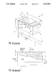
FIG. 1A-B illustrates a three-dimensional structure of the prior art of a MESFET.
FIG. 2 illustrates cross-sectional view of a MESFET according to a preferred embodiment of the present invention.
FIG. 3A-B represent steps of fabricating a MESFET according to a first preferred embodiment of the present invention.
FIG. 4 illustrates an elevated view of a superlattice grown for a MESFET according to the first preferred embodiment of the present invention.
FIG. 5 is a band diagram of a Si/Si1-x Gex heterostructure of a superlattice grown according to the first preferred embodiment of the present invention.
FIG. 6 illustrates a lateral variation of the doping density according to the present invention.
FIG. 7A-D illustrate a layer structure grown according to a second preferred embodiment of the present invention.
FIG. 2 illustrates the cross-sectional representation of a MESFET according to a preferred embodiment of the present invention. While the present invention is described in terms of a MESFET, it is contemplated that disclosed device structure and process can be applied to JFETs. The MESFET 100 has an N++ source region 102 and an N++ drain region 104. Both regions 102, 104 are formed by ion implanting N type dopant into a first semiconductor layer 110. An N type multi-region channel 106 is between the source region 102 and the drain region 104. The channel 106 has three regions: First 106A on the left side of dotted line AB and above dotted line CD; Second 106B is on the right side of dotted line AB, and above dotted line CD; and third 106C below dotted line CD. Thus, the first region 106A is of a first semiconductor material (Si) and extends from the source 102 to dotted line AB, and preferably, includes the larger part of the channel 106 under the gate 108. This region 106A is preferably, non-uniformly doped in two dimensions, with N type dopant. The second region 106B is adjacent to the first region 106A at dotted line AB and lies between 106A and the drain region 104. This second channel region 106B is, preferably, smaller than first channel region 106A, and is a superlattice of quantum wells of Si and a second semiconductor material, Si1-x Gex (where x is the Germanium mole fraction in SiGe). The third region 106C is a semi-insulating layer, which preferably may be of sapphire or, alternatively, of SiO2 or very lightly doped N-type Si (hereinafter i-type region). Each of the source region 102, gate 108, and the drain region 104, have an electrical contact 114, 116, and 118, respectively.
FIG. 3A-B show the processing steps of a first preferred embodiment of the present invention. An N-type silicon layer 120 is grown on a P silicon substrate 122 either by a Molecular Beam Epitaxy (MBE) method or by a Metal Organic Chemical Vapor Deposition (MOCVD) method. The substrate 122 has high resistivity to minimize parasitic substrate effects. N type silicon layer 120 is between 0.2 and 0.6 μm, with a doping density between 1*1016 and 5*1016 cm-3.
Next, a trench 124 is formed in the surface 126 of the N silicon layer. The surface 126 is anisotropically etched using a mixture of CF4 +O2 and RIE process. A thin thermal oxide is formed on surface 126 and selectively wet etched from the trench with BHF or, alternatively, HF, leaving the trench surfaces relatively clean and the bottom trench surface 127 is uniform (preferably planar). If the semi-insulating region 106A is other than i-type Si, the trench is etched through the silicon layer 120. The trench 124 is etched to the device's channel depth. For a short-channel MESFET with a submicron channel length (e.g., 0.1 to 0.6 μm), the desired trench depth is between 0.1 and 0.3 μm. The trench width is kept small for the construction of a short-channel MESFET. A superlattice region 128 in FIG. 3B is grown in the trench 124 to form 106B.
FIG. 4 is a representation of the superlattice structure 128 of channel region 106B, wherein five superlattice periods of Si/Si1-x Gx 130 are selectively grown in the trench 124 to result in a 1μ device. Fewer periods may be used for shorter channel devices. In the preferred embodiment, the layers are grown at an epitaxy temperature of about 600° C. on the {100}-plane of the N silicon. The layer sequence of the superlattice 128 is alternating Si1-x Gex layers, 132, 134, 136, 138, 140 each about 200 Å thick, and undoped (intrinsic) silicon layers 142, 144, 146, 148, 150 each between 300 and 1000 Å thick. First, Si1-x Gex layer 132 is grown on N silicon 120. Then, undoped silicon layer 142 is grown on Si1-x Gex layer 132. FIG. 5 is the energy band diagram of a Si/Si1-x Gex heterostructure layer 130. A 2-Dimensional Electron Gas (2-DEG) is formed in the undoped silicon side of the hetero-interface of the doped Si1-x Ge.sub. x 152 and undoped silicon 154. Each of Si1-x Gex layers 132, 134, 136, 138 and 140 has two sub layers. A first sub layer of Si0.5 Ge0.5 and a second sub layer wherein x is graded from 0.0 at the Si/SiGe interface to 0.5. Two-dimensional quantum wells are formed by the heterojunctions at each interface, 132-142, 134-144, 136-146, 138-148, and 140-150.
The Germanium mole fraction in Si1-x Gex directly influences the height of the quantum wells. In the preferred embodiment, the mole fraction of Ge is preferably 0.5 in the doped sub-layers of the Si1-x Gex and, is chosen to maximize the depth of the quantum well without causing structural dislocation of the superlattice layers. However, a smaller mole fraction, x, of Si1-x Gex may be substituted to increase the layers' defect-free thickness.
Preferred embodiment devices have improved electrical performance because they have a high doping density in the channel area 106A and a lower doping density in channel area 106B. Although it is contemplated that the doping in each superlattice layer is uniform, the source region 102 and the channel region 106A of preferred embodiment devices are non-uniformly doped with a focussed ion beam implantation technique. The implant dose is controlled such that besides varying in the y direction as in prior art devices, the doping profile is stepwise varying, with at least 1 step and preferably 5 discrete steps in the x-direction from the source 102, through channel region 106A to the edge of channel region 106B as shown in FIG. 6. Thus, in the preferred embodiment of the present invention, Ndo is no longer a constant (horizontally), but a function of x. Consequently, the doping density for the preferred embodiment device, Nd (x,y) is defined by:
N.sub.d (x,y)=N.sub.do (x)exp(-Y.sub.2)
Therefore, for the preferred embodiment device, channel doping varies in Gaussian fashion with y at each value of x. However, for a given value of y (or integrated over y), the channel doping has the form of a staircase extending from a maximum of 5-7*1018 between the source at x=0 and x=x2 to a minimum of 2-5*1017 near the edge of the superlattice, between x=x3 and x=x4. Ion implantation is followed by rapid thermal annealing and contact sintering.
Thus, with the structure of the preferred embodiment, multiple masking steps during fabrication are avoided. The dopant concentration precisely varies with position and magnitude in a single mask step. The preferred embodiment device's vertical and lateral doping profiles are simultaneously varied in a single mask step.
Once the source, channel, and the drain regions have been doped, ohmic contacts are formed by a conventional method for source, gate and drain contacts. In one embodiment, ohmic contacts are formed by thermal evaporation of 0.3 μm AuSb with the excess material lifted off of the area surrounding the contacts. To maintain a low dopant level under the gate contact, precautions must be taken to avoid altering the channel dopant density during gate contact metal deposition. Also, the gate electrode contacting the topmost layer of the Si/Si1-x Gex superlattice 150, undoped or lightly doped silicon, should not alter that layer's dopant level. This top Superlattice layer 150 in contact with the metal forms a Schottky barrier. The structure is annealed at 330° C. under protective gas for 30 seconds.
The multiple quantum wells of the preferred embodiment device create potential notches at the Si/Si1-x Gex interfaces. These potential notches, which contain 2-DEG, extend through the heterostructure region and, therefore, behave as low-resistive paths to the drain. Electrons moving through these notches have a higher mobility because scattering is minimized. This higher mobility reduces carrier transit time and delay occurring through 106B, further improving device performance.
In the preferred embodiment of the present invention the dopant level in channel region 106A is higher than the dopant level in channel regions 106B and 106C. Because the dopant density in channel region 106A is not uniform, but lower near the gate, the gate to source capacitance is reduced. However, gate to source breakdown voltage is still high enough for effective device operation. In the superlattices of region 106B, the highly doped Si1-x Gex layers 132-140 are much thinner than the undoped silicon layers 142-150 to minimize lattice mismatch structural dislocations. Consequently, superlattice quantum wells can be formed for the preferred embodiment device, the extrinsic channel resistance at the drain is significantly reduced over prior art MESFETs and JFETs and device transconductance is increased without a corresponding decrease in gain or output power.
In summary, the average channel dopant density Nd is reduced over prior art devices and junction capacitance is low. Further, the preferred embodiment device with two-dimensional graded doping has: Ndo higher (about 5-8*1018 cm-3) at the source, decreasing in a stepwise fashion to 3-5*1017 cm-3 at the superlattice edge (see FIG. 6); and, a built-in electrostatic field that accelerates electrons from the source region to the active channel region under the gate, effectively providing increased electron mobility. Thus, carrier transit time is improved with a corresponding device performance. Furthermore, the introduction of a semi-insulating or a lightly doped i-layer between the channel and the substrate significantly reduces the MESFET's gate-substrate junction capacitance. The MESFET of the preferred embodiment has an increased frequency response, both because of improved channel transit time and because of reduced device capacitance.
In a second preferred embodiment of the present invention the hetero-structure is formed by growing superlattice layers, which are sub-etched, and then, using a low temperature lateral overgrowth technique, the sub-etched areas are filled with silicon. Such a technique is disclosed in Burghartz et al., "Self-aligned bipolar epitaxial base n-p-n transistors by selective epitaxy emitter window (SEEW) technology," IEEE Trans. Electron Devices, vol. ED-38, pp. 378-385 (1991).
FIG. 7A-D illustrate the processing steps of this second preferred embodiment Si/Si1-x Gex superlattice N channel MESFET. In FIG. 7A, an N type silicon layer 202 is MBE or MOCVD grown on a semi-insulating substrate 204. The substrate 204 and the N type silicon layer 202 are identical with the substrate 122 and N type silicon layer 120 of FIG. 3A. Five superlattice 208 periods 206 of Si/Si1-x Gex are grown on N type silicon layer 202. Each superlattice period 206, has an undoped silicon layer 210, 212, 214, 216 and 218 grown on a Si1-x Gex layer 220, 222, 224, 226, and 228 respectively. The thicknesses and doping characteristics of the layers 210-218 and 220-228 are identical with those of the layers 142-150 and 132-140 respectively.
After growing the superlattice 208, the device's source-channel (S-C) and drain regions are defined. The drain region is defined when a first portion, 230 in FIG. 7B, is dry etched from the superlattice 208, using a chlorine based etchant on the Si layers to minimize thermal exposure of Si1-x Gex, and, using an SF6 and CF3 Br plasma for the Si1-x Gex layer. Next, in FIG. 7C, the etched area is filled with N silicon such that the top surface of the N silicon 240 is co-planar with the unetched top superlattice layer. The S-C region 250 is similarly defined, as represented in FIG. 7D, by etching a second superlattice portion. The structure of this second preferred embodiment, once the S-C region has been defined, is identical with the structure of the first preferred embodiment in FIG. 3B. Further processing of the second preferred embodiment MESFET is identical to that of the first.
Although the above description of the preferred embodiments of the present invention describes specific device structures, a person of ordinary skill in the art would understand that in all pertinent regions swapping P and N regions provide functionally equivalent results. Further, numerous modifications and variations will occur to a person of ordinary skill in the art without departing from the spirit and scope of the invention.
Claims (17)
1. A Field Effect Transistor (RET) with a gate, a drain, a source and further comprising:
a semi-insulating substrate; and
a multi-region channel comprising:
a first region of a first semiconductor material, said first region extending towards said drain from said source to a point under said gate beyond the midpoint of said gate,
a second region comprised of a superlattice of quantum wells, said second region extending from said first region to said drain, and,
a semi-insulating region on said semi-insulating substrate extending from said source to said drain under said first region and said second region.
2. The FET of claim 1 wherein the superlattice comprises alternating layers of said first semiconductor material and a second semiconductor material.
3. The FET of claim 1 wherein said first semiconductor material is N+ silicon.
4. The FET of claim 2 wherein said first semiconductor material is silicon and said second semiconductor material is SiGe.
5. The FET of claim 4 wherein said silicon layers are between 300 Å and 1000 Å thick and said SiGe layers are 200 Å thick.
6. The FET of claim 4 wherein the silicon layers are N+ doped to a dopant density between 1016 cm-3 and 5*1016 cm-3.
7. The FET of claim 4 wherein the mole fraction of Germanium in SiGe≦0.5.
8. The FET of claim 7 wherein the mole fraction of Germanium=0.5.
9. The FET of claim 1 wherein said multi-region channel has a laterally varying dopant density.
10. The FET of claim 1 wherein said first region has a laterally varying dopant density.
11. The FET of claim 10 wherein said laterally varying dopant density is a plurality of discrete dopant densities, whereby each of said dopant densities are in a portion of said first region.
12. The FET of claim 11 wherein said plurality of discrete dopant densities are distributed such that a maximum density is at said source, a minimum density is at the opposite end of said first region and the dopant densities uniformly decrease from said maximum to said minimum.
13. The FET of claim 1 wherein said gate is metal and said FET is a MESFET.
14. The FET of claim 1 wherein said gate is doped semiconductor and said FET is a JFET.
15. The FET of claim 1 wherein said semi-insulating region is a region of i-type silicon.
16. The FET of claim 1 wherein said semi-insulating region is an insulating region of sapphire.
17. The FET of claim 1 wherein said semi-insulating region is an insulating region of SiO2.
Priority Applications (4)
| Application Number | Priority Date | Filing Date | Title |
|---|---|---|---|
| US07/995,459 US5323020A (en) | 1992-12-22 | 1992-12-22 | High performance MESFET with multiple quantum wells |
| JP5260052A JP2504376B2 (en) | 1992-12-22 | 1993-10-18 | Field effect transistor |
| EP93480207A EP0607729A3 (en) | 1992-12-22 | 1993-12-03 | High performance MESFET with multiple quantum wells. |
| US08/198,938 US5420059A (en) | 1992-12-22 | 1994-02-18 | Method of making a high performance MESFET with multiple quantum wells |
Applications Claiming Priority (1)
| Application Number | Priority Date | Filing Date | Title |
|---|---|---|---|
| US07/995,459 US5323020A (en) | 1992-12-22 | 1992-12-22 | High performance MESFET with multiple quantum wells |
Related Child Applications (1)
| Application Number | Title | Priority Date | Filing Date |
|---|---|---|---|
| US08/198,938 Division US5420059A (en) | 1992-12-22 | 1994-02-18 | Method of making a high performance MESFET with multiple quantum wells |
Publications (1)
| Publication Number | Publication Date |
|---|---|
| US5323020A true US5323020A (en) | 1994-06-21 |
Family
ID=25541833
Family Applications (2)
| Application Number | Title | Priority Date | Filing Date |
|---|---|---|---|
| US07/995,459 Expired - Lifetime US5323020A (en) | 1992-12-22 | 1992-12-22 | High performance MESFET with multiple quantum wells |
| US08/198,938 Expired - Lifetime US5420059A (en) | 1992-12-22 | 1994-02-18 | Method of making a high performance MESFET with multiple quantum wells |
Family Applications After (1)
| Application Number | Title | Priority Date | Filing Date |
|---|---|---|---|
| US08/198,938 Expired - Lifetime US5420059A (en) | 1992-12-22 | 1994-02-18 | Method of making a high performance MESFET with multiple quantum wells |
Country Status (3)
| Country | Link |
|---|---|
| US (2) | US5323020A (en) |
| EP (1) | EP0607729A3 (en) |
| JP (1) | JP2504376B2 (en) |
Cited By (16)
| Publication number | Priority date | Publication date | Assignee | Title |
|---|---|---|---|---|
| US5500391A (en) * | 1994-08-09 | 1996-03-19 | At&T Corp. | Method for making a semiconductor device including diffusion control |
| US5665981A (en) * | 1994-10-24 | 1997-09-09 | Micron Technology, Inc. | Thin film transistors and method of promoting large crystal grain size in the formation of polycrystalline silicon alloy thin films |
| FR2766619A1 (en) * | 1997-04-25 | 1999-01-29 | Daimler Benz Ag | HIGH MODULATION EFFICIENCY HETEROSTRUCTURE FIELD-EFFECT TRANSISTORS |
| US6229177B1 (en) * | 1998-03-30 | 2001-05-08 | Advanced Micro Devices, Inc. | Semiconductor with laterally non-uniform channel doping profile |
| US6355963B1 (en) * | 1994-11-16 | 2002-03-12 | Matsushita Electric Industrial Co., Ltd. | MOS type semiconductor device having an impurity diffusion layer |
| US20060138581A1 (en) * | 2004-12-23 | 2006-06-29 | Micron Technology, Inc. | Split transfer gate for dark current suppression in an imager pixel |
| US7224007B1 (en) * | 2004-01-12 | 2007-05-29 | Advanced Micro Devices, Inc. | Multi-channel transistor with tunable hot carrier effect |
| US20100052015A1 (en) * | 2008-08-26 | 2010-03-04 | Sanken Electric Co., Ltd. | Semiconductor device |
| US20100123203A1 (en) * | 2008-11-18 | 2010-05-20 | Krishna Kumar Bhuwalka | Tunnel Field-Effect Transistor with Metal Source |
| US20100276732A1 (en) * | 2007-12-26 | 2010-11-04 | Yuji Ando | Semiconductor device |
| US20110027959A1 (en) * | 2008-09-05 | 2011-02-03 | Taiwan Semiconductor Manufacturing Company, Ltd. | Tunnel Field-Effect Transistors with Superlattice Channels |
| US8697510B2 (en) | 2007-07-25 | 2014-04-15 | Taiwan Semiconductor Manufacturing Company, Ltd. | Tunnel field-effect transistor with narrow band-gap channel and strong gate coupling |
| WO2015114482A1 (en) * | 2014-01-29 | 2015-08-06 | International Business Machines Corporation | Semiconductor device including superlattice sige/si fin structure |
| US9790085B1 (en) * | 2016-06-16 | 2017-10-17 | Nxp Usa, Inc. | Actively preventing charge induced leakage of semiconductor devices |
| US10797137B2 (en) * | 2017-06-30 | 2020-10-06 | Taiwan Semiconductor Manufacturing Co., Ltd. | Method for reducing Schottky barrier height and semiconductor device with reduced Schottky barrier height |
| US11121254B2 (en) * | 2019-08-19 | 2021-09-14 | United Microelectronics Corp. | Transistor with strained superlattice as source/drain region |
Families Citing this family (5)
| Publication number | Priority date | Publication date | Assignee | Title |
|---|---|---|---|---|
| US5753545A (en) * | 1994-12-01 | 1998-05-19 | Hughes Electronics Corporation | Effective constant doping in a graded compositional alloy |
| US6873362B1 (en) * | 1995-03-22 | 2005-03-29 | Sony Corporation | Scanning switch transistor for solid-state imaging device |
| US6399970B2 (en) | 1996-09-17 | 2002-06-04 | Matsushita Electric Industrial Co., Ltd. | FET having a Si/SiGeC heterojunction channel |
| KR100451039B1 (en) * | 2000-12-20 | 2004-10-02 | 주식회사 하이닉스반도체 | Method of forming a gate electrode in a semiconductor device |
| JP2005319895A (en) | 2004-05-10 | 2005-11-17 | Kawasaki Heavy Ind Ltd | Stand riding type small planing boat |
Citations (3)
| Publication number | Priority date | Publication date | Assignee | Title |
|---|---|---|---|---|
| US4163237A (en) * | 1978-04-24 | 1979-07-31 | Bell Telephone Laboratories, Incorporated | High mobility multilayered heterojunction devices employing modulated doping |
| US4673959A (en) * | 1983-12-28 | 1987-06-16 | Hitachi, Ltd. | Heterojunction FET with doubly-doped channel |
| US4879256A (en) * | 1985-06-05 | 1989-11-07 | At&T Bell Laboratories | Method of controlling the order-disorder state in a semiconductor device |
Family Cites Families (22)
| Publication number | Priority date | Publication date | Assignee | Title |
|---|---|---|---|---|
| US4261771A (en) * | 1979-10-31 | 1981-04-14 | Bell Telephone Laboratories, Incorporated | Method of fabricating periodic monolayer semiconductor structures by molecular beam epitaxy |
| JPS59181069A (en) * | 1983-03-30 | 1984-10-15 | Fujitsu Ltd | Semiconductor device |
| DE3480631D1 (en) * | 1983-06-24 | 1990-01-04 | Nec Corp | SEMICONDUCTOR STRUCTURE WITH HIGH GRID DENSITY. |
| JPS6052062A (en) * | 1983-08-31 | 1985-03-23 | Nec Corp | Field-effect transistor |
| JPS6317562A (en) * | 1986-07-10 | 1988-01-25 | Toshiba Corp | Superlattice element and its manufacture |
| US4908678A (en) * | 1986-10-08 | 1990-03-13 | Semiconductor Energy Laboratory Co., Ltd. | FET with a super lattice channel |
| US4999682A (en) * | 1987-08-14 | 1991-03-12 | Regents Of The University Of Minnesota | Electronic and optoelectronic laser devices utilizing light hole properties |
| JPS6481274A (en) * | 1987-09-22 | 1989-03-27 | Matsushita Electric Ind Co Ltd | Semiconductor device |
| US4863877A (en) * | 1987-11-13 | 1989-09-05 | Kopin Corporation | Ion implantation and annealing of compound semiconductor layers |
| US4839310A (en) * | 1988-01-27 | 1989-06-13 | Massachusetts Institute Of Technology | High mobility transistor with opposed-gates |
| JPH01243591A (en) * | 1988-03-25 | 1989-09-28 | Hitachi Ltd | Semiconductor device |
| US5104823A (en) * | 1988-03-31 | 1992-04-14 | Northern Telecom Limited | Monolithic integration of optoelectronic and electronic devices |
| JPH02205325A (en) * | 1989-02-03 | 1990-08-15 | Sharp Corp | Semiconductor device |
| DE69030129T2 (en) * | 1989-04-12 | 1997-10-09 | Sumitomo Electric Industries | Manufacturing process of a semiconductor integrated circuit |
| JP3194941B2 (en) * | 1990-03-19 | 2001-08-06 | 富士通株式会社 | Semiconductor device |
| JP2855775B2 (en) * | 1990-04-20 | 1999-02-10 | 日本電気株式会社 | Field effect transistor |
| US5266506A (en) * | 1990-07-31 | 1993-11-30 | At&T Bell Laboratories | Method of making substantially linear field-effect transistor |
| US5155571A (en) * | 1990-08-06 | 1992-10-13 | The Regents Of The University Of California | Complementary field effect transistors having strained superlattice structure |
| US5081511A (en) * | 1990-09-06 | 1992-01-14 | Motorola, Inc. | Heterojunction field effect transistor with monolayers in channel region |
| US5104824A (en) * | 1990-11-06 | 1992-04-14 | Bell Communications Research, Inc. | Selective area regrowth for surface-emitting lasers and other sharp features |
| US5142349A (en) * | 1991-07-01 | 1992-08-25 | Motorola, Inc. | Self-doped high performance complementary heterojunction field effect transistor |
| US5219772A (en) * | 1991-08-15 | 1993-06-15 | At&T Bell Laboratories | Method for making field effect devices with ultra-short gates |
-
1992
- 1992-12-22 US US07/995,459 patent/US5323020A/en not_active Expired - Lifetime
-
1993
- 1993-10-18 JP JP5260052A patent/JP2504376B2/en not_active Expired - Lifetime
- 1993-12-03 EP EP93480207A patent/EP0607729A3/en not_active Withdrawn
-
1994
- 1994-02-18 US US08/198,938 patent/US5420059A/en not_active Expired - Lifetime
Patent Citations (3)
| Publication number | Priority date | Publication date | Assignee | Title |
|---|---|---|---|---|
| US4163237A (en) * | 1978-04-24 | 1979-07-31 | Bell Telephone Laboratories, Incorporated | High mobility multilayered heterojunction devices employing modulated doping |
| US4673959A (en) * | 1983-12-28 | 1987-06-16 | Hitachi, Ltd. | Heterojunction FET with doubly-doped channel |
| US4879256A (en) * | 1985-06-05 | 1989-11-07 | At&T Bell Laboratories | Method of controlling the order-disorder state in a semiconductor device |
Non-Patent Citations (6)
| Title |
|---|
| A. F. Evason, et al., "Fabrication and Performance of GaAs MESFET's With Graded Channel Doping Using Focused Ion-Beam Implantation" IEEE Electron Device Letters, vol. 9, No. 6, pp. 281-283, Jun. 1988. |
| A. F. Evason, et al., Fabrication and Performance of GaAs MESFET s With Graded Channel Doping Using Focused Ion Beam Implantation IEEE Electron Device Letters, vol. 9, No. 6, pp. 281 283, Jun. 1988. * |
| P. C. Chao, et al., "Channel-Length Effects in Quarter-Micrometer Gate-Length GaAs MESFET's" IEEE Electron Device Letters, vol. EDL-4, No. 9, pp. 326-328, Sep. 1983. |
| P. C. Chao, et al., "Experimental Comparisons in the Electrical Performance of Long and Ultrashort Gate Length GaAs MESFET's" IEEE Electron Device Letters, vol. EDL-3, No. 8, pp. 187-283, Aug. 1982. |
| P. C. Chao, et al., Channel Length Effects in Quarter Micrometer Gate Length GaAs MESFET s IEEE Electron Device Letters, vol. EDL 4, No. 9, pp. 326 328, Sep. 1983. * |
| P. C. Chao, et al., Experimental Comparisons in the Electrical Performance of Long and Ultrashort Gate Length GaAs MESFET s IEEE Electron Device Letters, vol. EDL 3, No. 8, pp. 187 283, Aug. 1982. * |
Cited By (29)
| Publication number | Priority date | Publication date | Assignee | Title |
|---|---|---|---|---|
| US5500391A (en) * | 1994-08-09 | 1996-03-19 | At&T Corp. | Method for making a semiconductor device including diffusion control |
| US5665981A (en) * | 1994-10-24 | 1997-09-09 | Micron Technology, Inc. | Thin film transistors and method of promoting large crystal grain size in the formation of polycrystalline silicon alloy thin films |
| US5977560A (en) * | 1994-10-24 | 1999-11-02 | Micron Technology, Inc. | Thin film transistor constructions with polycrystalline silicon-germanium alloy doped with carbon in the channel region |
| US5985703A (en) * | 1994-10-24 | 1999-11-16 | Banerjee; Sanjay | Method of making thin film transistors |
| US6320202B1 (en) | 1994-10-24 | 2001-11-20 | Micron Technology, Inc. | Bottom-gated thin film transistors comprising germanium in a channel region |
| US6355963B1 (en) * | 1994-11-16 | 2002-03-12 | Matsushita Electric Industrial Co., Ltd. | MOS type semiconductor device having an impurity diffusion layer |
| FR2766619A1 (en) * | 1997-04-25 | 1999-01-29 | Daimler Benz Ag | HIGH MODULATION EFFICIENCY HETEROSTRUCTURE FIELD-EFFECT TRANSISTORS |
| US6229177B1 (en) * | 1998-03-30 | 2001-05-08 | Advanced Micro Devices, Inc. | Semiconductor with laterally non-uniform channel doping profile |
| US7224007B1 (en) * | 2004-01-12 | 2007-05-29 | Advanced Micro Devices, Inc. | Multi-channel transistor with tunable hot carrier effect |
| US7696597B2 (en) | 2004-12-23 | 2010-04-13 | Aptina Imaging Corporation | Split transfer gate for dark current suppression in an imager pixel |
| US20060138581A1 (en) * | 2004-12-23 | 2006-06-29 | Micron Technology, Inc. | Split transfer gate for dark current suppression in an imager pixel |
| US7642107B2 (en) | 2004-12-23 | 2010-01-05 | Aptina Imaging Corporation | Split transfer gate for dark current suppression an imager pixel |
| US7663167B2 (en) * | 2004-12-23 | 2010-02-16 | Aptina Imaging Corp. | Split transfer gate for dark current suppression in an imager pixel |
| US20070102781A1 (en) * | 2004-12-23 | 2007-05-10 | John Ladd | Split transfer gate for dark current suppression an imager pixel |
| US8697510B2 (en) | 2007-07-25 | 2014-04-15 | Taiwan Semiconductor Manufacturing Company, Ltd. | Tunnel field-effect transistor with narrow band-gap channel and strong gate coupling |
| US8344422B2 (en) * | 2007-12-26 | 2013-01-01 | Nec Corporation | Semiconductor device |
| US20100276732A1 (en) * | 2007-12-26 | 2010-11-04 | Yuji Ando | Semiconductor device |
| US20100052015A1 (en) * | 2008-08-26 | 2010-03-04 | Sanken Electric Co., Ltd. | Semiconductor device |
| US8159004B2 (en) * | 2008-08-26 | 2012-04-17 | Sanken Electric Co., Ltd. | Compound semiconductor device having dopant concentration gradient |
| US8669163B2 (en) | 2008-09-05 | 2014-03-11 | Taiwan Semiconductor Manufacturing Company, Ltd. | Tunnel field-effect transistors with superlattice channels |
| US20110027959A1 (en) * | 2008-09-05 | 2011-02-03 | Taiwan Semiconductor Manufacturing Company, Ltd. | Tunnel Field-Effect Transistors with Superlattice Channels |
| US8587075B2 (en) | 2008-11-18 | 2013-11-19 | Taiwan Semiconductor Manufacturing Company, Ltd. | Tunnel field-effect transistor with metal source |
| US20100123203A1 (en) * | 2008-11-18 | 2010-05-20 | Krishna Kumar Bhuwalka | Tunnel Field-Effect Transistor with Metal Source |
| WO2015114482A1 (en) * | 2014-01-29 | 2015-08-06 | International Business Machines Corporation | Semiconductor device including superlattice sige/si fin structure |
| US9790085B1 (en) * | 2016-06-16 | 2017-10-17 | Nxp Usa, Inc. | Actively preventing charge induced leakage of semiconductor devices |
| US10797137B2 (en) * | 2017-06-30 | 2020-10-06 | Taiwan Semiconductor Manufacturing Co., Ltd. | Method for reducing Schottky barrier height and semiconductor device with reduced Schottky barrier height |
| US11502174B2 (en) | 2017-06-30 | 2022-11-15 | Taiwan Semiconductor Manufacturing Co., Ltd. | Method for reducing Schottky barrier height and semiconductor device with reduced Schottky barrier height |
| US11817481B2 (en) | 2017-06-30 | 2023-11-14 | Taiwan Semiconductor Manufacturing Company, Ltd. | Method for reducing Schottky barrier height and semiconductor device with reduced Schottky barrier height |
| US11121254B2 (en) * | 2019-08-19 | 2021-09-14 | United Microelectronics Corp. | Transistor with strained superlattice as source/drain region |
Also Published As
| Publication number | Publication date |
|---|---|
| EP0607729A2 (en) | 1994-07-27 |
| EP0607729A3 (en) | 1995-02-22 |
| JPH07211891A (en) | 1995-08-11 |
| JP2504376B2 (en) | 1996-06-05 |
| US5420059A (en) | 1995-05-30 |
Similar Documents
| Publication | Publication Date | Title |
|---|---|---|
| US5323020A (en) | High performance MESFET with multiple quantum wells | |
| US4641161A (en) | Heterojunction device | |
| US4471366A (en) | Field effect transistor with high cut-off frequency and process for forming same | |
| US4916498A (en) | High electron mobility power transistor | |
| WO1989007333A1 (en) | Vertical transistor device fabricated with semiconductor regrowth | |
| US4908325A (en) | Method of making heterojunction transistors with wide band-gap stop etch layer | |
| US5488237A (en) | Semiconductor device with delta-doped layer in channel region | |
| WO1988003328A1 (en) | Striped-channel transistor and method of forming the same | |
| EP0566591B1 (en) | Semiconductor device | |
| EP0201873A2 (en) | A method of the production of a metal semiconductor field effect transistor and said transistor | |
| JP3262056B2 (en) | Bipolar transistor and manufacturing method thereof | |
| US5276340A (en) | Semiconductor integrated circuit having a reduced side gate effect | |
| EP0613189A2 (en) | Channel structure for field effect transistor and method of manufacturing the same | |
| US6278144B1 (en) | Field-effect transistor and method for manufacturing the field effect transistor | |
| US5552330A (en) | Resonant tunneling fet and methods of fabrication | |
| US5877047A (en) | Lateral gate, vertical drift region transistor | |
| US5381027A (en) | Semiconductor device having a heterojunction and a two dimensional gas as an active layer | |
| US4994868A (en) | Heterojunction confined channel FET | |
| US4962050A (en) | GaAs FET manufacturing process employing channel confining layers | |
| US5258631A (en) | Semiconductor device having a two-dimensional electron gas as an active layer | |
| KR100563884B1 (en) | Manufacturing method of a junction field effect transistor | |
| EP0469768A1 (en) | A substantially linear field effect transistor and method of making same | |
| JP2643890B2 (en) | Tunnel transistor | |
| JP3653652B2 (en) | Semiconductor device | |
| GB2239557A (en) | High electron mobility transistors |
Legal Events
| Date | Code | Title | Description |
|---|---|---|---|
| AS | Assignment |
Owner name: INTERNATIONAL BUSINESS MACHINES CORPORATION, NEW Y Free format text: ASSIGNMENT OF ASSIGNORS INTEREST;ASSIGNORS:MOHAMMAD, S. NOOR;RENBECK, ROBERT B.;REEL/FRAME:006600/0081 Effective date: 19921221 |
|
| STCF | Information on status: patent grant |
Free format text: PATENTED CASE |
|
| CC | Certificate of correction | ||
| FPAY | Fee payment |
Year of fee payment: 4 |
|
| FPAY | Fee payment |
Year of fee payment: 8 |
|
| FPAY | Fee payment |
Year of fee payment: 12 |