US5332469A - Capacitive surface micromachined differential pressure sensor - Google Patents
Capacitive surface micromachined differential pressure sensor Download PDFInfo
- Publication number
- US5332469A US5332469A US08/014,025 US1402593A US5332469A US 5332469 A US5332469 A US 5332469A US 1402593 A US1402593 A US 1402593A US 5332469 A US5332469 A US 5332469A
- Authority
- US
- United States
- Prior art keywords
- layer
- diaphragm
- substrate
- depositing
- sacrificial
- Prior art date
- Legal status (The legal status is an assumption and is not a legal conclusion. Google has not performed a legal analysis and makes no representation as to the accuracy of the status listed.)
- Expired - Fee Related
Links
Images


Classifications
-
- B—PERFORMING OPERATIONS; TRANSPORTING
- B81—MICROSTRUCTURAL TECHNOLOGY
- B81C—PROCESSES OR APPARATUS SPECIALLY ADAPTED FOR THE MANUFACTURE OR TREATMENT OF MICROSTRUCTURAL DEVICES OR SYSTEMS
- B81C1/00—Manufacture or treatment of devices or systems in or on a substrate
- B81C1/00436—Shaping materials, i.e. techniques for structuring the substrate or the layers on the substrate
- B81C1/00444—Surface micromachining, i.e. structuring layers on the substrate
- B81C1/00468—Releasing structures
- B81C1/00476—Releasing structures removing a sacrificial layer
-
- B—PERFORMING OPERATIONS; TRANSPORTING
- B23—MACHINE TOOLS; METAL-WORKING NOT OTHERWISE PROVIDED FOR
- B23P—METAL-WORKING NOT OTHERWISE PROVIDED FOR; COMBINED OPERATIONS; UNIVERSAL MACHINE TOOLS
- B23P15/00—Making specific metal objects by operations not covered by a single other subclass or a group in this subclass
-
- B—PERFORMING OPERATIONS; TRANSPORTING
- B81—MICROSTRUCTURAL TECHNOLOGY
- B81B—MICROSTRUCTURAL DEVICES OR SYSTEMS, e.g. MICROMECHANICAL DEVICES
- B81B3/00—Devices comprising flexible or deformable elements, e.g. comprising elastic tongues or membranes
- B81B3/0002—Arrangements for avoiding sticking of the flexible or moving parts
- B81B3/0013—Structures dimensioned for mechanical prevention of stiction, e.g. spring with increased stiffness
-
- B—PERFORMING OPERATIONS; TRANSPORTING
- B81—MICROSTRUCTURAL TECHNOLOGY
- B81C—PROCESSES OR APPARATUS SPECIALLY ADAPTED FOR THE MANUFACTURE OR TREATMENT OF MICROSTRUCTURAL DEVICES OR SYSTEMS
- B81C1/00—Manufacture or treatment of devices or systems in or on a substrate
- B81C1/00912—Treatments or methods for avoiding stiction of flexible or moving parts of MEMS
- B81C1/0092—For avoiding stiction during the manufacturing process of the device, e.g. during wet etching
- B81C1/00944—Maintaining a critical distance between the structures to be released
-
- G—PHYSICS
- G01—MEASURING; TESTING
- G01L—MEASURING FORCE, STRESS, TORQUE, WORK, MECHANICAL POWER, MECHANICAL EFFICIENCY, OR FLUID PRESSURE
- G01L9/00—Measuring steady of quasi-steady pressure of fluid or fluent solid material by electric or magnetic pressure-sensitive elements; Transmitting or indicating the displacement of mechanical pressure-sensitive elements, used to measure the steady or quasi-steady pressure of a fluid or fluent solid material, by electric or magnetic means
- G01L9/0041—Transmitting or indicating the displacement of flexible diaphragms
- G01L9/0042—Constructional details associated with semiconductive diaphragm sensors, e.g. etching, or constructional details of non-semiconductive diaphragms
-
- G—PHYSICS
- G01—MEASURING; TESTING
- G01L—MEASURING FORCE, STRESS, TORQUE, WORK, MECHANICAL POWER, MECHANICAL EFFICIENCY, OR FLUID PRESSURE
- G01L9/00—Measuring steady of quasi-steady pressure of fluid or fluent solid material by electric or magnetic pressure-sensitive elements; Transmitting or indicating the displacement of mechanical pressure-sensitive elements, used to measure the steady or quasi-steady pressure of a fluid or fluent solid material, by electric or magnetic means
- G01L9/0041—Transmitting or indicating the displacement of flexible diaphragms
- G01L9/0072—Transmitting or indicating the displacement of flexible diaphragms using variations in capacitance
- G01L9/0073—Transmitting or indicating the displacement of flexible diaphragms using variations in capacitance using a semiconductive diaphragm
-
- G—PHYSICS
- G01—MEASURING; TESTING
- G01P—MEASURING LINEAR OR ANGULAR SPEED, ACCELERATION, DECELERATION, OR SHOCK; INDICATING PRESENCE, ABSENCE, OR DIRECTION, OF MOVEMENT
- G01P15/00—Measuring acceleration; Measuring deceleration; Measuring shock, i.e. sudden change of acceleration
- G01P15/02—Measuring acceleration; Measuring deceleration; Measuring shock, i.e. sudden change of acceleration by making use of inertia forces using solid seismic masses
- G01P15/08—Measuring acceleration; Measuring deceleration; Measuring shock, i.e. sudden change of acceleration by making use of inertia forces using solid seismic masses with conversion into electric or magnetic values
- G01P15/0802—Details
-
- H—ELECTRICITY
- H01—ELECTRIC ELEMENTS
- H01L—SEMICONDUCTOR DEVICES NOT COVERED BY CLASS H10
- H01L21/00—Processes or apparatus adapted for the manufacture or treatment of semiconductor or solid state devices or of parts thereof
- H01L21/67—Apparatus specially adapted for handling semiconductor or electric solid state devices during manufacture or treatment thereof; Apparatus specially adapted for handling wafers during manufacture or treatment of semiconductor or electric solid state devices or components ; Apparatus not specifically provided for elsewhere
- H01L21/683—Apparatus specially adapted for handling semiconductor or electric solid state devices during manufacture or treatment thereof; Apparatus specially adapted for handling wafers during manufacture or treatment of semiconductor or electric solid state devices or components ; Apparatus not specifically provided for elsewhere for supporting or gripping
- H01L21/6835—Apparatus specially adapted for handling semiconductor or electric solid state devices during manufacture or treatment thereof; Apparatus specially adapted for handling wafers during manufacture or treatment of semiconductor or electric solid state devices or components ; Apparatus not specifically provided for elsewhere for supporting or gripping using temporarily an auxiliary support
-
- B—PERFORMING OPERATIONS; TRANSPORTING
- B81—MICROSTRUCTURAL TECHNOLOGY
- B81B—MICROSTRUCTURAL DEVICES OR SYSTEMS, e.g. MICROMECHANICAL DEVICES
- B81B2201/00—Specific applications of microelectromechanical systems
- B81B2201/02—Sensors
- B81B2201/0264—Pressure sensors
-
- B—PERFORMING OPERATIONS; TRANSPORTING
- B81—MICROSTRUCTURAL TECHNOLOGY
- B81C—PROCESSES OR APPARATUS SPECIALLY ADAPTED FOR THE MANUFACTURE OR TREATMENT OF MICROSTRUCTURAL DEVICES OR SYSTEMS
- B81C2201/00—Manufacture or treatment of microstructural devices or systems
- B81C2201/01—Manufacture or treatment of microstructural devices or systems in or on a substrate
- B81C2201/0101—Shaping material; Structuring the bulk substrate or layers on the substrate; Film patterning
- B81C2201/0128—Processes for removing material
- B81C2201/013—Etching
- B81C2201/0135—Controlling etch progression
- B81C2201/014—Controlling etch progression by depositing an etch stop layer, e.g. silicon nitride, silicon oxide, metal
-
- H—ELECTRICITY
- H01—ELECTRIC ELEMENTS
- H01L—SEMICONDUCTOR DEVICES NOT COVERED BY CLASS H10
- H01L2924/00—Indexing scheme for arrangements or methods for connecting or disconnecting semiconductor or solid-state bodies as covered by H01L24/00
- H01L2924/19—Details of hybrid assemblies other than the semiconductor or other solid state devices to be connected
- H01L2924/1901—Structure
- H01L2924/1904—Component type
- H01L2924/19041—Component type being a capacitor
-
- H—ELECTRICITY
- H01—ELECTRIC ELEMENTS
- H01L—SEMICONDUCTOR DEVICES NOT COVERED BY CLASS H10
- H01L2924/00—Indexing scheme for arrangements or methods for connecting or disconnecting semiconductor or solid-state bodies as covered by H01L24/00
- H01L2924/30—Technical effects
- H01L2924/301—Electrical effects
- H01L2924/30105—Capacitance
-
- Y—GENERAL TAGGING OF NEW TECHNOLOGICAL DEVELOPMENTS; GENERAL TAGGING OF CROSS-SECTIONAL TECHNOLOGIES SPANNING OVER SEVERAL SECTIONS OF THE IPC; TECHNICAL SUBJECTS COVERED BY FORMER USPC CROSS-REFERENCE ART COLLECTIONS [XRACs] AND DIGESTS
- Y10—TECHNICAL SUBJECTS COVERED BY FORMER USPC
- Y10S—TECHNICAL SUBJECTS COVERED BY FORMER USPC CROSS-REFERENCE ART COLLECTIONS [XRACs] AND DIGESTS
- Y10S438/00—Semiconductor device manufacturing: process
- Y10S438/977—Thinning or removal of substrate
-
- Y—GENERAL TAGGING OF NEW TECHNOLOGICAL DEVELOPMENTS; GENERAL TAGGING OF CROSS-SECTIONAL TECHNOLOGIES SPANNING OVER SEVERAL SECTIONS OF THE IPC; TECHNICAL SUBJECTS COVERED BY FORMER USPC CROSS-REFERENCE ART COLLECTIONS [XRACs] AND DIGESTS
- Y10—TECHNICAL SUBJECTS COVERED BY FORMER USPC
- Y10T—TECHNICAL SUBJECTS COVERED BY FORMER US CLASSIFICATION
- Y10T29/00—Metal working
- Y10T29/49—Method of mechanical manufacture
- Y10T29/49002—Electrical device making
- Y10T29/49082—Resistor making
- Y10T29/49103—Strain gauge making
Definitions
- a sacrificial layer In order to build microstructures, a sacrificial layer first must be deposited on a substrate, and then a structural component or layer is deposited on the sacrificial layer. The sacrificial layer is then removed, leaving a substrate with a structural component attached to, but spaced from, the substrate.
- Two types of processes are currently used to remove the sacrificial layer. One type is the wet-release method, and the other type is the dry-release method.
- etching solution or etchant is applied between the substrate and the structural layer to remove the sacrificial layer. Then, the sacrificial layer is rinsed away by a rinsing solution. As the etching and rinsing solutions evaporate from the small space between the structural layer and the substrate, strong capillary forces between the two are created. As the volume of liquid trapped beneath the structural layer decreases by evaporation, the capillary forces become stronger. As a result of these forces, the structural layer begins to deflect toward the surface of the substrate. If the capillary forces are strong enough, and the structural layer weak enough, the structural layer deforms to the point where it contacts the substrate. At that point, intersolid forces are the strongest, and the structural layer may be permanently pinned to the substrate. Therefore, a need exists for a method that prevents the destructive effects of the capillary forces associated with wet etching techniques.
- dry-release methods have been developed. While the dry-release methods for removing sacrificial layers are not troubled by capillary forces, they have their own distinct drawbacks.
- the dry-release method of Saiki in U.S. Pat. No. 3,846,166 requires deposition of a structural layer on a sacrificial resin layer.
- the resin layer melts or degrades at low temperatures (e.g., 300°-400° C.) many desirable materials for the structural layer which require higher deposition temperatures cannot be deposited upon the fragile sacrificial resin layer.
- polysilicon a preferred material for microstructures, requires a temperature of about 600° C. for deposition.
- the dry-release method of the present invention produces temporary posts or columns that support the structural layer during the wet etching of the sacrificial layer.
- the posts or columns Preferably made of a polymer, the posts or columns prevent the structural layer from being pulled toward the substrate by capillary forces as the etching and rinsing solutions evaporate.
- the temporary posts or columns extend from the substrate to the structural layer during the wet etching staging, and, after removal of the sacrificial layer, are themselves removed by dry etching with plasma to produce a microstructure that contains no posts or columns. This step of dry etching the plasma requires no liquids. Therefore, capillary forces are not present, and additional supports are not needed during this step.
- the method for fabricating the micromachined differential pressure sensor on a semiconductor substrate includes the steps of selectively implanting a doping material into the substrate to define a first etch-stop layer.
- a surface layer of semiconductor material is then deposited Over the substrate so as to cover the first etch-stop layer and thereby define a diaphragm area.
- a passivating conductive layer is deposited over the diaphragm area to form a diaphragm electrode.
- a sacrificial layer is selectively deposited on the diaphragm area, A conductive structural layer is anchored to the surface layer such that the sacrificial layer is located between the substrate and the structural layer so as to form a second electrode.
- the substrate is selectively etched from the side opposite the structural layer so as to form a backside aperture that terminates at the first etch-stop layer,
- the first etch-stop layer is then removed such that the backside aperture couples to the diaphragm layer.
- the sacrificial layer is removed and then the temporary posts are removed.
- the resulting differential pressure sensor produces a variation in the output capacitance when a pressure is exerted through the backside aperture causing a deflection of the diaphragm and a corresponding change in the capacitance between the first and second electrodes.
- a reference capacitor constructed without a diaphragm is also provided on the substrate adjacent to the pressure sensor.
- FIG. 1 is a frontal sectioned view through the substrate along section lines 1--1 of FIG. 2 showing the pressure and the reference sensor elements.
- FIG. 2 is a top view of the differential pressure sensor.
- FIG. 3 is a chart showing the design optimization variables for the differential pressure sensor.
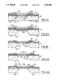
- FIGS. 4A-4O illustrate frontal section views of the pressure sensor in accordance with the present invention.
- FIG. 5 illustrates the sensor transfer function
- the present invention relates to a capacitive surface micromachined sensor suitable for the measurement of liquid and gas pressures that can be manufactured without the use of wafer bonding techniques.
- the present pressure sensor is optimized for the measurement of differential pressure of liquids such as engine, suspension, and transmission oil.
- this design consists of a two-plate air dielectric capacitor. One plate is a diaphragm which is mechanically deformed by the pressure narrowing the gap and changing its capacitance. The pressure of the liquid is applied to the backside of the diaphragm through a pressure port.
- a matching capacitor is constructed adjacent to the transducer for the ratiometric measurement of the diaphragm deflection.
- This design uses a single crystal silicon diaphragm for the moving electrode and polycrystalline silicon for the stationary electrode.
- This design exploits the high quality and reproducibility of the mechanical properties of single crystal silicon for the analog diaphragm, and the versatility of polysilicon micromachining for the fabrication of suspended parts.
- the gap separation distance is less than a micrometer, which yields a device capacitance of a few picofarads. This capacitance is large enough to be sensed with off chip circuits.
- the four bonding pads a, b, c and d for the electrodes are located on the same side of the chip for easy interconnection to the detection circuit. These devices can be manufactured to meet a ⁇ 10% error specification in their capacitance to pressure characteristic without calibration. This manufacturing accuracy and reproducibility reduces the sensor cost significantly.
- the design for this device is illustrated in an engine oil pressure sensor application.
- the sensor must satisfy several design criteria: a) the capacitance of the sensor must be above a specified minimum C min ; b) the device must have a full pressure range of P r , and it must be able to withstand the overpressure P ov ; c) the pull-in voltage of the top polysilicon plate must be greater than V pmin ; and d) the variability of the load deflection curve subject to process variations must be below a threshold ⁇ O . Furthermore, the area and cost must be minimized in order to minimize manufacturing costs.
- the pull-in voltage of the capacitor is the voltage at which the electrical force between the plates is strong enough to make the capacitor collapse.
- the upper electrode is more compliant than the diaphragm, hence it determines this voltage. It can be shown that the pull-in voltage for a clamped elastic plate of thickness s is ##EQU5##
- Equation (2) eliminates one of the design variables, leaving only three.
- Equation (5) indicates that the stationary electrode should be made as thick as possible to maximize the pull-in voltage.
- Equation (3) limits the feasible region to the points in the quadrant below the straight line A.
- the capacitance constraint of Equation (4) combined with Equation (2) yields the curve ##EQU8## represented by the curve B.
- the pull-in voltage of Equations (5) and (2) yield the curve C ##EQU9##
- the shadowed area is the feasible design region, and the point P minimizes the total width (and cost) of the device while meeting all the constraints. Note that not all the constraints may be active since for some particular design parameters the constraints may land outside the boundaries of the feasible region.
- the diaphragm is 530 ⁇ m wide, and 19 ⁇ m thick, with a gap of 0.7 ⁇ m.
- the resulting capacitance is approximately 3.5 pF per device with a 0.8 pF full scale span and can measure pressures of up to 100 PSI.
- FIG. 4 illustrates the fabrication sequence of the preferred embodiment of the present invention
- the process starts at FIG. 4A with a p-type silicon wafer 10 having a 100 crystal lattice orientation and with a boron concentration of 10 15 cm -3
- the silicon first is etched about 1 ⁇ m deep using an SF 6 plasma.
- the wafer is patterned again to define the p+ etch-stop area 20, A heavy dose of boron 2 ⁇ 10 16 cm -2 with an energy of 100 KeV is ion implanted on the exposed areas 20, and then the wafers are cleaned with piranha.
- the samples are then given a short anneal at 900° C. for 30 minutes inca dry oxygen atmosphere to restore the crystalline structure of the ion-implanted regions.
- the thin oxide is then removed with 10:1 HF as shown in FIG. 4B.
- a 19 ⁇ m thick layer of silicon 30 is epitaxially grown at a temperature of 1150° C. for about five minutes. The uniformity of the epi growth is better than 1%. This layer is in-situ p-type doped with a boron concentration of 10 15 cm -3 .
- the passivation layer 32 is grown for the top electrode.
- a layer of 3 ⁇ m of LPCVD low-temperature oxide (LTO) 34 is grown and patterned as shown in FIG. 4C. The LTO is etched in a 5:1 BHF etch solution until reaching the silicon surface, The samples are next implanted with 5 ⁇ 10 15 cm -2 of arsenic to form the back electrode 40.
- LTO low-temperature oxide
- a thin 100 nm layer 42 of low-residual-stress LPCVD silicon nitride is grown on the upper surfaces as shown in FIG. 4D.
- the purpose of this layer is to protect the oxide passivation from the subsequent sacrificial etch and to serve as a mask layer for the backside port etch.
- a layer 0.5 ⁇ m. thick of LTO 50 is then grown and patterned in the plate area. This oxide layer acts as a mask for the nitride etch.
- a layer of photoresist 46 is also spun on the backside to protect it from the LTO etch.
- the LTO is etched with 5:1 BHF, and the samples are then cleaned.
- the underlying nitride is etched in a hot H 3 PO 4 solution at 150° C. The samples are next immersed in a 5:1 BHF solution to remove the LTO mask.
- a 0.7 ⁇ m thick layer of LTO 50 is grown for the interelectrode sacrificial oxide spacer.
- the result is patterned with 5:1 BHF to obtain the structure of FIG. 4E.
- the samples are cleaned in piranha solution, and a second 100 nm layer of low-stress nitride 52 is grown. This layer is a dielectric spacer that prevents the electrical contact of the capacitor electrodes in case of overpressure.
- a 2 ⁇ m layer of slightly tensile undoped polysilicon 60 which represents about one-half of the top electrode thickness, is deposited.
- the samples are then ion implanted with phosphorus with a dose of 10 16 cm -2 to make the polysilicon conductive.
- the remaining 2 ⁇ m of the top electrode layer 60 is grown, as shown in FIG. 4F.
- the wafer is then annealed at 900° C. for 30 minutes to activate the boron implant.
- the polysilicon electrode lithography is performed.
- the 4 ⁇ m thick polysilicon is wet etched in a 64:33:3 HNO 3 :H 2 O:NH 4 F solution until the nitride layer is reached.
- the wafers are cleaned, and a 1 ⁇ m thick LTO layer 66 is grown.
- the back electrode contact hole lithography is performed and the substrate is etched as shown in FIG. 4G.
- the LTO layer protects the front side electrode from the backside diaphragm etch.
- the front side of the wafer is covered with a double layer of photoresist.
- the LTO on the backside is then removed in a 5:1 BHF solution.
- the backside lithography is performed, and the backside nitride 70 is etched in a SF 6 plasma up to the silicon, thereby revealing the backside opening 72.
- the photoresist is then removed and the samples are piranha cleaned.
- the wafers are then immersed in a 2% by Weight TMAWH anisotropic silicon etch solution (or others such as EDP, KOH) and heated to 80° C. for about 20 hours. This etch stops at the p+ buried layer 20 to define the backside aperture 76 as shown in FIG. 4H.
- the Samples are immersed in a 1:3:8 HNO 3 :HF:CH 3 COOH solution which attacks the p+ layer 20 for about 15 minutes.
- the removal of the p+ layer 20 creates a recess notch or undercut area 76a that allows much more precise control of the diaphragm dimensions and performance.
- the samples are immersed in a hot H 3 PO 4 bath to remove the nitride 70 in the contact hole and backside as shown in FIG. 4I.
- the samples then are immersed in 5:1 BHF to remove the protective LTO layer.
- the wafers are cleaned and given an anneal at 1000° C. for 30 minutes in N 2 to relax any remaining stresses in the diaphragm.
- the lithography of the etched plate holes 80 is performed. These holes. 80 are used to shorten the sacrificial etch time of the plate and to construct "feet" that hold the plate in position against the capillary pressure developed during the sacrificial etch.
- the electrode holes 80 are then etched in a SF 6 :C 2 ClF 5 plasma reactor up to the nitride layer 52. The nitride layer is then etched in SF 6 plasma until the oxide 50 is reached, as shown in FIG. 4J.
- the photoresist is removed and the lithography for the support feet is performed. At this step, some of the electrode holes 80a will be covered by the resist. These are access holes for the sacrificial etch.
- the exposed holes 80b are used for the construction of the feet.
- the samples are then immersed in 5:1 BHF, and the sacrificial LTO is etched and undercut a short distance resulting in the structure of FIG. 4K.
- the samples are piranha cleaned, and the feet are formed by first depositing a 5 ⁇ m layer of parylene-C84.
- Parylene is a polymer that is deposited from the gas phase. This polymer 84 refills the undercut, thereby forming a polymeric spacer 86 under the plate.
- a thin layer 100 nm thick layer of AlSi is evaporated on the samples.
- the aluminum is then patterned and etched as shown in FIG. 4L.
- the wafer then is exposed to an oxygen plasma at 450 W for about 45 minutes.
- the thin aluminum serves as a mask 88 for the O 2 etch.
- the samples are immersed in aluminum etchant, and the unprotected aluminum is stripped.
- the resulting structure is shown in FIG. 4M. Note that it consists of a Plate 88 on top of an oxide layer 60.
- the top electrode has access holes 80a for the sacrificial etch to remove its underlying LTO 60.
- the plate has parylene spacers 85 to keep it in position during the etch.
- the samples are immersed in a concentrated HF solution for five to ten minutes to remove the sacrificial LTO layer.
- the parylene feet prevent the top electrode from touching the diaphragm.
- a 1 ⁇ m AlSi layer 90 is Sputtered on the samples and the metallization lithography is performed. The metal is etched in aluminum etchant leaving the AlSi pads. After removing the photoresist in acetone, the final structure of FIG. 4N is obtained.
- the samples are cleaved and the chips diced.
- the packaged devices are placed in an oxygen plasma reactor for about one to two hours at 450 W to etch the parylene feet, hence releasing the top electrode.
- the finished device is shown in FIG. 4O, and a typical transfer function is shown in FIG. 5.
- the sacrificial layer is selected from a group of sacrificial layer materials that can be removed by wet etching techniques. Further, the sacrificial layer must be compatible with the structural layer to be deposited thereon, and must withstand the temperatures required for deposition of the structural layer. As well, the sacrificial layer must not sublime at or below the temperature required for deposition of the structural layer. Illustrative of sacrificial layer materials is the preferred material, silicon dioxide.
- the structural layer is deposited over the sacrificial layer in such a manner as to have at least one anchor leg, such as the corner of an edge, anchored to the substrate surface through an opening in the sacrificial layer.
- the protective layer which is resistant to sacrificial layer etchant, for example a protective polymer such as a photoresist polymer, is applied to the surface of the structural layer so as to cover at least one of the holes therein, while leaving at least one hole uncovered.
- the protective layer may be so applied by known deposition techniques, with at least one hole remaining uncovered by lithographic or other techniques known in the art.
- the structural layer is then preferably immersed in a sacrificial layer etchant solution to remove portions of the sacrificial layer where it is exposed through the uncovered hole of the structural layer.
- the partial etching of the sacrificial layer through the holes preferably extends to the substrate to excise void areas which may later be filled to form posts or columns.
- the void areas include undercut areas in the sacrificial layer.
- the protective layer is then removed by methods known for the particular protective layer material chosen, such as by applying an etchant.
- the column forming layer may be made of a material which is removable by a dry-release method.
- the column forming layer is the conformal polymer, xylene, which can be vapor deposited to substantially fill the undercut area.
- a column forming layer is deposited into the void area and the undercut area to create polymeric posts or columns which are embedded in the sacrificial layer and will later provide support for the structural layer during wet etching of the remaining sacrificial layer.
- the void area may be formed with or without the preferred undercut area. Where the undercut areas are not present, the void areas will produce posts or columns which only overlap the top surface of the structural layer and support the structural layer by adhesion thereto. In this regard, the area of overlap may be varied to provide a greater or lesser surface area for adhesion, depending on the adhesive force required to support the structural layer.
- the void areas also may be etched in the sacrificial layer to a depth less than the depth between the structural layer and the substrate.
- Posts or columns which extend from the structural layer short of the substrate may be formed thereby.
- the structural layer will deflect somewhat, but will be stopped by the posts or columns before contacting the substrate. Shorter posts are not preferred, however, as the spacing between the posts must be closer, requiring more holes in the structural layer and making less free surface area available thereon for use.
- a mask layer such as a film of material resilient to plasma etching, is deposited in a pattern over portions of the column forming layer which cover the holes through which the void areas and undercut areas were filled. This may be achieved by depositing a film, as known in the art, by vapor or vacuum or other deposition techniques, and defining a pattern by lithographic or other known methods.
- the mask layer is a film of aluminum or other conventional metal about 50-100 nanometers thick.
- the mask layer protects those portions of the first polymer layer covered by the pattern from etching and, once applied, unprotected portions of the column forming layer are removed by dry etching. Such as by oxygen plasma etching or other known methods.
Abstract
Description
Claims (18)
Priority Applications (4)
| Application Number | Priority Date | Filing Date | Title |
|---|---|---|---|
| US08/014,025 US5332469A (en) | 1992-11-12 | 1993-02-05 | Capacitive surface micromachined differential pressure sensor |
| JP5324832A JPH077161A (en) | 1993-02-05 | 1993-12-22 | Differential pressure sensor with micromachined capacitive surface |
| GB9401199A GB2274945B (en) | 1993-02-05 | 1994-01-21 | Capacitive surface micromachined differential pressure sensor |
| DE4402085A DE4402085C2 (en) | 1993-02-05 | 1994-01-25 | Process for the micro-technical production of a capacitive differential pressure sensor and micro-technical differential pressure sensor |
Applications Claiming Priority (2)
| Application Number | Priority Date | Filing Date | Title |
|---|---|---|---|
| US07/974,570 US5258097A (en) | 1992-11-12 | 1992-11-12 | Dry-release method for sacrificial layer microstructure fabrication |
| US08/014,025 US5332469A (en) | 1992-11-12 | 1993-02-05 | Capacitive surface micromachined differential pressure sensor |
Related Parent Applications (1)
| Application Number | Title | Priority Date | Filing Date |
|---|---|---|---|
| US07/974,570 Continuation-In-Part US5258097A (en) | 1992-11-12 | 1992-11-12 | Dry-release method for sacrificial layer microstructure fabrication |
Publications (1)
| Publication Number | Publication Date |
|---|---|
| US5332469A true US5332469A (en) | 1994-07-26 |
Family
ID=21763102
Family Applications (1)
| Application Number | Title | Priority Date | Filing Date |
|---|---|---|---|
| US08/014,025 Expired - Fee Related US5332469A (en) | 1992-11-12 | 1993-02-05 | Capacitive surface micromachined differential pressure sensor |
Country Status (4)
| Country | Link |
|---|---|
| US (1) | US5332469A (en) |
| JP (1) | JPH077161A (en) |
| DE (1) | DE4402085C2 (en) |
| GB (1) | GB2274945B (en) |
Cited By (96)
| Publication number | Priority date | Publication date | Assignee | Title |
|---|---|---|---|---|
| US5470797A (en) * | 1993-04-05 | 1995-11-28 | Ford Motor Company | Method for producing a silicon-on-insulator capacitive surface micromachined absolute pressure sensor |
| US5476819A (en) * | 1993-07-26 | 1995-12-19 | Litton Systems, Inc. | Substrate anchor for undercut silicon on insulator microstructures |
| US5500078A (en) * | 1993-12-24 | 1996-03-19 | Kyung Pook National University Sensor Technology Research Center | 8-beam bridge-type silicon acceleration sensor and the fabricating method thereof |
| US5510276A (en) * | 1992-12-28 | 1996-04-23 | Commissariat A L'energie Atomique | Process for producing a pressure transducer using silicon-on-insulator technology |
| EP0727650A2 (en) * | 1995-02-17 | 1996-08-21 | Vaisala Oy | Surface-micromachined symmetrical differential pressure sensor |
| US5585311A (en) * | 1994-11-22 | 1996-12-17 | Case Western Reserve University | Capacitive absolute pressure sensor and method |
| US5616523A (en) * | 1993-05-06 | 1997-04-01 | Robert Bosch Gmbh | Method of manufacturing sensor |
| US5637802A (en) * | 1995-02-28 | 1997-06-10 | Rosemount Inc. | Capacitive pressure sensor for a pressure transmitted where electric field emanates substantially from back sides of plates |
| US5648300A (en) * | 1991-10-03 | 1997-07-15 | Canon Kabushiki Kaisha | Method of manufacturing cantilever drive mechanism and probe drive mechanism |
| US5663506A (en) * | 1995-08-21 | 1997-09-02 | Moore Products Co. | Capacitive temperature and pressure transducer |
| US5665899A (en) * | 1996-02-23 | 1997-09-09 | Rosemount Inc. | Pressure sensor diagnostics in a process transmitter |
| US5672551A (en) * | 1994-03-18 | 1997-09-30 | The Foxboro Company | Method for manufacturing a semiconductor pressure sensor with single-crystal silicon diaphragm and single-crystal gage elements |
| US5725785A (en) * | 1995-02-23 | 1998-03-10 | Kabushiki Kaisha Tokai Rika Denki Seisakusho | Method for manufacturing accelerometer sensor |
| US5736430A (en) * | 1995-06-07 | 1998-04-07 | Ssi Technologies, Inc. | Transducer having a silicon diaphragm and method for forming same |
| US5808205A (en) * | 1997-04-01 | 1998-09-15 | Rosemount Inc. | Eccentric capacitive pressure sensor |
| US5824233A (en) * | 1994-04-28 | 1998-10-20 | Siemens Aktiengesellschaft | Micromechanical component with a dielectric movable structure, microsystem, and production process |
| US5834333A (en) * | 1995-06-07 | 1998-11-10 | Ssi Technologies, Inc. | Transducer having a resonating silicon beam and method for forming same |
| US5888845A (en) * | 1996-05-02 | 1999-03-30 | National Semiconductor Corporation | Method of making high sensitivity micro-machined pressure sensors and acoustic transducers |
| US5922212A (en) * | 1995-06-08 | 1999-07-13 | Nippondenso Co., Ltd | Semiconductor sensor having suspended thin-film structure and method for fabricating thin-film structure body |
| WO1999057332A1 (en) * | 1998-05-06 | 1999-11-11 | Thomas Laurell | A method of etching an opening |
| US6022782A (en) * | 1997-05-30 | 2000-02-08 | Stmicroelectronics, Inc. | Method for forming integrated circuit transistors using sacrificial spacer |
| US6021675A (en) * | 1995-06-07 | 2000-02-08 | Ssi Technologies, Inc. | Resonating structure and method for forming the resonating structure |
| US6156585A (en) * | 1998-02-02 | 2000-12-05 | Motorola, Inc. | Semiconductor component and method of manufacture |
| WO2001000523A1 (en) * | 1999-06-29 | 2001-01-04 | Regents Of The University Of Minnesota | Micro-electromechanical devices and methods of manufacture |
| US6287885B1 (en) * | 1998-05-08 | 2001-09-11 | Denso Corporation | Method for manufacturing semiconductor dynamic quantity sensor |
| US6315062B1 (en) | 1999-09-24 | 2001-11-13 | Vermeer Manufacturing Company | Horizontal directional drilling machine employing inertial navigation control system and method |
| US6352874B1 (en) * | 1999-05-24 | 2002-03-05 | Motorola Inc. | Method of manufacturing a sensor |
| EP1186002A1 (en) * | 1999-03-12 | 2002-03-13 | California Institute of Technology | Ic-compatible parylene mems technology and its application in integrated sensors |
| US6358769B1 (en) * | 1999-02-26 | 2002-03-19 | Stmicroelectronics S.R.L. | Process for manufacturing mechanical, electromechanical and opto-electromechanical microstructures having suspended regions subject to mechanical stresses during assembly |
| US6389360B1 (en) | 1999-01-13 | 2002-05-14 | Vermeer Manufacturing Company | Automated bore planning method and apparatus for horizontal directional drilling |
| US6431003B1 (en) | 2000-03-22 | 2002-08-13 | Rosemount Aerospace Inc. | Capacitive differential pressure sensor with coupled diaphragms |
| US20020115260A1 (en) * | 2001-02-22 | 2002-08-22 | Halahan Patrick B. | Semiconductor structures having multiple conductive layers in an opening, and methods for fabricating same |
| US6444487B1 (en) * | 1998-07-28 | 2002-09-03 | Rosemount Aerospace Inc. | Flexible silicon strain gage |
| US6444173B1 (en) | 1999-07-09 | 2002-09-03 | Orchid Biosciences, Inc. | Method of moving and detecting fluid in a microfluidic device |
| US6455393B1 (en) * | 1999-12-30 | 2002-09-24 | Texas Instruments Incorporated | Air bridge/dielectric fill inductors |
| US6460234B1 (en) | 1998-08-19 | 2002-10-08 | Wisconsin Alumni Research Foundation | Method of forming micromachined sealed capacitive pressure sensors |
| US6464892B2 (en) * | 1999-06-16 | 2002-10-15 | James E. Moon | Methods of fabricating microelectromechanical and microfluidic devices |
| US6484585B1 (en) | 1995-02-28 | 2002-11-26 | Rosemount Inc. | Pressure sensor for a pressure transmitter |
| US6498086B1 (en) * | 2001-07-26 | 2002-12-24 | Intel Corporation | Use of membrane properties to reduce residual stress in an interlayer region |
| US6505516B1 (en) | 2000-01-06 | 2003-01-14 | Rosemount Inc. | Capacitive pressure sensing with moving dielectric |
| US6508129B1 (en) | 2000-01-06 | 2003-01-21 | Rosemount Inc. | Pressure sensor capsule with improved isolation |
| US6516671B2 (en) | 2000-01-06 | 2003-02-11 | Rosemount Inc. | Grain growth of electrical interconnection for microelectromechanical systems (MEMS) |
| US6520020B1 (en) | 2000-01-06 | 2003-02-18 | Rosemount Inc. | Method and apparatus for a direct bonded isolated pressure sensor |
| US6561038B2 (en) | 2000-01-06 | 2003-05-13 | Rosemount Inc. | Sensor with fluid isolation barrier |
| US6575026B1 (en) | 2002-06-28 | 2003-06-10 | Eastman Kodak Company | Measuring absolute static pressure at one or more positions along a microfluidic device |
| US6629465B1 (en) * | 1996-10-07 | 2003-10-07 | Novasensor Inc. | Miniature gauge pressure sensor using silicon fusion bonding and back etching |
| US20030209080A1 (en) * | 2002-05-08 | 2003-11-13 | Sittler Fred C. | Pressure sensor assembly |
| US6651506B2 (en) * | 2001-06-09 | 2003-11-25 | Korea Electronics Technology Institute | Differential capacitive pressure sensor and fabricating method therefor |
| US20040060897A1 (en) * | 2002-09-27 | 2004-04-01 | Mattes Michael F. | Method for forming a microstructure from a monocrystalline substrate |
| US6802222B2 (en) * | 2001-05-15 | 2004-10-12 | Denso Corporation | Diaphragm-type semiconductor device and method for manufacturing diaphragm-type semiconductor device |
| US6816301B1 (en) | 1999-06-29 | 2004-11-09 | Regents Of The University Of Minnesota | Micro-electromechanical devices and methods of manufacture |
| US20040232503A1 (en) * | 2001-06-12 | 2004-11-25 | Shinya Sato | Semiconductor device and method of producing the same |
| US6843121B1 (en) | 2003-08-25 | 2005-01-18 | Eastman Kodak Company | Measuring absolute static pressure at one or more positions along a microfluidic device |
| US6860154B2 (en) * | 2001-01-16 | 2005-03-01 | Fujikura Ltd. | Pressure sensor and manufacturing method thereof |
| US20050098840A1 (en) * | 2003-11-07 | 2005-05-12 | Matthias Fuertsch | Micromechanical structural element having a diaphragm and method for producing such a structural element |
| US20050193836A1 (en) * | 2004-03-03 | 2005-09-08 | Nagano Keiki Co., Ltd. | Strain detector and pressure sensor |
| US20060070450A1 (en) * | 2004-09-13 | 2006-04-06 | U.S.A. As Represented By The Administrator Of The National Aeronautics And Space Administration | System and method for detecting cracks and their location |
| DE19730914B4 (en) * | 1996-07-29 | 2006-08-10 | National Semiconductor Corp.(N.D.Ges.D.Staates Delaware), Santa Clara | A microelectronic assembly |
| WO2006128028A2 (en) * | 2005-05-25 | 2006-11-30 | The Regents Of The University Of Michigan Office Of Technology Transfer | Wafer-level, polymer-based encapsulation for microstructure devices |
| US7258806B1 (en) * | 2006-04-10 | 2007-08-21 | Touch Micro-System Technology Inc. | Method of fabricating a diaphragm of a capacitive microphone device |
| US20070231942A1 (en) * | 2001-01-10 | 2007-10-04 | Vanha Ralph S | Micromechanical flow sensor with tensile coating |
| US20070275494A1 (en) * | 2006-05-23 | 2007-11-29 | Felix Mayer | Pressure sensor having a chamber and a method for fabricating the same |
| US20080047128A1 (en) * | 2006-08-22 | 2008-02-28 | Yamaha Corporation | Capacitance sensor and its manufacturing method |
| US20080105935A1 (en) * | 2004-08-31 | 2008-05-08 | Hiroshi Ogura | Micromachine Device |
| US20080121611A1 (en) * | 2006-11-27 | 2008-05-29 | Bioscale, Inc. | Micro-fabricated devices having a suspended membrane or plate structure |
| US20080202248A1 (en) * | 2007-02-28 | 2008-08-28 | Yamatake Corporation | Pressure sensor |
| US7470631B1 (en) * | 1998-03-05 | 2008-12-30 | Micron Technology, Inc. | Methods for fabricating residue-free contact openings |
| US20100035373A1 (en) * | 2008-08-11 | 2010-02-11 | Werner Hunziker | Method for manufacturing a sensor device with a stress relief layer |
| US20100038734A1 (en) * | 2006-10-13 | 2010-02-18 | Omron Corporation | Vibration sensor and method for manufacturing the vibration sensor |
| US20100059864A1 (en) * | 2008-09-09 | 2010-03-11 | Infineon Technologies Ag | Method of manufacturing a semiconductor device including etching to etch stop regions |
| US20100213560A1 (en) * | 2009-02-24 | 2010-08-26 | Taiwan Semiconductor Manufacturing Company, Ltd. | Pad design for backside illuminated image sensor |
| US20130270658A1 (en) * | 2012-04-17 | 2013-10-17 | Infineon Technologies Ag | Methods for producing a cavity within a semiconductor substrate |
| CN103378082A (en) * | 2012-04-12 | 2013-10-30 | 国际商业机器公司 | Graphene pressure sensors |
| DE102012222426A1 (en) * | 2012-12-06 | 2014-06-26 | Robert Bosch Gmbh | Production method for a micromechanical component and corresponding micromechanical component |
| US20150198493A1 (en) * | 2014-01-14 | 2015-07-16 | Robert Bosch Gmbh | Micromechanical pressure sensor device and corresponding manufacturing method |
| US9136136B2 (en) | 2013-09-19 | 2015-09-15 | Infineon Technologies Dresden Gmbh | Method and structure for creating cavities with extreme aspect ratios |
| US9145292B2 (en) | 2011-02-22 | 2015-09-29 | Infineon Technologies Ag | Cavity structures for MEMS devices |
| US9249008B2 (en) | 2012-12-20 | 2016-02-02 | Industrial Technology Research Institute | MEMS device with multiple electrodes and fabricating method thereof |
| CN105439077A (en) * | 2014-06-18 | 2016-03-30 | 上海丽恒光微电子科技有限公司 | Preparation method of pressure sensor |
| US20160107887A1 (en) * | 2014-10-15 | 2016-04-21 | Freescale Semiconductor, Inc. | Methodology and system for wafer-level testing of mems pressure sensors |
| US20170332178A1 (en) * | 2007-08-17 | 2017-11-16 | Cirrus Logic International Semiconductor Ltd. | Mems process and device |
| US9958349B2 (en) | 2015-04-02 | 2018-05-01 | Invensense, Inc. | Pressure sensor |
| US20180149542A1 (en) * | 2016-11-30 | 2018-05-31 | Texas Instruments Incorporated | Methods and apparatus to calibrate micro-electromechanical systems |
| US20180149541A1 (en) * | 2016-11-30 | 2018-05-31 | Texas Instruments Incorporated | Methods and apparatus to calibrate micro-electromechanical systems |
| CN108341395A (en) * | 2017-01-23 | 2018-07-31 | 中芯国际集成电路制造(上海)有限公司 | A kind of production method of MEMS device |
| US20180299337A1 (en) * | 2016-03-31 | 2018-10-18 | Stmicroelectronics S.R.L. | Process for manufacturing a mems pressure sensor, and corresponding mems pressure sensor |
| US10161817B2 (en) | 2013-11-06 | 2018-12-25 | Invensense, Inc. | Reduced stress pressure sensor |
| US10386256B2 (en) | 2016-11-30 | 2019-08-20 | Texas Instruments Incorporated | Methods and apparatus to calibrate micro-electromechanical systems |
| DE102018211331A1 (en) * | 2018-07-10 | 2019-10-31 | Robert Bosch Gmbh | Micromechanical pressure sensor device and corresponding manufacturing method |
| DE102018211330A1 (en) | 2018-07-10 | 2020-01-16 | Robert Bosch Gmbh | Micromechanical pressure sensor device and corresponding manufacturing method |
| US10636285B2 (en) | 2017-06-14 | 2020-04-28 | Allegro Microsystems, Llc | Sensor integrated circuits and methods for safety critical applications |
| CN111351608A (en) * | 2018-12-21 | 2020-06-30 | 罗伯特·博世有限公司 | Micromechanical component for a capacitive pressure sensor device |
| US10816422B2 (en) | 2013-11-06 | 2020-10-27 | Invensense, Inc. | Pressure sensor |
| US11225409B2 (en) | 2018-09-17 | 2022-01-18 | Invensense, Inc. | Sensor with integrated heater |
| US11326972B2 (en) | 2019-05-17 | 2022-05-10 | Invensense, Inc. | Pressure sensor with improve hermeticity |
| GR20210100522A (en) * | 2021-07-30 | 2023-02-10 | Ευρωπαϊκα Συστηματα Αισθητηρων Α.Ε., | Mems differential capacitive pressure sensor with reference capacitor and manufacturing method thereof |
Families Citing this family (13)
| Publication number | Priority date | Publication date | Assignee | Title |
|---|---|---|---|---|
| DE19648048C2 (en) * | 1995-11-21 | 2001-11-29 | Fuji Electric Co Ltd | Detector device for pressure measurement based on measured capacitance values |
| DE19614458C2 (en) * | 1996-04-12 | 1998-10-29 | Grundfos As | Pressure or differential pressure sensor and method for its production |
| US6551857B2 (en) | 1997-04-04 | 2003-04-22 | Elm Technology Corporation | Three dimensional structure integrated circuits |
| US6411754B1 (en) * | 2000-08-25 | 2002-06-25 | Corning Incorporated | Micromechanical optical switch and method of manufacture |
| DE102004021041A1 (en) | 2004-04-29 | 2005-11-24 | Robert Bosch Gmbh | Combined absolute pressure and relative pressure sensor |
| US7825484B2 (en) * | 2005-04-25 | 2010-11-02 | Analog Devices, Inc. | Micromachined microphone and multisensor and method for producing same |
| JP4778288B2 (en) * | 2005-09-30 | 2011-09-21 | 株式会社山武 | Manufacturing method of pressure wave generator |
| JP5382937B2 (en) * | 2007-01-05 | 2014-01-08 | エプコス アクチエンゲゼルシャフト | Etching method with improved control of feature critical dimension at the bottom of thick film |
| US7793550B2 (en) | 2008-08-25 | 2010-09-14 | Infineon Technologies Ag | Sensor device including two sensors embedded in a mold material |
| US8161811B2 (en) | 2009-12-18 | 2012-04-24 | Honeywell International Inc. | Flow sensors having nanoscale coating for corrosion resistance |
| JP6119615B2 (en) | 2014-01-08 | 2017-04-26 | 三菱電機株式会社 | Manufacturing method of semiconductor device |
| CN104848982B (en) * | 2015-05-29 | 2018-01-19 | 歌尔股份有限公司 | Quasi- differential capacitance type MEMS pressure sensor and its manufacture method |
| CN109648263B (en) * | 2018-12-25 | 2020-08-18 | 上海神舟汽车节能环保股份有限公司 | Manufacturing method of unblocked dry-wet switching device for dust collection vehicle |
Citations (8)
| Publication number | Priority date | Publication date | Assignee | Title |
|---|---|---|---|---|
| US3539705A (en) * | 1968-05-31 | 1970-11-10 | Westinghouse Electric Corp | Microelectronic conductor configurations and method of making the same |
| US3846166A (en) * | 1971-09-25 | 1974-11-05 | Hitachi Ltd | Method of producing multilayer wiring structure of integrated circuit |
| US3853650A (en) * | 1973-02-12 | 1974-12-10 | Honeywell Inc | Stress sensor diaphragms over recessed substrates |
| US4740410A (en) * | 1987-05-28 | 1988-04-26 | The Regents Of The University Of California | Micromechanical elements and methods for their fabrication |
| US4744863A (en) * | 1985-04-26 | 1988-05-17 | Wisconsin Alumni Research Foundation | Sealed cavity semiconductor pressure transducers and method of producing the same |
| US4784721A (en) * | 1988-02-22 | 1988-11-15 | Honeywell Inc. | Integrated thin-film diaphragm; backside etch |
| US4849070A (en) * | 1988-09-14 | 1989-07-18 | The United States Of America As Represented By The Secretary Of The Army | Process for fabricating three-dimensional, free-standing microstructures |
| US4975390A (en) * | 1986-12-18 | 1990-12-04 | Nippondenso Co. Ltd. | Method of fabricating a semiconductor pressure sensor |
Family Cites Families (5)
| Publication number | Priority date | Publication date | Assignee | Title |
|---|---|---|---|---|
| JPH0750789B2 (en) * | 1986-07-18 | 1995-05-31 | 日産自動車株式会社 | Method for manufacturing semiconductor pressure converter |
| US4814845A (en) * | 1986-11-03 | 1989-03-21 | Kulite Semiconductor Products, Inc. | Capacitive transducers employing high conductivity diffused regions |
| US5013693A (en) * | 1989-02-16 | 1991-05-07 | Wisconsin Alumni Research Foundation | Formation of microstructures with removal of liquid by freezing and sublimation |
| US5314572A (en) * | 1990-08-17 | 1994-05-24 | Analog Devices, Inc. | Method for fabricating microstructures |
| JP2517467B2 (en) * | 1990-10-05 | 1996-07-24 | 山武ハネウエル株式会社 | Capacitive pressure sensor |
-
1993
- 1993-02-05 US US08/014,025 patent/US5332469A/en not_active Expired - Fee Related
- 1993-12-22 JP JP5324832A patent/JPH077161A/en active Pending
-
1994
- 1994-01-21 GB GB9401199A patent/GB2274945B/en not_active Expired - Fee Related
- 1994-01-25 DE DE4402085A patent/DE4402085C2/en not_active Expired - Fee Related
Patent Citations (8)
| Publication number | Priority date | Publication date | Assignee | Title |
|---|---|---|---|---|
| US3539705A (en) * | 1968-05-31 | 1970-11-10 | Westinghouse Electric Corp | Microelectronic conductor configurations and method of making the same |
| US3846166A (en) * | 1971-09-25 | 1974-11-05 | Hitachi Ltd | Method of producing multilayer wiring structure of integrated circuit |
| US3853650A (en) * | 1973-02-12 | 1974-12-10 | Honeywell Inc | Stress sensor diaphragms over recessed substrates |
| US4744863A (en) * | 1985-04-26 | 1988-05-17 | Wisconsin Alumni Research Foundation | Sealed cavity semiconductor pressure transducers and method of producing the same |
| US4975390A (en) * | 1986-12-18 | 1990-12-04 | Nippondenso Co. Ltd. | Method of fabricating a semiconductor pressure sensor |
| US4740410A (en) * | 1987-05-28 | 1988-04-26 | The Regents Of The University Of California | Micromechanical elements and methods for their fabrication |
| US4784721A (en) * | 1988-02-22 | 1988-11-15 | Honeywell Inc. | Integrated thin-film diaphragm; backside etch |
| US4849070A (en) * | 1988-09-14 | 1989-07-18 | The United States Of America As Represented By The Secretary Of The Army | Process for fabricating three-dimensional, free-standing microstructures |
Non-Patent Citations (18)
| Title |
|---|
| "Surface and Colloid Science", vol. 2, 1969, pp. 25-153. |
| Arthur Adamson, "Physical Chemistry of Surfaces", 5th Edition, pp. 385-387. |
| Arthur Adamson, Physical Chemistry of Surfaces , 5th Edition, pp. 385 387. * |
| Article entitled "Capacitive Silicon Pressure Sensor Based on the One-Side Wafer Processing", by J. M. Lysko et al.; 1991 IEEE, pp. 685-688. |
| Article entitled Capacitive Silicon Pressure Sensor Based on the One Side Wafer Processing , by J. M. Lysko et al.; 1991 IEEE, pp. 685 688. * |
| Guckel et al, "Fabrication of Micromechanical Devices from Polysilicon Films with Smooth Surfaces", Sensors and Actuators, 20 (1989), pp. 117-122. |
| Guckel et al, Fabrication of Micromechanical Devices from Polysilicon Films with Smooth Surfaces , Sensors and Actuators, 20 (1989), pp. 117 122. * |
| Ishikura et al, "A Thin Film Capacitive Pressure Sensor", Technical Digest Of The 11th Sensor Symposium, 1992, pp. 149-152. |
| Ishikura et al, A Thin Film Capacitive Pressure Sensor , Technical Digest Of The 11th Sensor Symposium, 1992, pp. 149 152. * |
| Orpana et al, "Control of Residual Stress of Polysilicon Thin Films by Heavy Doping in Surface Micromachining", Transducers '91, pp. 957-960. |
| Orpana et al, Control of Residual Stress of Polysilicon Thin Films by Heavy Doping in Surface Micromachining , Transducers 91, pp. 957 960. * |
| Scheeper et al, "Surface Forces in Micromachined Structures", Micromechanics Europe 1990, pp. 26-27. |
| Scheeper et al, Surface Forces in Micromachined Structures , Micromechanics Europe 1990, pp. 26 27. * |
| Surface and Colloid Science , vol. 2, 1969, pp. 25 153. * |
| Takeshima et al, "Electrostatic Parallelogram Actuators", Transducers '91, pp. 63-66 1991. |
| Takeshima et al, Electrostatic Parallelogram Actuators , Transducers 91, pp. 63 66 1991. * |
| Williams et al, "Wetting of thin layers of SiO2 by water", Applied Physics Letters, vol. 25, No. 10, Nov. 1974. |
| Williams et al, Wetting of thin layers of SiO2 by water , Applied Physics Letters, vol. 25, No. 10, Nov. 1974. * |
Cited By (168)
| Publication number | Priority date | Publication date | Assignee | Title |
|---|---|---|---|---|
| US5648300A (en) * | 1991-10-03 | 1997-07-15 | Canon Kabushiki Kaisha | Method of manufacturing cantilever drive mechanism and probe drive mechanism |
| US5510276A (en) * | 1992-12-28 | 1996-04-23 | Commissariat A L'energie Atomique | Process for producing a pressure transducer using silicon-on-insulator technology |
| US5470797A (en) * | 1993-04-05 | 1995-11-28 | Ford Motor Company | Method for producing a silicon-on-insulator capacitive surface micromachined absolute pressure sensor |
| US5616523A (en) * | 1993-05-06 | 1997-04-01 | Robert Bosch Gmbh | Method of manufacturing sensor |
| US5476819A (en) * | 1993-07-26 | 1995-12-19 | Litton Systems, Inc. | Substrate anchor for undercut silicon on insulator microstructures |
| US5500078A (en) * | 1993-12-24 | 1996-03-19 | Kyung Pook National University Sensor Technology Research Center | 8-beam bridge-type silicon acceleration sensor and the fabricating method thereof |
| US5672551A (en) * | 1994-03-18 | 1997-09-30 | The Foxboro Company | Method for manufacturing a semiconductor pressure sensor with single-crystal silicon diaphragm and single-crystal gage elements |
| US5824233A (en) * | 1994-04-28 | 1998-10-20 | Siemens Aktiengesellschaft | Micromechanical component with a dielectric movable structure, microsystem, and production process |
| US5585311A (en) * | 1994-11-22 | 1996-12-17 | Case Western Reserve University | Capacitive absolute pressure sensor and method |
| EP0727650A2 (en) * | 1995-02-17 | 1996-08-21 | Vaisala Oy | Surface-micromachined symmetrical differential pressure sensor |
| EP0727650A3 (en) * | 1995-02-17 | 1996-12-11 | Vaisala Oy | Surface-micromachined symmetrical differential pressure sensor |
| US5725785A (en) * | 1995-02-23 | 1998-03-10 | Kabushiki Kaisha Tokai Rika Denki Seisakusho | Method for manufacturing accelerometer sensor |
| US5637802A (en) * | 1995-02-28 | 1997-06-10 | Rosemount Inc. | Capacitive pressure sensor for a pressure transmitted where electric field emanates substantially from back sides of plates |
| US6089097A (en) | 1995-02-28 | 2000-07-18 | Rosemount Inc. | Elongated pressure sensor for a pressure transmitter |
| US6082199A (en) | 1995-02-28 | 2000-07-04 | Rosemount Inc. | Pressure sensor cavity etched with hot POCL3 gas |
| US6079276A (en) | 1995-02-28 | 2000-06-27 | Rosemount Inc. | Sintered pressure sensor for a pressure transmitter |
| US6484585B1 (en) | 1995-02-28 | 2002-11-26 | Rosemount Inc. | Pressure sensor for a pressure transmitter |
| US6118164A (en) * | 1995-06-07 | 2000-09-12 | Ssi Technologies, Inc. | Transducer having a resonating silicon beam and method for forming same |
| US5834333A (en) * | 1995-06-07 | 1998-11-10 | Ssi Technologies, Inc. | Transducer having a resonating silicon beam and method for forming same |
| US6021675A (en) * | 1995-06-07 | 2000-02-08 | Ssi Technologies, Inc. | Resonating structure and method for forming the resonating structure |
| US5736430A (en) * | 1995-06-07 | 1998-04-07 | Ssi Technologies, Inc. | Transducer having a silicon diaphragm and method for forming same |
| US5922212A (en) * | 1995-06-08 | 1999-07-13 | Nippondenso Co., Ltd | Semiconductor sensor having suspended thin-film structure and method for fabricating thin-film structure body |
| US5663506A (en) * | 1995-08-21 | 1997-09-02 | Moore Products Co. | Capacitive temperature and pressure transducer |
| US5665899A (en) * | 1996-02-23 | 1997-09-09 | Rosemount Inc. | Pressure sensor diagnostics in a process transmitter |
| US5888845A (en) * | 1996-05-02 | 1999-03-30 | National Semiconductor Corporation | Method of making high sensitivity micro-machined pressure sensors and acoustic transducers |
| US6012335A (en) * | 1996-05-02 | 2000-01-11 | National Semiconductor Corporation | High sensitivity micro-machined pressure sensors and acoustic transducers |
| DE19718370B4 (en) * | 1996-05-02 | 2004-06-03 | National Semiconductor Corp.(N.D.Ges.D.Staates Delaware), Santa Clara | Method of manufacturing a membrane of a pressure sensor or acoustic transducer and acoustic transducer or pressure sensor |
| DE19730914B4 (en) * | 1996-07-29 | 2006-08-10 | National Semiconductor Corp.(N.D.Ges.D.Staates Delaware), Santa Clara | A microelectronic assembly |
| US6629465B1 (en) * | 1996-10-07 | 2003-10-07 | Novasensor Inc. | Miniature gauge pressure sensor using silicon fusion bonding and back etching |
| US5808205A (en) * | 1997-04-01 | 1998-09-15 | Rosemount Inc. | Eccentric capacitive pressure sensor |
| US6022782A (en) * | 1997-05-30 | 2000-02-08 | Stmicroelectronics, Inc. | Method for forming integrated circuit transistors using sacrificial spacer |
| US6156585A (en) * | 1998-02-02 | 2000-12-05 | Motorola, Inc. | Semiconductor component and method of manufacture |
| US6426239B1 (en) | 1998-02-02 | 2002-07-30 | Motorola, Inc. | Method of manufacturing a semiconductor component having a fixed electrode between two flexible diaphragms |
| US7470631B1 (en) * | 1998-03-05 | 2008-12-30 | Micron Technology, Inc. | Methods for fabricating residue-free contact openings |
| US20090104767A1 (en) * | 1998-03-05 | 2009-04-23 | Micron Technology, Inc. | Methods for fabricating residue-free contact openings |
| US7700497B2 (en) | 1998-03-05 | 2010-04-20 | Micron Technology, Inc. | Methods for fabricating residue-free contact openings |
| WO1999057332A1 (en) * | 1998-05-06 | 1999-11-11 | Thomas Laurell | A method of etching an opening |
| US6620331B1 (en) | 1998-05-06 | 2003-09-16 | Thomas Laurell | Method of etching an opening |
| US6423563B2 (en) | 1998-05-08 | 2002-07-23 | Denso Corporation | Method for manufacturing semiconductor dynamic quantity sensor |
| US6287885B1 (en) * | 1998-05-08 | 2001-09-11 | Denso Corporation | Method for manufacturing semiconductor dynamic quantity sensor |
| US6444487B1 (en) * | 1998-07-28 | 2002-09-03 | Rosemount Aerospace Inc. | Flexible silicon strain gage |
| US20020179985A1 (en) * | 1998-07-28 | 2002-12-05 | Boggs Bradley J. | Flexible silicon strain gage |
| US6470754B1 (en) | 1998-08-19 | 2002-10-29 | Wisconsin Alumni Research Foundation | Sealed capacitive pressure sensors |
| US6460234B1 (en) | 1998-08-19 | 2002-10-08 | Wisconsin Alumni Research Foundation | Method of forming micromachined sealed capacitive pressure sensors |
| US6749029B2 (en) | 1999-01-13 | 2004-06-15 | Vermeer Manufacturing Company | Automated bore planning method and apparatus for horizontal directional drilling |
| US20040243309A1 (en) * | 1999-01-13 | 2004-12-02 | Vermeer Manufacturing Company | Automated bore planning system for horizontal directional drilling |
| US6929075B2 (en) | 1999-01-13 | 2005-08-16 | Vermeer Manufacturing Company | Automated bore planning system for horizontal directional drilling |
| US20050278123A1 (en) * | 1999-01-13 | 2005-12-15 | Vermeer Manufacturing Company | Automated bore planning system for horizontal directional drilling |
| US6577954B2 (en) | 1999-01-13 | 2003-06-10 | Vermeer Manufacturing Company | Automated bore planning method and apparatus for horizontal directional drilling |
| US6389360B1 (en) | 1999-01-13 | 2002-05-14 | Vermeer Manufacturing Company | Automated bore planning method and apparatus for horizontal directional drilling |
| US6358769B1 (en) * | 1999-02-26 | 2002-03-19 | Stmicroelectronics S.R.L. | Process for manufacturing mechanical, electromechanical and opto-electromechanical microstructures having suspended regions subject to mechanical stresses during assembly |
| EP1186002A4 (en) * | 1999-03-12 | 2009-01-14 | California Inst Of Techn | Ic-compatible parylene mems technology and its application in integrated sensors |
| EP1186002A1 (en) * | 1999-03-12 | 2002-03-13 | California Institute of Technology | Ic-compatible parylene mems technology and its application in integrated sensors |
| US6511859B1 (en) * | 1999-03-12 | 2003-01-28 | California Institute Of Technology | IC-compatible parylene MEMS technology and its application in integrated sensors |
| US6352874B1 (en) * | 1999-05-24 | 2002-03-05 | Motorola Inc. | Method of manufacturing a sensor |
| US6464892B2 (en) * | 1999-06-16 | 2002-10-15 | James E. Moon | Methods of fabricating microelectromechanical and microfluidic devices |
| WO2001000523A1 (en) * | 1999-06-29 | 2001-01-04 | Regents Of The University Of Minnesota | Micro-electromechanical devices and methods of manufacture |
| US6816301B1 (en) | 1999-06-29 | 2004-11-09 | Regents Of The University Of Minnesota | Micro-electromechanical devices and methods of manufacture |
| US6444173B1 (en) | 1999-07-09 | 2002-09-03 | Orchid Biosciences, Inc. | Method of moving and detecting fluid in a microfluidic device |
| US7143844B2 (en) | 1999-09-24 | 2006-12-05 | Vermeer Manufacturing Company | Earth penetrating apparatus and method employing radar imaging and rate sensing |
| US7607494B2 (en) | 1999-09-24 | 2009-10-27 | Vermeer Manufacturing Company | Earth penetrating apparatus and method employing radar imaging and rate sensing |
| US6315062B1 (en) | 1999-09-24 | 2001-11-13 | Vermeer Manufacturing Company | Horizontal directional drilling machine employing inertial navigation control system and method |
| US6484818B2 (en) | 1999-09-24 | 2002-11-26 | Vermeer Manufacturing Company | Horizontal directional drilling machine and method employing configurable tracking system interface |
| US20050173153A1 (en) * | 1999-09-24 | 2005-08-11 | Vermeer Manufacturing Company, Pella, Ia | Earth penetrating apparatus and method employing radar imaging and rate sensing |
| US6719069B2 (en) | 1999-09-24 | 2004-04-13 | Vermeer Manufacturing Company | Underground boring machine employing navigation sensor and adjustable steering |
| US6455393B1 (en) * | 1999-12-30 | 2002-09-24 | Texas Instruments Incorporated | Air bridge/dielectric fill inductors |
| US6561038B2 (en) | 2000-01-06 | 2003-05-13 | Rosemount Inc. | Sensor with fluid isolation barrier |
| US6505516B1 (en) | 2000-01-06 | 2003-01-14 | Rosemount Inc. | Capacitive pressure sensing with moving dielectric |
| US6520020B1 (en) | 2000-01-06 | 2003-02-18 | Rosemount Inc. | Method and apparatus for a direct bonded isolated pressure sensor |
| US6516671B2 (en) | 2000-01-06 | 2003-02-11 | Rosemount Inc. | Grain growth of electrical interconnection for microelectromechanical systems (MEMS) |
| US6508129B1 (en) | 2000-01-06 | 2003-01-21 | Rosemount Inc. | Pressure sensor capsule with improved isolation |
| US6431003B1 (en) | 2000-03-22 | 2002-08-13 | Rosemount Aerospace Inc. | Capacitive differential pressure sensor with coupled diaphragms |
| US7713772B2 (en) * | 2001-01-10 | 2010-05-11 | Sensirion Ag | Micromechanical flow sensor with tensile coating |
| US20070231942A1 (en) * | 2001-01-10 | 2007-10-04 | Vanha Ralph S | Micromechanical flow sensor with tensile coating |
| US6860154B2 (en) * | 2001-01-16 | 2005-03-01 | Fujikura Ltd. | Pressure sensor and manufacturing method thereof |
| US6844241B2 (en) * | 2001-02-22 | 2005-01-18 | Tru-Si Technologies, Inc. | Fabrication of semiconductor structures having multiple conductive layers in an opening |
| US7001825B2 (en) | 2001-02-22 | 2006-02-21 | Tru-Si Technologies, Inc. | Semiconductor structures having multiple conductive layers in an opening, and methods for fabricating same |
| US20050106845A1 (en) * | 2001-02-22 | 2005-05-19 | Halahan Patrick B. | Semiconductor structures having multiple conductive layers in an opening, and methods for fabricating same |
| US20020115260A1 (en) * | 2001-02-22 | 2002-08-22 | Halahan Patrick B. | Semiconductor structures having multiple conductive layers in an opening, and methods for fabricating same |
| US6802222B2 (en) * | 2001-05-15 | 2004-10-12 | Denso Corporation | Diaphragm-type semiconductor device and method for manufacturing diaphragm-type semiconductor device |
| US6651506B2 (en) * | 2001-06-09 | 2003-11-25 | Korea Electronics Technology Institute | Differential capacitive pressure sensor and fabricating method therefor |
| US20040232503A1 (en) * | 2001-06-12 | 2004-11-25 | Shinya Sato | Semiconductor device and method of producing the same |
| US6614065B2 (en) | 2001-07-26 | 2003-09-02 | Intel Corporation | Use of membrane properties to reduce residual stress in an interlayer region |
| US6596614B2 (en) * | 2001-07-26 | 2003-07-22 | Intel Corporation | Use of membrane properties to reduce residual stress in an interlayer region |
| US6498086B1 (en) * | 2001-07-26 | 2002-12-24 | Intel Corporation | Use of membrane properties to reduce residual stress in an interlayer region |
| US20030209080A1 (en) * | 2002-05-08 | 2003-11-13 | Sittler Fred C. | Pressure sensor assembly |
| US6575026B1 (en) | 2002-06-28 | 2003-06-10 | Eastman Kodak Company | Measuring absolute static pressure at one or more positions along a microfluidic device |
| US20040060897A1 (en) * | 2002-09-27 | 2004-04-01 | Mattes Michael F. | Method for forming a microstructure from a monocrystalline substrate |
| US6793830B2 (en) * | 2002-09-27 | 2004-09-21 | Medtronic, Inc. | Method for forming a microstructure from a monocrystalline substrate |
| US6843121B1 (en) | 2003-08-25 | 2005-01-18 | Eastman Kodak Company | Measuring absolute static pressure at one or more positions along a microfluidic device |
| US7148077B2 (en) * | 2003-11-07 | 2006-12-12 | Robert Bosch Gmbh | Micromechanical structural element having a diaphragm and method for producing such a structural element |
| US20050098840A1 (en) * | 2003-11-07 | 2005-05-12 | Matthias Fuertsch | Micromechanical structural element having a diaphragm and method for producing such a structural element |
| US20050193836A1 (en) * | 2004-03-03 | 2005-09-08 | Nagano Keiki Co., Ltd. | Strain detector and pressure sensor |
| US7194923B2 (en) * | 2004-03-03 | 2007-03-27 | Nagano Keiki Co., Ltd. | Strain detector and pressure sensor |
| US20080105935A1 (en) * | 2004-08-31 | 2008-05-08 | Hiroshi Ogura | Micromachine Device |
| US20060070450A1 (en) * | 2004-09-13 | 2006-04-06 | U.S.A. As Represented By The Administrator Of The National Aeronautics And Space Administration | System and method for detecting cracks and their location |
| US20100308456A1 (en) * | 2005-05-25 | 2010-12-09 | The Regents Of The University Of Michigan | Wafer-Level, Polymer-Based Encapsulation for Microstructure Devices |
| US8193645B2 (en) | 2005-05-25 | 2012-06-05 | The Regents Of The University Of Michigan | Wafer-level, polymer-based encapsulation for microstructure devices |
| WO2006128028A2 (en) * | 2005-05-25 | 2006-11-30 | The Regents Of The University Of Michigan Office Of Technology Transfer | Wafer-level, polymer-based encapsulation for microstructure devices |
| US7790493B2 (en) | 2005-05-25 | 2010-09-07 | The Regents Of The University Of Michigan | Wafer-level, polymer-based encapsulation for microstructure devices |
| US20070007240A1 (en) * | 2005-05-25 | 2007-01-11 | The Regents Of The University Of Michigan | Wafer-level, polymer-based encapsulation for microstructure devices |
| WO2006128028A3 (en) * | 2005-05-25 | 2007-11-08 | Univ Michigan Office Of Techno | Wafer-level, polymer-based encapsulation for microstructure devices |
| US7258806B1 (en) * | 2006-04-10 | 2007-08-21 | Touch Micro-System Technology Inc. | Method of fabricating a diaphragm of a capacitive microphone device |
| US20070275494A1 (en) * | 2006-05-23 | 2007-11-29 | Felix Mayer | Pressure sensor having a chamber and a method for fabricating the same |
| US7704774B2 (en) | 2006-05-23 | 2010-04-27 | Sensirion Holding Ag | Pressure sensor having a chamber and a method for fabricating the same |
| US7805821B2 (en) | 2006-08-22 | 2010-10-05 | Yamaha Corporation | Method of making capacitance sensor |
| US20080047128A1 (en) * | 2006-08-22 | 2008-02-28 | Yamaha Corporation | Capacitance sensor and its manufacturing method |
| US20100038734A1 (en) * | 2006-10-13 | 2010-02-18 | Omron Corporation | Vibration sensor and method for manufacturing the vibration sensor |
| US7943413B2 (en) * | 2006-10-13 | 2011-05-17 | Omron Corporation | Vibration sensor and method for manufacturing the vibration sensor |
| US7999440B2 (en) * | 2006-11-27 | 2011-08-16 | Bioscale, Inc. | Micro-fabricated devices having a suspended membrane or plate structure |
| US20080121611A1 (en) * | 2006-11-27 | 2008-05-29 | Bioscale, Inc. | Micro-fabricated devices having a suspended membrane or plate structure |
| US7497126B2 (en) * | 2007-02-28 | 2009-03-03 | Yamatake Corporation | Pressure sensor |
| CN101256101B (en) * | 2007-02-28 | 2010-07-21 | 株式会社山武 | Pressure sensor |
| US20080202248A1 (en) * | 2007-02-28 | 2008-08-28 | Yamatake Corporation | Pressure sensor |
| US20170332178A1 (en) * | 2007-08-17 | 2017-11-16 | Cirrus Logic International Semiconductor Ltd. | Mems process and device |
| US20100117185A1 (en) * | 2008-08-11 | 2010-05-13 | Sensirion Ag | Temperature sensor with buffer layer |
| US20100035373A1 (en) * | 2008-08-11 | 2010-02-11 | Werner Hunziker | Method for manufacturing a sensor device with a stress relief layer |
| US7901971B2 (en) | 2008-08-11 | 2011-03-08 | Sensirion Ag | Method for manufacturing a sensor device with a stress relief layer |
| US20100059864A1 (en) * | 2008-09-09 | 2010-03-11 | Infineon Technologies Ag | Method of manufacturing a semiconductor device including etching to etch stop regions |
| US7923350B2 (en) * | 2008-09-09 | 2011-04-12 | Infineon Technologies Ag | Method of manufacturing a semiconductor device including etching to etch stop regions |
| US9142586B2 (en) * | 2009-02-24 | 2015-09-22 | Taiwan Semiconductor Manufacturing Company, Ltd. | Pad design for backside illuminated image sensor |
| US10290671B2 (en) | 2009-02-24 | 2019-05-14 | Taiwan Semiconductor Manufacturing Co., Ltd. | Image sensor device and method of forming same |
| US9773828B2 (en) | 2009-02-24 | 2017-09-26 | Taiwan Semiconductor Manufacturing Co., Ltd. | Image sensor device and method of forming same |
| US10879297B2 (en) | 2009-02-24 | 2020-12-29 | Taiwan Semiconductor Manufacturing Co., Ltd. | Image sensor device and method of forming same |
| US20100213560A1 (en) * | 2009-02-24 | 2010-08-26 | Taiwan Semiconductor Manufacturing Company, Ltd. | Pad design for backside illuminated image sensor |
| US9145292B2 (en) | 2011-02-22 | 2015-09-29 | Infineon Technologies Ag | Cavity structures for MEMS devices |
| US9598277B2 (en) | 2011-02-22 | 2017-03-21 | Infineon Technologies Ag | Cavity structures for MEMS devices |
| CN103378082A (en) * | 2012-04-12 | 2013-10-30 | 国际商业机器公司 | Graphene pressure sensors |
| CN103378082B (en) * | 2012-04-12 | 2016-08-03 | 国际商业机器公司 | Graphene pressure transducer |
| US20130270658A1 (en) * | 2012-04-17 | 2013-10-17 | Infineon Technologies Ag | Methods for producing a cavity within a semiconductor substrate |
| US9139427B2 (en) * | 2012-04-17 | 2015-09-22 | Infineon Technologies Ag | Methods for producing a cavity within a semiconductor substrate |
| US9708182B2 (en) | 2012-04-17 | 2017-07-18 | Infineon Technologies Ag | Methods for producing a cavity within a semiconductor substrate |
| CN103373700A (en) * | 2012-04-17 | 2013-10-30 | 英飞凌科技股份有限公司 | Methods for producing a cavity within a semiconductor substrate |
| US9178018B2 (en) | 2012-12-06 | 2015-11-03 | Robert Bosch Gmbh | Manufacturing method for a micromechanical component and a corresponding micromechanical component |
| DE102012222426B4 (en) * | 2012-12-06 | 2015-01-08 | Robert Bosch Gmbh | Manufacturing method for a micromechanical component |
| DE102012222426A1 (en) * | 2012-12-06 | 2014-06-26 | Robert Bosch Gmbh | Production method for a micromechanical component and corresponding micromechanical component |
| US9249008B2 (en) | 2012-12-20 | 2016-02-02 | Industrial Technology Research Institute | MEMS device with multiple electrodes and fabricating method thereof |
| US9136136B2 (en) | 2013-09-19 | 2015-09-15 | Infineon Technologies Dresden Gmbh | Method and structure for creating cavities with extreme aspect ratios |
| US9663355B2 (en) | 2013-09-19 | 2017-05-30 | Infineon Technologies Dresden Gmbh | Method and structure for creating cavities with extreme aspect ratios |
| US10816422B2 (en) | 2013-11-06 | 2020-10-27 | Invensense, Inc. | Pressure sensor |
| US10161817B2 (en) | 2013-11-06 | 2018-12-25 | Invensense, Inc. | Reduced stress pressure sensor |
| US9709451B2 (en) * | 2014-01-14 | 2017-07-18 | Robert Bosch Gmbh | Micromechanical pressure sensor device and corresponding manufacturing method |
| US20150198493A1 (en) * | 2014-01-14 | 2015-07-16 | Robert Bosch Gmbh | Micromechanical pressure sensor device and corresponding manufacturing method |
| CN105439077A (en) * | 2014-06-18 | 2016-03-30 | 上海丽恒光微电子科技有限公司 | Preparation method of pressure sensor |
| US20160107887A1 (en) * | 2014-10-15 | 2016-04-21 | Freescale Semiconductor, Inc. | Methodology and system for wafer-level testing of mems pressure sensors |
| US9527731B2 (en) * | 2014-10-15 | 2016-12-27 | Nxp Usa, Inc. | Methodology and system for wafer-level testing of MEMS pressure sensors |
| US10712218B2 (en) | 2015-04-02 | 2020-07-14 | Invensense, Inc. | Pressure sensor |
| US9958349B2 (en) | 2015-04-02 | 2018-05-01 | Invensense, Inc. | Pressure sensor |
| US10578505B2 (en) * | 2016-03-31 | 2020-03-03 | Stmicroelectronics S.R.L. | Process for manufacturing a MEMS pressure sensor, and corresponding MEMS pressure sensor |
| US20180299337A1 (en) * | 2016-03-31 | 2018-10-18 | Stmicroelectronics S.R.L. | Process for manufacturing a mems pressure sensor, and corresponding mems pressure sensor |
| US20180149542A1 (en) * | 2016-11-30 | 2018-05-31 | Texas Instruments Incorporated | Methods and apparatus to calibrate micro-electromechanical systems |
| US10444104B2 (en) * | 2016-11-30 | 2019-10-15 | Texas Instruments Incorporated | Methods and apparatus to calibrate micro-electromechanical systems |
| US10386256B2 (en) | 2016-11-30 | 2019-08-20 | Texas Instruments Incorporated | Methods and apparatus to calibrate micro-electromechanical systems |
| US10197466B2 (en) * | 2016-11-30 | 2019-02-05 | Texas Instruments Incorporated | Methods and apparatus to calibrate micro-electromechanical systems |
| US10690561B2 (en) | 2016-11-30 | 2020-06-23 | Texas Instruments Incorporated | Methods and apparatus to calibrate micro-electromechanical systems |
| US20180149541A1 (en) * | 2016-11-30 | 2018-05-31 | Texas Instruments Incorporated | Methods and apparatus to calibrate micro-electromechanical systems |
| CN108341395A (en) * | 2017-01-23 | 2018-07-31 | 中芯国际集成电路制造(上海)有限公司 | A kind of production method of MEMS device |
| US10636285B2 (en) | 2017-06-14 | 2020-04-28 | Allegro Microsystems, Llc | Sensor integrated circuits and methods for safety critical applications |
| WO2020011559A1 (en) | 2018-07-10 | 2020-01-16 | Robert Bosch Gmbh | Micromechanical pressure sensor device and corresponding production method |
| DE102018211330A1 (en) | 2018-07-10 | 2020-01-16 | Robert Bosch Gmbh | Micromechanical pressure sensor device and corresponding manufacturing method |
| DE102018211331A1 (en) * | 2018-07-10 | 2019-10-31 | Robert Bosch Gmbh | Micromechanical pressure sensor device and corresponding manufacturing method |
| US11788912B2 (en) | 2018-07-10 | 2023-10-17 | Robert Bosch Gmbh | Micromechanical pressure sensor device including a diaphragm system and corresponding manufacturing method |
| US11225409B2 (en) | 2018-09-17 | 2022-01-18 | Invensense, Inc. | Sensor with integrated heater |
| CN111351608A (en) * | 2018-12-21 | 2020-06-30 | 罗伯特·博世有限公司 | Micromechanical component for a capacitive pressure sensor device |
| US11940345B2 (en) * | 2018-12-21 | 2024-03-26 | Robert Bosch Gmbh | Micromechanical component for a capacitive pressure sensor device |
| US11326972B2 (en) | 2019-05-17 | 2022-05-10 | Invensense, Inc. | Pressure sensor with improve hermeticity |
| GR20210100522A (en) * | 2021-07-30 | 2023-02-10 | Ευρωπαϊκα Συστηματα Αισθητηρων Α.Ε., | Mems differential capacitive pressure sensor with reference capacitor and manufacturing method thereof |
| GR1010410B (en) * | 2021-07-30 | 2023-02-20 | Ευρωπαϊκα Συστηματα Αισθητηρων Α.Ε., | Mems differential capacitive pressure sensor with reference capacitor and manufacturing method thereof |
Also Published As
| Publication number | Publication date |
|---|---|
| GB9401199D0 (en) | 1994-03-16 |
| DE4402085A1 (en) | 1994-08-11 |
| GB2274945B (en) | 1996-12-11 |
| JPH077161A (en) | 1995-01-10 |
| GB2274945A (en) | 1994-08-10 |
| DE4402085C2 (en) | 1996-05-15 |
Similar Documents
| Publication | Publication Date | Title |
|---|---|---|
| US5332469A (en) | Capacitive surface micromachined differential pressure sensor | |
| US5369544A (en) | Silicon-on-insulator capacitive surface micromachined absolute pressure sensor | |
| US5316619A (en) | Capacitive surface micromachine absolute pressure sensor and method for processing | |
| JP3444639B2 (en) | Manufacturing method and apparatus for integrated pressure transducer | |
| US6146917A (en) | Fabrication method for encapsulated micromachined structures | |
| EP0506491B1 (en) | An overpressure-protected differential pressure sensor and method of making the same | |
| US5683594A (en) | Method for making diaphragm-based sensors and apparatus constructed therewith | |
| JP3305516B2 (en) | Capacitive acceleration sensor and method of manufacturing the same | |
| US4996627A (en) | High sensitivity miniature pressure transducer | |
| US6276205B1 (en) | Micro-machining | |
| KR100301097B1 (en) | Acceleration sensor element and method of its manufacture | |
| CA2319570C (en) | Semiconductor pressure sensor and method of manufacturing the same | |
| WO2003034016A1 (en) | Pressure sensor | |
| US5589810A (en) | Semiconductor pressure sensor and related methodology with polysilicon diaphragm and single-crystal gage elements | |
| KR100348177B1 (en) | Isolation Method for Single Crystalline Silicon Micro Machining using Deep Trench Dielectric Layer | |
| EP1307720A1 (en) | Surface-micromachined pressure sensor and high pressure application | |
| EP0672899B1 (en) | Semiconductor pressure sensor with single-crystal silicon diaphragm and single-crystal gage elements and fabrication method therefor | |
| US6225140B1 (en) | CMOS compatable surface machined pressure sensor and method of fabricating the same | |
| FI114755B (en) | Method for designing a cavity structure for an SOI disk and the cavity structure of an SOI disk | |
| EP0994330B1 (en) | Method for manufacturing an angular rate sensor | |
| CN210559358U (en) | Pressure sensor | |
| JP2000004028A (en) | Manufacture of semiconductor mechanical sensor and semiconductor pressure sensor | |
| JPH11135806A (en) | Semiconductor pressure sensor and its manufacture | |
| CN112284606B (en) | T-shaped cross beam cross island membrane pressure sensor chip and preparation method thereof | |
| US6020050A (en) | Semiconductor chip |
Legal Events
| Date | Code | Title | Description |
|---|---|---|---|
| AS | Assignment |
Owner name: FORD MOTOR COMPANY, MICHIGAN Free format text: ASSIGNMENT OF ASSIGNORS INTEREST;ASSIGNOR:MASTRANGELO, CARLOS H.;REEL/FRAME:006607/0584 Effective date: 19930217 |
|
| FPAY | Fee payment |
Year of fee payment: 4 |
|
| AS | Assignment |
Owner name: MICHIGAN, UNIVERSITY OF, A CONSTITUTIONAL CORP. OF Free format text: ASSIGNMENT OF ASSIGNORS INTEREST;ASSIGNOR:FORD GLOBAL TECHNOLOGIES, INC.;REEL/FRAME:010103/0864 Effective date: 19990719 |
|
| FEPP | Fee payment procedure |
Free format text: PAYOR NUMBER ASSIGNED (ORIGINAL EVENT CODE: ASPN); ENTITY STATUS OF PATENT OWNER: LARGE ENTITY Free format text: PAYER NUMBER DE-ASSIGNED (ORIGINAL EVENT CODE: RMPN); ENTITY STATUS OF PATENT OWNER: LARGE ENTITY |
|
| FPAY | Fee payment |
Year of fee payment: 8 |
|
| REMI | Maintenance fee reminder mailed | ||
| REMI | Maintenance fee reminder mailed | ||
| LAPS | Lapse for failure to pay maintenance fees | ||
| STCH | Information on status: patent discontinuation |
Free format text: PATENT EXPIRED DUE TO NONPAYMENT OF MAINTENANCE FEES UNDER 37 CFR 1.362 |
|
| FP | Lapsed due to failure to pay maintenance fee |
Effective date: 20060726 |