US5347483A - Non-volatile associative memory with low transistor count - Google Patents
Non-volatile associative memory with low transistor count Download PDFInfo
- Publication number
- US5347483A US5347483A US08/027,132 US2713293A US5347483A US 5347483 A US5347483 A US 5347483A US 2713293 A US2713293 A US 2713293A US 5347483 A US5347483 A US 5347483A
- Authority
- US
- United States
- Prior art keywords
- transistor
- volatile memory
- output
- drain
- transistors
- Prior art date
- Legal status (The legal status is an assumption and is not a legal conclusion. Google has not performed a legal analysis and makes no representation as to the accuracy of the status listed.)
- Expired - Lifetime
Links
Images


Classifications
-
- G—PHYSICS
- G11—INFORMATION STORAGE
- G11C—STATIC STORES
- G11C15/00—Digital stores in which information comprising one or more characteristic parts is written into the store and in which information is read-out by searching for one or more of these characteristic parts, i.e. associative or content-addressed stores
- G11C15/04—Digital stores in which information comprising one or more characteristic parts is written into the store and in which information is read-out by searching for one or more of these characteristic parts, i.e. associative or content-addressed stores using semiconductor elements
- G11C15/046—Digital stores in which information comprising one or more characteristic parts is written into the store and in which information is read-out by searching for one or more of these characteristic parts, i.e. associative or content-addressed stores using semiconductor elements using non-volatile storage elements
-
- G—PHYSICS
- G11—INFORMATION STORAGE
- G11C—STATIC STORES
- G11C15/00—Digital stores in which information comprising one or more characteristic parts is written into the store and in which information is read-out by searching for one or more of these characteristic parts, i.e. associative or content-addressed stores
Definitions
- the present invention relates to an associative memory (i.e., a memory in which all words are internally searched in parallel fashion) for which wide applications are recently expected in the information processing field, and more particularly relates to a non-volatile associative memory.
- an associative memory i.e., a memory in which all words are internally searched in parallel fashion
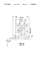
- FIG. 8 shows an exemplary conventional associative memory which is described in "MOS/LSI Design and Application” by W. N. Carr, J. P. Mize, pp. 222-225.
- each memory cell includes ten transistors T 1 -T 8 , T L1 and T L2 .
- the transistors T 1 -T 4 , T L1 and T L2 constitute a static RAM (random access memory), so that usual read/write operations can be performed.
- An associative memory action is performed in such a manner that the transistors T 5 -T 8 provide an exclusive-OR logic function between the voltage of the bit lines B(0) and B(1) and the node voltages Q and Q of a memory cell.
- the transistors T 6 and T 8 are both conducting (positive logic).
- the transistors T 5 and T 7 are both conducting.
- the associative memory can perform the matching of the data contents stored in memory cells which are arranged along the word line W with the reference data contents in the parallel fashion, whereby the processing speed can be improved. Due to such an advantage, associative memories are applied in various fields such as pattern recognition.
- the non-volatile memory cell of this invention includes: first and second selecting transistors, a gate of the first selecting transistor and a gate of the second selecting transistor being connected to a word line, a drain of the first selecting transistor being connected to a first bit line, a drain of the second selecting transistor being connected to a second bit line; first and second non-volatile memory transistors for storing data in a non-volatile manner, a drain of the first non-volatile memory transistor being connected to a source of the first selecting transistor, a drain of the second non-volatile memory transistor being connected to a source of the second selecting transistor, a source of the first non-volatile memory transistor and a source of the second non-volatile memory transistor being connected to a source line, a gate of the first non-volatile memory transistor and a gate of the second non-volatile memory transistor being connected to a control gate line; and first and second output transistors, a drain of the first output transistor and a drain of the second output transistor being connected to
- a non-volatile associative memory device including a plurality of memory cells.
- Each of the memory cells includes: first and second selecting transistors, a gate of the first selecting transistor and a gate of the second selecting transistor being connected to a word line, a drain of the first selecting transistor being connected to a first bit line, a drain of the second selecting transistor being connected to a second bit line; first and second non-volatile memory transistors for storing data in a non-volatile manner, a drain of the first non-volatile memory transistor being connected to a source of the first selecting transistor, a drain of the second non-volatile memory transistor being connected to a source of the second selecting transistor, a source of the first non-volatile memory transistor and a source of the second non-volatile memory transistor being connected to a source line, a gate of the first non-volatile memory transistor and a gate of the second non-volatile memory transistor being connected to a control gate line; and first and second output transistor
- a non-volatile memory transistor is of the floating gate type.
- the erase process is performed in the following manner. Predetermined voltages are applied to a common control gate line to which control gates of non-volatile memory transistors are connected, a word line to which gates of selecting transistors are connected, and a common source line, respectively. By this voltage application, electrons on floating gates of the non-volatile memory transistors are ejected into sources. Thus, the stored data is erased.
- the write process of data "1" or data "0” is performed in the following manner. Predetermined voltages are applied to two bit lines to which drains of the selecting transistors are respectively and separately connected, the common control gate line, the word line and the common source line, respectively. By this voltage application, electrons are injected into the floating gate of either one of the non-volatile memory transistors depending on the data "1” or "0" to be written. Thus, the data is written.
- the matching process is briefly described. For example, if the data stored in the non-volatile memory transistor match the reference data, a conduction path is formed between two common output lines which are respectively connected to output transistors. If the stored data and the reference data do not match, the conduction path is not formed between the two common output lines.
- the data of all the memory cells will be matched in a parallel fashion. If the match is perfect for all the memory cells, for example, "0" is output as a reference result output. If there is a mismatch even for one memory cell, "1" is output. That is, the matching operation for determining whether the data of memory cells match the reference data or not is performed in parallel fashion and at a high speed.
- the invention described herein makes possible the advantage of providing a non-volatile associative memory in which the size per unit memory cell can be made smaller and consequentially the capacity of the associative memory can be made larger and the production cost thereof can be lowered, and in which the data contents of the memory cells will not be volatilized when the voltage supply is turned OFF.
- FIG. 1 is a circuit diagram showing a memory cell in a non-volatile associative memory according to the present invention
- FIG. 2 is a diagram illustrating relationships between applied voltages and write/erase operations to the memory cell in the non-volatile associative memory according to the present invention
- FIG. 3 is a diagram illustrating relationships between written states of the memory cell and threshold voltages of non-volatile memory transistors
- FIG. 4 is a diagram showing the matching results of the memory cell states with reference data
- FIG. 5 is a circuit diagram showing the connection of a plurality of memory cells in the associative memory of the present invention corresponding to the matching results shown in FIG. 4;
- FIG. 6 is a diagram showing the matching results in a modified example of an associative memory of the present invention, in the same manner as in FIG. 4;
- FIG. 7 is a circuit diagram showing a connection of a plurality of memory cells in the modified example of the associative memory of the present invention corresponding to the matching results shown in FIG. 6;
- FIG. 8 is a circuit diagram showing a memory cell in an associative memory of the prior art.
- FIG. 1 shows a circuit configuration of a memory cell in a non-volatile associative memory according to the present invention.
- each memory cell includes six transistors Q 1 , Q 2 , Q 3 , Q 4 , Q 5 , and Q 6 .
- the transistors Q 1 , Q 4 , Q 5 , and Q 6 are N-channel MOS transistors.
- the transistors Q 2 and Q 3 are N-channel non-volatile memory transistors in which the stored data will not volatilize.
- the N-channel non-volatile memory transistors are of conventional floating gate type.
- Gates of the transistors Q 1 and Q 4 are connected to a word line W.
- a drain of the transistor Q 1 is connected to a bit line B.
- a drain of the transistor Q 4 is connected to a bit line B. Accordingly, the transistors Q 1 and Q 4 function as selecting transistors for selecting a memory cell M.
- a source of the transistor Q 1 is connected to a drain of the non-volatile memory transistor Q 2 .
- a source of the transistor Q 4 is connected to a drain of the non-volatile memory transistor Q 3 .
- Sources of the non-volatile memory transistors Q 2 and Q 3 are respectively connected to a common source line S.
- Gates of the non-volatile memory transistors Q 2 and Q 3 are respectively connected to a common control gate line CG.
- drains of the non-volatile memory transistors Q 2 and Q 3 are respectively connected to gates of the transistors Q 5 and Q 6 . Drains and sources of the transistors Q 5 and Q 6 are connected to common output lines R 1 and R 2 , respectively.
- the memory cell M is in the written state of data "1", and the reference data is "1", i.e., a case where the stored data matches the reference data.
- the bit line B is precharged to an "H” level, and the bit line B is at an "L” level. Accordingly, under these conditions, the transistors Q 1 , Q 4 and Q 5 and the non-volatile memory transistor Q 3 are in the ON state, and the non-volatile memory transistor Q 2 and the transistor Q 6 are in the OFF state, whereby a conduction path is formed between the common output lines R 1 and R 2 .
- the memory cell M is in the written state of data "1", and the reference data is "0", a case where the stored data and the reference data do not match.
- the bit line B is precharged to an "H” level, and the bit line B is at an "L” level. Accordingly, under these conditions, the transistors Q 1 and Q 4 and the non-volatile memory transistor Q 3 are in the ON state, and the non-volatile transistor Q 2 and the transistors Q 5 and Q 6 are in the OFF state, so the conduction path is not formed between the common output lines R 1 and R 2 .
- the memory cell M is in the written state of data "0", and the reference data is "1", i.e., a case where the stored data and the reference data do not match.
- the bit line B is precharged to the "H” level, and the bit line B is at the "L” level. Accordingly, under these conditions, the transistors Q 1 and Q 4 and the non-volatile memory transistor Q 2 are in the ON state, and the non-volatile memory transistor Q 3 and the transistors Q 5 and Q 6 are in the OFF state, so the conduction path is not formed between the common output lines R 1 and R 2 .
- the memory cell M is in the written state of data "0", and the reference data is "0", i.e., a case where the stored data matches the reference data.
- the bit line B is precharged to the "H” level, and the bit line B is at the "L” level. Accordingly, under these conditions, the transistors Q 1 , Q 4 and Q 6 and the non-volatile memory transistor Q 2 are in the ON state, and the non-volatile transistor Q 3 and the transistor Q 5 are in the OFF state, whereby the conduction path is formed between the common output lines R 1 and R 2 .
- the non-volatile associative memory of the invention if the written state of the memory cell M matches the reference data, a conduction path is formed between the common output lines R 1 and R 2 . If the written state and the reference data do not match, the conduction path is not formed between the common output lines R 1 and R 2 .
- a plurality of memory cells M are arranged into a line, and connected in a series manner via the common output lines R 1 and R 2 .
- the common output line R 2 of each memory cell is connected to the common output lines R 1 of adjacent memory cells.
- the common output line R 1 of the memory cell disposed at one end is connected to a supply voltage V CC .
- the common output line R 2 of the memory cell disposed at the other end is grounded.
- FIGS. 6 and 7 show a modified example of a non-volatile associative memory of the present invention.
- the reference data is inverted in the non-volatile associative memory and then the matching is performed with respect to the inverted reference data.
- the conduction path is not formed between the common output lines R 1 and R 2 .
- the conduction path is formed therebetween.
- FIG. 6 shows the matching result in the modified example
- FIG. 7 shows the connection of a plurality of memory cells.
- the common output lines R 1 of the respective memory cells M are connected to each other and the common output lines R 2 are also connected to each other.
- a plurality of memory cells M are connected in a parallel manner via the common output lines R 1 and R 2 .
- the common output line R 1 of each memory cell is connected to the common output lines R 1 of the adjacent memory cells.
- the common output line R 2 of each memory cell is connected to the common output lines R 2 of adjacent memory cells.
- the common output line R 1 of the memory cell is connected to a supply voltage V CC .
- the common output line R 2 of the memory cell is grounded.
- a single memory cell includes two selecting transistors for selecting the memory cell, two non-volatile memory transistors for storing data in a non-volatile manner, and two output transistors for outputting data. Accordingly, the size per unit memory cell can be remarkably reduced as compared with a memory cell including ten transistors in the conventional associative memory. Therefore, according to the non-volatile associative memory of the invention, the capacity of the associative memory can be increased and the associative memory can be produced at a much lower cost.
- non-volatile memory transistors are provided as data storing means, data in the memory cell will not volatilize even when the voltage supply is turned OFF.
- the matching operation of the contents of the memory cells with the reference data can be performed in a parallel fashion and at a high speed. Moreover, the matching degree can be detected.
- the non-volatile associative memory of the present invention is extremely useful industrially, because it is applicable to the pattern recognition field or the like.
Abstract
Description
Claims (8)
Applications Claiming Priority (2)
| Application Number | Priority Date | Filing Date | Title |
|---|---|---|---|
| JP4-49874 | 1992-03-06 | ||
| JP4049874A JP2798197B2 (en) | 1992-03-06 | 1992-03-06 | Non-volatile associative memory |
Publications (1)
| Publication Number | Publication Date |
|---|---|
| US5347483A true US5347483A (en) | 1994-09-13 |
Family
ID=12843197
Family Applications (1)
| Application Number | Title | Priority Date | Filing Date |
|---|---|---|---|
| US08/027,132 Expired - Lifetime US5347483A (en) | 1992-03-06 | 1993-03-05 | Non-volatile associative memory with low transistor count |
Country Status (2)
| Country | Link |
|---|---|
| US (1) | US5347483A (en) |
| JP (1) | JP2798197B2 (en) |
Cited By (6)
| Publication number | Priority date | Publication date | Assignee | Title |
|---|---|---|---|---|
| US5577051A (en) * | 1993-12-22 | 1996-11-19 | Sgs-Thomson Microelectronics, Inc. | Static memory long write test |
| EP1014382A1 (en) * | 1998-12-22 | 2000-06-28 | STMicroelectronics, Inc. | Floating gate content addressable memory |
| US20060285374A1 (en) * | 2005-06-16 | 2006-12-21 | Clement Szeto | Content addressable memory cell |
| CN100429670C (en) * | 2003-04-25 | 2008-10-29 | 三星电子株式会社 | Fingerprint identification system and method thereof |
| WO2010100000A1 (en) | 2009-03-06 | 2010-09-10 | International Business Machines Corporation | Ternary content addressable memory using phase change devices |
| US20140269063A1 (en) * | 2013-03-14 | 2014-09-18 | Semiconductor Energy Laboratory Co., Ltd. | Method for driving semiconductor device and semiconductor device |
Citations (9)
| Publication number | Priority date | Publication date | Assignee | Title |
|---|---|---|---|---|
| US4460978A (en) * | 1981-11-19 | 1984-07-17 | Mostek Corporation | Nonvolatile static random access memory cell |
| JPS63266697A (en) * | 1987-04-24 | 1988-11-02 | Hitachi Ltd | Contents access memory |
| JPH01184790A (en) * | 1988-01-18 | 1989-07-24 | Mitsubishi Electric Corp | Nonvolatile cam |
| JPH01192089A (en) * | 1988-01-28 | 1989-08-02 | Mitsubishi Electric Corp | Content address memory |
| JPH01194196A (en) * | 1988-01-28 | 1989-08-04 | Mitsubishi Electric Corp | Contents address memory |
| JPH01307095A (en) * | 1988-06-01 | 1989-12-12 | Mitsubishi Electric Corp | Nonvolatile cam |
| JPH0235690A (en) * | 1988-07-25 | 1990-02-06 | Mitsubishi Electric Corp | Non-volatile associative storage memory and its data writing method |
| JPH0278098A (en) * | 1988-02-23 | 1990-03-19 | Mitsubishi Electric Corp | Content reference memory cell |
| US5051948A (en) * | 1988-02-23 | 1991-09-24 | Mitsubishi Denki Kabushiki Kaisha | Content addressable memory device |
-
1992
- 1992-03-06 JP JP4049874A patent/JP2798197B2/en not_active Expired - Fee Related
-
1993
- 1993-03-05 US US08/027,132 patent/US5347483A/en not_active Expired - Lifetime
Patent Citations (9)
| Publication number | Priority date | Publication date | Assignee | Title |
|---|---|---|---|---|
| US4460978A (en) * | 1981-11-19 | 1984-07-17 | Mostek Corporation | Nonvolatile static random access memory cell |
| JPS63266697A (en) * | 1987-04-24 | 1988-11-02 | Hitachi Ltd | Contents access memory |
| JPH01184790A (en) * | 1988-01-18 | 1989-07-24 | Mitsubishi Electric Corp | Nonvolatile cam |
| JPH01192089A (en) * | 1988-01-28 | 1989-08-02 | Mitsubishi Electric Corp | Content address memory |
| JPH01194196A (en) * | 1988-01-28 | 1989-08-04 | Mitsubishi Electric Corp | Contents address memory |
| JPH0278098A (en) * | 1988-02-23 | 1990-03-19 | Mitsubishi Electric Corp | Content reference memory cell |
| US5051948A (en) * | 1988-02-23 | 1991-09-24 | Mitsubishi Denki Kabushiki Kaisha | Content addressable memory device |
| JPH01307095A (en) * | 1988-06-01 | 1989-12-12 | Mitsubishi Electric Corp | Nonvolatile cam |
| JPH0235690A (en) * | 1988-07-25 | 1990-02-06 | Mitsubishi Electric Corp | Non-volatile associative storage memory and its data writing method |
Non-Patent Citations (2)
| Title |
|---|
| Carr, W. N. et al., MOS/LSI Design and Application Texas Instrument Electronics Series, Holliday Lithograph Corp. (1972) pp. 222 225. * |
| Carr, W. N. et al., MOS/LSI Design and Application Texas Instrument Electronics Series, Holliday Lithograph Corp. (1972) pp. 222-225. |
Cited By (8)
| Publication number | Priority date | Publication date | Assignee | Title |
|---|---|---|---|---|
| US5577051A (en) * | 1993-12-22 | 1996-11-19 | Sgs-Thomson Microelectronics, Inc. | Static memory long write test |
| EP1014382A1 (en) * | 1998-12-22 | 2000-06-28 | STMicroelectronics, Inc. | Floating gate content addressable memory |
| CN100429670C (en) * | 2003-04-25 | 2008-10-29 | 三星电子株式会社 | Fingerprint identification system and method thereof |
| US20060285374A1 (en) * | 2005-06-16 | 2006-12-21 | Clement Szeto | Content addressable memory cell |
| WO2010100000A1 (en) | 2009-03-06 | 2010-09-10 | International Business Machines Corporation | Ternary content addressable memory using phase change devices |
| CN102341863A (en) * | 2009-03-06 | 2012-02-01 | 国际商业机器公司 | Ternary content addressable memory using phase change devices |
| US20140269063A1 (en) * | 2013-03-14 | 2014-09-18 | Semiconductor Energy Laboratory Co., Ltd. | Method for driving semiconductor device and semiconductor device |
| US9171630B2 (en) * | 2013-03-14 | 2015-10-27 | Semiconductor Energy Laboratory Co., Ltd. | Method for driving semiconductor device and semiconductor device |
Also Published As
| Publication number | Publication date |
|---|---|
| JPH05250879A (en) | 1993-09-28 |
| JP2798197B2 (en) | 1998-09-17 |
Similar Documents
| Publication | Publication Date | Title |
|---|---|---|
| US4965767A (en) | Associative memory having simplified memory cell circuitry | |
| US5111427A (en) | Nonvolatile content-addressable memory and operating method therefor | |
| USRE39227E1 (en) | Content addressable memory (CAM) arrays and cells having low power requirements | |
| US5608667A (en) | Ferroelectric memory automatically generating biasing pulse for plate electrode | |
| US4745579A (en) | Electrically erasable programmable logic array (EEPLA) | |
| US4813018A (en) | Nonvolatile semiconductor memory device | |
| US4831585A (en) | Four transistor cross-coupled bitline content addressable memory | |
| US6373739B1 (en) | Quad CAM cell with minimum cell size | |
| EP1376607B1 (en) | Content addressable memory device and method of operating same | |
| KR950013393B1 (en) | Semiconductor integrated circuit | |
| US5402382A (en) | Nonvolatile semiconductor memory device capable of erasing by a word line unit | |
| US6845025B1 (en) | Word line driver circuit for a content addressable memory | |
| CA2068862A1 (en) | Semiconductor integrated circuit | |
| US6388909B2 (en) | Associative memory for accomplishing longest coincidence data detection by two comparing operations | |
| JP2947825B2 (en) | Integrated semiconductor circuit | |
| US5347483A (en) | Non-volatile associative memory with low transistor count | |
| JPH0612884A (en) | Associative storage device | |
| US4799192A (en) | Three-transistor content addressable memory | |
| US6055189A (en) | Nonvolatile semiconductor memory device | |
| US3986054A (en) | High voltage integrated driver circuit | |
| US5239207A (en) | Semiconductor integrated circuit | |
| US20040109338A1 (en) | Ternary content addressable memory cell | |
| US5101379A (en) | Apparatus for page mode programming of an EEPROM cell array with false loading protection | |
| KR102481452B1 (en) | NOR Type Content Addressable Memory Cell Based on Ferroelectric Element and Content Addressable Memory Including Same | |
| JP2605595B2 (en) | Associative memory |
Legal Events
| Date | Code | Title | Description |
|---|---|---|---|
| AS | Assignment |
Owner name: SHARP KABUSHIKI KAISHA, JAPAN Free format text: ASSIGNMENT OF ASSIGNORS INTEREST;ASSIGNOR:TORIMARU, YASUO;REEL/FRAME:006539/0584 Effective date: 19930414 |
|
| STCF | Information on status: patent grant |
Free format text: PATENTED CASE |
|
| FEPP | Fee payment procedure |
Free format text: PAYOR NUMBER ASSIGNED (ORIGINAL EVENT CODE: ASPN); ENTITY STATUS OF PATENT OWNER: LARGE ENTITY |
|
| FPAY | Fee payment |
Year of fee payment: 4 |
|
| FPAY | Fee payment |
Year of fee payment: 8 |
|
| FPAY | Fee payment |
Year of fee payment: 12 |
|
| AS | Assignment |
Owner name: INTELLECTUAL PROPERTIES I KFT., HUNGARY Free format text: ASSIGNMENT OF ASSIGNORS INTEREST;ASSIGNOR:SHARP KABUSHIKI KAISHA;REEL/FRAME:027387/0650 Effective date: 20111115 |
|
| AS | Assignment |
Owner name: SAMSUNG ELECTRONICS CO., LTD, KOREA, REPUBLIC OF Free format text: ASSIGNMENT OF ASSIGNORS INTEREST;ASSIGNOR:INTELLECTUAL PROPERTIES I KFT.;REEL/FRAME:035120/0878 Effective date: 20141222 |
|
| AS | Assignment |
Owner name: SAMSUNG ELECTRONICS CO., LTD., KOREA, REPUBLIC OF Free format text: CORRECTIVE ASSIGNMENT TO CORRECT THE ASSIGNEE NAME PREVIOUSLY RECORDED AT REEL: 035120 FRAME: 0878. ASSIGNOR(S) HEREBY CONFIRMS THE ASSIGNMENT;ASSIGNOR:INTELLECTUAL PROPERTIES I KFT.;REEL/FRAME:035837/0619 Effective date: 20141222 |