US5359727A - Clock generator using PLL and information processing system using the clock generator - Google Patents
Clock generator using PLL and information processing system using the clock generator Download PDFInfo
- Publication number
- US5359727A US5359727A US07/487,125 US48712590A US5359727A US 5359727 A US5359727 A US 5359727A US 48712590 A US48712590 A US 48712590A US 5359727 A US5359727 A US 5359727A
- Authority
- US
- United States
- Prior art keywords
- signal
- current
- frequency
- clock
- circuit
- Prior art date
- Legal status (The legal status is an assumption and is not a legal conclusion. Google has not performed a legal analysis and makes no representation as to the accuracy of the status listed.)
- Expired - Lifetime
Links
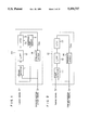
Images


Classifications
-
- G—PHYSICS
- G06—COMPUTING; CALCULATING OR COUNTING
- G06F—ELECTRIC DIGITAL DATA PROCESSING
- G06F1/00—Details not covered by groups G06F3/00 - G06F13/00 and G06F21/00
- G06F1/04—Generating or distributing clock signals or signals derived directly therefrom
- G06F1/10—Distribution of clock signals, e.g. skew
Definitions
- the present invention relates generally to a clock generator, and more specifically, to a clock generation circuit for a semiconductor integrated circuit device including an information processing system in which logic operations are carried out based upon the clock.
- JP-A-55-80137 corresponding to U.S. Pat. No. 4,419,739 which discloses a circuit for generating a clock synchronized with an external signal.
- IEEE JOURNAL OF SOLID-STATE CIRCUITS SC-22 No. 2 (1987) pages 255 to 261, and JP-A-58-184626 show examples of clock generating circuit employing a phase-locked loop (simply referred to as a "PLL").
- FIG. 2 is a schematic block diagram of a clock generating circuit employing such a PLL, as disclosed in U.S. Pat. No. 5,133,064, issued on Jul. 21, 1992.
- a clock generating circuit 10 is formed of a phase detector 11, a low-pass filter (LPF) 12, a voltage controlled oscillator (VCO) 13, and a frequency divider 14.
- the phase detector 11 continuously compares the phase difference between a timing signal related to an external signal and a synchronization clock signal.
- the output produced by the phase difference is smoothed by LPF 12 and supplied as a control signal for VCO 13.
- VCO 13 increases/decreases an oscillating frequency in response to the supplied output from LPF 12, an oscillating output is frequency-divided by a frequency divider 14 and then is outputted as a synchronization clock signal.
- These circuits constitute a feedback system.
- the phase detector 11 detects the phase difference therebetween and causes the oscillating frequency of VCO 13 to increase via LPF 12.
- the oscillating frequency of VCO 13 is increased, the frequency of the synchronization clock signal is also increased so that the phase of the synchronization clock signal leads and the phase difference between the synchronization clock signal and the timing signal is decreased.
- PLL 10 operates to synchronize the phase of the synchronization clock signal with that of the timing signal and also to make both frequencies coincident, which functions as an automatic frequency control.
- circuits 11 to 14 have been hitherto proposed as circuit elements forming PLL 10, which are selectively utilized taking account of a desired overall performance.
- JP-A-60-128709 Japanese Patent Application No. 58-237228
- VCO 13 a capacitor (e.g., a stray capacitance) is employed therein, a charging/discharging current thereof is controlled in response to an input voltage, whereby a time constant is varied so as to determine the oscillating frequency.
- the charging/discharging current of the capacitor may be varied within a predetermined range.
- a variable range of the oscillating frequency is necessarily restricted to a predetermined range.
- PLL 10 Since PLL 10 is so operated as to make the phase of the timing signal coincident with that of the synchronization clock signal, there is a case where the phase of the timing signal is coincident with that of the synchronization clock signal even when the frequency of the synchronization clock signal is equal to a frequency produced by multiplying the frequency of the timing signal by an integral number or an inverse number. In this case, since there is no phase difference between these signals, PLL 10 is brought into a balanced condition, and thus a quasi phase-locked state may occur. To avoid this difficulty, the oscillating frequency of VCO 13 employed in PLL 10 must be limited to a predetermined range over which no quasi phase-locked state occurs.
- the variable range of the oscillating frequency of VCO 13 is set to a predetermined range.
- each of the information processing sections employed in the system is operated at a high speed.
- the semiconductor integrated circuit can be operated at the clock frequency of 30 MHz.
- a report has been made that such a circuit is operable at the frequency higher than 70 MHz by utilizing Bi CMOS techniques. Then, these semiconductor integrated circuits are not only operated at the maximum frequency, but also operated even at a frequency lower than this maximum frequency.
- a diagnostic circuit additionally provided for the testing purpose must operate at a frequency, for instance, which is several MHz lower than the usual operation frequency of the normal logic circuits.
- clock generating circuits included in respective information processing systems are preferably operable under the input or timing clock frequencies from several MHz to several tens MHz.
- the input clock frequency range of the clock generating circuit is narrow, there is a possibility of incapability of the desired operation of the clock generating circuit when the operating frequency must be varied due to the testing operation. As a consequence, it is required to additionally employ an exclusive clock generating circuit in response to such a variable frequency range of the input timing frequency. Otherwise, means for externally adjusting the operating range of the clock generating circuit must be provided, and the adjustments must be made for every circuit in correspondence with the desired frequencies.
- a principal object of the present invention is to provide a clock generator having a wide frequency range (e.g., in the order of 1 to 100 MHz) and capable of generating a synchronization clock signal in response to an externally inputted timing signal whose frequency may be varied in a wide range.
- a clock generator having a wide frequency range (e.g., in the order of 1 to 100 MHz) and capable of generating a synchronization clock signal in response to an externally inputted timing signal whose frequency may be varied in a wide range.
- Another object of the present invention is to provide a clock generating apparatus wherein a PLL is employed and a clock signal synchronized with an input timing signal is generated, and further there is provided compensation means for varying an oscillating frequency range of voltage controlled oscillating means in the PLL in response to a frequency variation of the input timing signal.
- Another object of the present invention is to provide an information processing system employing a plurality of information processing sections and clock generating means for these sections which are synchronized with one another.
- Another object of the present invention is to provide a clock generating apparatus wherein a plurality of clock signals synchronized with an input timing signal are produced and distributed by employing PLL, one clock signal distributed from the distributing circuit is inputted to the phase detector employed in the PLL so as to phase-compare the clock signal with the input timing signal.
- Another object of the present invention is to provide an information processing system comprising a plurality of information processing sections provided with the clock generating apparatuses to establish a synchronization between the sections.
- a further object of the present invention is to provide a charge pump circuit suitable for a low-pass filter of a PLL type clock generating apparatus including compensation means for varying an oscillating frequency range of voltage controlled oscillating means employed in the PLL in response to a frequency variation in an input timing signal; and to provide a frequency/current converting means suitable as the compensation means.
- a clock generating apparatus which includes phase comparing means; voltage controlled oscillating means for generating an oscillation output signal having a frequency in response to an output signal of the phase comparing means; means for generating a clock signal based upon the oscillation output from the voltage controlled oscillating means, an input timing signal and the generated clock signal being inputted to the phase comparing means so as to generate a clock signal synchronized with the input timing signal; and compensation means for receiving the input timing signal and varying a range of an oscillating frequency of the voltage controlled oscillating means in response to a frequency variation of the input timing signal.
- the compensation means When the frequency of the timing signal is high, the compensation means varies the range of the oscillating frequency of the voltage controlled oscillating means to a higher frequency range. As a result, since the frequency range of the synchronization clock signal in the clock generating apparatus is similarly changed into a higher frequency range, it can be prevented that the frequency of the timing signal is out of the frequency range of the synchronization clock signal. Conversely, when the frequency of the timing signal is lowered the compensation means operates so as to change the frequency range of the synchronization clock signal into a lower frequency range.
- the clock generating apparatus since the frequency range of the synchronization clock signal is varied in accordance with the frequency change of the timing signal, it can obviate the conventional inconvenience that the clock generating apparatus gets in failure due to the incapability of following the frequency changes in the timing signal.
- the clock generating apparatus having the wide frequency range of the input clock can be realized. As a result, clock generating circuits exclusively used for the frequency of various input clocks are no longer required, and also conventional adjustments for clock generating circuits are no longer required.
- the synchronization clock signal based upon the output of the voltage controlled oscillating means can be reliably synchronized with the timing signal.
- the operations relating to the data processing including data transfer operations between a plurality of information processing apparatuses can be reliably synchronized with each other.
- various types of semiconductor device testing apparatuses operable at different frequencies can be realized.
- Other practical examples of applying the present invention are information processing systems such as office computers, work stations which operate at high frequencies with logic LSIs requiring synchronization of internal clock signals, and portable type personal computers with a power-saving capability of lowering their operating frequency to decrease their power loss in the case where there is no accessing of the system elements.
- the frequency decreasing operation is included for the saving of necessary electric power as one of the cases of changing operating frequencies of such LSI-incorporated systems.
- Chip operating electric power is approximately proportional to operating frequency in CMOS or BiCMOS LSIs.
- FIG. 1 is a schematic block diagram of a clock generating circuit according to one embodiment of the present invention
- FIG. 2 is a schematic block diagram of a clock generating circuit of U.S. Pat. No. 5,133,064;
- FIG. 3 is a schematic block diagram of a semiconductor integrated circuit device employing the embodiment shown in FIG. 1;
- FIG. 4 is a schematic block diagram of a clock generating circuit according to another embodiment of the present invention.
- FIG. 5 is a schematic block diagram of a semiconductor integrated circuit device employing the embodiment shown in FIG. 4;
- FIG. 6 is a schematic block diagram of an information processing system employing a clock generating circuit according to the present invention.
- FIG. 7 is a circuit arrangement of a phase detector
- FIG. 8 is a timing chart for explaining an operation of the phase detector
- FIG. 9 is a circuit diagram of a low-pass filter according to the present invention.
- FIG. 10 is a schematic block diagram of an overall arrangement of a voltage controlled oscillator
- FIGS. 11 through 13 are detailed circuit diagrams for explaining various parts of the voltage controlled oscillator shown in FIG. 10;
- FIG. 14 is a circuit arrangement of a frequency divider
- FIG. 15 is a circuit arrangement of a compensation circuit according to the present invention.
- FIG. 16 is a timing chart for explaining an operation of the compensation circuit shown in FIG. 15;
- FIG. 17 is a schematic arrangement of a capacitor for determining an oscillating frequency according to the present invention.
- FIGS. 18A and 18B illustrate structures of the capacitor shown in FIG. 17 on a semiconductor chip
- FIG. 19 is an equivalent circuit of the capacitor shown in FIG. 18.
- FIG. 1 shows a schematic block diagram of a first embodiment according to the present invention.
- a compensation circuit 15 is provided for receiving a timing signal "S T " as an input and for varying an oscillating frequency range of VCO13 in response to a timing frequency "f T " of the signal S T .
- the compensation circuit 15 outputs a signal "S C " for enabling the oscillating frequency range of VCO13 to be changed into a higher frequency range when the frequency f T is increased.
- the compensation circuit 15 outputs another signal S C to VCO13, whereby the oscillating frequency range is shifted to a lower frequency range.
- a synchronization clock signal C P corresponds to a signal which is obtained by frequency-dividing an oscillating output signal C PO of VCO13 in a frequency divider 14.
- the frequency range of the synchronization clock signal C P has a proportional relationship with the oscillating frequency range of VCO13.
- the frequency f T is within the frequency range of the synchronization clock signal C P .
- the present embodiment can realize a clock generating circuit having such a wide frequency range as being capable of following the variations in the frequency of the timing signal S T . It is noted that specific embodiments of VCO13 and compensation circuit 15 will be discussed later (FIGS. 10, 11 and 15).
- FIG. 3 shows an arrangement of an information processing LSI chip in which the clock generating circuit 20 shown in FIG. 1 is incorporated.
- the LSI chip 310 is formed of a clock circuit 20 comprising a clock generating circuit (CPG)20 and a clock distributing circuit 21, and of logic circuit blocks 311 to 315 under the control of the clock signal C P outputted from the clock circuit 22.
- CPG20 In response to the timing signal S T inputted from the outside of the chip, CPG20 outputs the synchronization clock signal C P synchronized with the timing signal and produces at the distributing circuit 21 a clock signal for controlling the respective blocks 311 to 315.
- the clock signal C P corresponds to a signal which is delayed from the timing signal S T by a delay time caused in the distributing circuit 21.
- the LSI chip 310 is operated substantially in synchronization with the timing signal. As a result, when the LSI chip 310 transmits and receives data via a local bus 10 and a system bus 102, there is a particular advantage that the LSI chip 310 can be operated in the synchronization mode based upon the timing signal used commonly with other systems.
- FIG. 4 an arrangement of a second embodiment according to the present invention is shown.
- the same reference numerals employed in FIGS. 1 and 2 indicate the same functions and arrangements.
- a different point from the above-described embodiment shown in FIG. 1 is such an arrangement that one of the clock signals C P is fed back to the phase detector 11 via the clock distributing circuit 21 for distributing the outputs of the frequency divider 14.
- the delays caused by the clock distributing circuit 21 can be also compensated, and the clock signals of the logic blocks 311 to 315 as described with reference to FIG. 3 can be synchronized with the external timing signal S T .
- the above-described delays by the distributing circuit 21 are caused by employing a multiplicity of buffers for the distribution purpose. The typical delay is, for instance, 2 to 3 n sec.
- FIG. 5 shows an arrangement of an information processing chip according to another embodiment of this invention, in which the clock circuit 25 shown in FIG. 4 is incorporated.
- the same reference numerals shown in FIG. 3 indicate the same components.
- the LSI chip 310 is operated in synchronization with the timing signal, and is operable in a complete synchronization mode while transmitting and receiving data via local bus 101 and system bus 102 to other LSI chips.
- FIG. 6 shows an information processing system according to still another embodiment employing the information processing LSI shown in FIG. 3 or 5.
- reference numeral 310 indicates CPU (central processing unit) for processing information in accordance with a program
- reference numeral 320 denotes MMU (memory management unit) for managing data processed in the system and storing a portion of the data as a cache memory
- reference numeral 330 represents FPU (floating processing unit) in which a numeral calculation required for a software processing operation is performed at a high speed by employing an exclusive hardware.
- the respective units 310 to 330 are connected via a system bus 102 to each other and to other peripheral portions.
- An inherent local bus 101 is provided to connect the unit 310 to the unit 320 so that the unit 310 can access the cache memory employed in the unit 320 at a high speed.
- the respective units 310 to 330 include clock circuit 22 or 25 which are controlled by a common timing signal "S T " outputted from a timing signal generating circuit 40.
- S T a common timing signal
- all of clock signals to control logic blocks employed in the units 310 to 330 are in synchronism with each other, the synchronization of the data transfer effected between the LSIs via the data buses 101 and 102 can be established, and thus the data transfer can be surely performed.
- the high speed operation can be realized and the high-speed information processing system can be accordingly obtained.
- FIGS. 7 to 16 concrete embodiments of the respective block units for constituting the embodiments shown in FIGS. 1 and 4 will be described.
- phase detector 11 As shown in the figure, the phase detector 11 is formed of inverters 701, 702, 712 to 715; 2-input NANDs 703 to 708; 3-input NANDs 710, 711; and 4-input NAND 709.
- the phase detector with this arrangement is a frequency/phase comparing type phase comparator for converting a phase difference between leading edges of the timing signal S T and synchronization clock signal C P into output pulse signals PP, NP, PD and ND having waveforms shown in a timing chart of FIG. 8 with respective pulse widths.
- Level-inverted pulses are outputted by the inverters 714 and 715.
- pulse signals PP and NP having pulse widths corresponding to the phase differences are outputted.
- FIG. 9 shows a low-pass filter (LPF) 12 according to the present invention.
- LPF low-pass filter
- a charge pump circuit 901 and a loop filter 917 are employed so as to form the low-pass filter.
- reference numerals 904 to 907 indicate PMOS
- reference numerals 908 to 916 indicate NMOS
- reference numeral 902 is a resistor
- reference numeral 903 indicates an NPN transistor.
- the charge pump circuit 901 is designed so that each current flowing through PMOS 906, 907 and NMOS 909, 910 is equal to each other. That is to say, PMOSs 904 and 906, 904 and 907, PMOSs 904 and 905, NMOS 908 and 909, and 908 and 910 constitute current mirrors, and then their currents are controlled by the current flowing through the resistor 902 by the bias voltage "V A " of the transistor 903.
- NMOSs 912, 911 and NMOSs 914, 913 are controlled by the opposite polarity output pulse signals PP, NP and PD, ND of the phase detector 11. These NMOSs 912, 911 and NMOSs 914, 913 are switches for switching the currents flowing through PMOS 907 and NMOS 910 between into an injection current to the output V B and into an internal sink or absorption current.
- NMOS 912 when NMOS 912 is turned on, the signal PP is "H” and the signal NP is "L”, the current of PMOS 907 is supplied to the output V B .
- NMOS 916 is controlled in response to the signal NP and turned on when NMOS 912 is turned off, when as shown in FIG. 8, the signal PP is "L” and the signal NP is "H".
- the current of PMOS 907 is conducted to NMOS 909 via the NMOS 916 and NMOS 911 which is also turned on.
- NMOS 915 is controlled by the signal ND and turned on when NMOS 914 is turned off. That is to say, in case that the signal PD is "L” and the signal ND is "H”, NMOS 914 is turned on, and the current of PMOS 906 is conducted to NMOS 910 via NMOS 915 and NMOS 913 which is also turned on.
- the loop filter 917 is formed of a series circuit comprising a resistor 918 and a capacitor 919, and integrates a pulse current of the charge pump circuit 901 to be converted into a voltage.
- the charge pump circuit 901 injects charges into the loop filter 917 with the output pulse signals PP and NP, the potential of V B is increased. Since the charge pump circuit 901 draws charges from the loop filter 917 with the output pulse signals PD and ND, the potential of V B is decreased. As a consequence, the pulse signal corresponding to the phase difference is converted into the voltage.
- FIG. 10 there is shown a voltage controlled oscillator (VCO) 13 according to still another embodiment.
- the voltage controlled oscillator 13 is formed of a voltage/current converting circuit 1001, a current controlled oscillator 1002 and a level converting circuit 1003.
- the voltage/current converting circuit 1001 converts the output voltage V B of the low-pass filter 12 into a current control signal I D and outputs this current control signal I D to the current controlled oscillator 1002 in response to a current control signal I C to a compensating circuit 15.
- the current controlled oscillator 1002 oscillates at a frequency corresponding to the current control signal I D , and outputs a signal V E (ECL level) having a low voltage amplitude.
- the level converting circuit 1003 amplifies V E to a signal V F having a CMOS level and outputs the same.
- FIG. 11 shows the voltage/current converting circuit 1001 shown in FIG. 10 according to yet another embodiment.
- NMOSs 1101, 1102 and 1103 constitute a current mirror.
- Currents I 1 and I 2 flowing through NMOSs 1102 and 1103 respectively have a proportional relationship with a current I C , and are expressed by the following equations:
- NMOSs 1104 and 1105 constitute a differential pair, and shunts the current I 1 in accordance with a potential relationship between a reference voltage V R and a voltage V B .
- the current of NMOS 1104 flows through PMOS 1106.
- This PMOS 1106 and another PMOS 1107 constitute a current mirror, and when currents flowing therethrough are set to be equal to each other, the current of PMOS 1107 is equal to that of NMOS 1104.
- V B is higher than that of V R
- NMOS 1105 becomes higher than that of NMOS 1104.
- PMOS 1107 can supply only the same current as that of NMOS 1104, the difference thereof between the currents of NMOS 1105 and 1104 is supplied from the circuit of PMOS 1108 and NMOS 1103. As a consequence, a current I 3 flowing through PMOS 1108 is higher than another current I 2 flowing through NMOS 1103. Conversely, in case that the potential of V B is lower than that of V R , the current flowing through NMOS 1105 is lower than that of NMOS 1104, but PMOS 1107 supplies the same current as that of NMOS 1104, so that an extra current other than a current flowing through NMOS 1105 is directed into the circuit of NMOS 1108 and NMOS 1103 and the current I 3 is lower than the current I 2 .
- the current I 3 is varied with a center of I 2 in response to the amplitudes of the voltage V B .
- a variation range of the current I 3 is determined by the following relation under the condition of the bias current I 1 of NMOSs 1104 and 1105.
- the voltage/current converting circuit 1001 is operated in such a way that when the potential of the output voltage V B becomes high within the range where the relation (5) is satisfied, then the current I D becomes large, whereas the current I D becomes small when the potential of the output voltage V B becomes low. Also, the range where the current I D is changed depends upon the current I C . When the current I C is set to be large, the center of the range of the current "I D " is moved to a large value. Conversely, when the current I C is set to be small, the center thereof is moved to a small value.
- FIG. 12 shows a current controlled oscillator 1002.
- the oscillator 1002 includes: NMOSs 1201 to 1203; a capacitor 1204; NPN transistors 1205, 1206, 1211, 1212; PMOSs 1207, 1208; diodes 1209, 1210, and current sources 1213, 1214.
- This oscillator 1002 corresponds to an emitter-coupled type multivibrator having such an arrangement that the input/output of switching circuit formed of bipolar transistors 1205, 1206, and PMOSs 1207, 1208 as load elements, are cross-coupled to each other via respective level shift circuits formed of transistor 1211 and current source 1213, and also of transistor 1212 and current source 1214.
- NMOSs 1201, 1202 and 1203 constitute a current mirror. As a result, when currents flowing through NMOSs 1202 and 1203 are set to "I 4 ", this current I 4 has a proportional relationship with the output current I D of the voltage/current converting circuit 1001, and is expressed by the following equation:
- the oscillating frequency "f o " of such an emitter coupled type multivibrator is expressed by the following equation if the capacitance of the timing capacitor 1204 is equal to C O ": ##EQU1## Based upon the above equations (6) and (7), the following relation can be obtained: ##EQU2## That is to say, the current controlled oscillator 1002 outputs the oscillating frequency proportional to the current I D .
- the oscillating frequency "f O " has a frequency range and the following relations is satisfied based upon the relations (5) and (8): ##EQU3## As apparent from the foregoing explanation, when the current I C becomes large, a center of the frequency range of the oscillating frequency "f O " is moved to a higher frequency. Conversely, when the current I C becomes small, this center is moved to a lower frequency.
- a switching circuit is arranged by the switching elements of NPN transistors 1205 and 1206, and PMOS transistors 1207 and 1208 as load elements, and further the gates of the PMOS transistors 1207 and 1208 are connected to the base electrodes of the NPN transistors 1205 and 1206, respectively.
- the base potential of the NPN transistor 1205 becomes high when the NPN transistor 1205 is turned on, the gate voltage of the PMOS transistor 1207 becomes low and its impedance becomes high.
- the NPN transistor 1205 is turned off, since the base potential thereof becomes low, the gate voltage of the PMOS transistor 1207 becomes high and its impedance becomes low. This is similarly applied to the relationship between the NPN transistor 1206 and PMOS transistor 1208.
- the impedances of the load elements 1207 and 1208 become high when the switching elements 1205 and 1206 are turned on, respectively, the voltage drop becomes large even when the current is small, and also the respective voltage amplitude to be limited by the clamp elements 1209 and 1210 can be procured.
- the impedances of the load elements 1207 and 1208 become low when the switching elements 1205 and 1206 are turned off, the collector voltages of the switching elements 1205 and 1206 can be quickly increased to the power source voltage. In current controlled oscillators where such load elements have a constant or fixed impedance value, the oscillating bandwidth becomes narrow.
- the oscillating frequency becomes low, that is to say, the current flowing through the switching element is small
- the voltage drop at the load element becomes small in proportion to the current.
- the output amplitude as the oscillator cannot be maintained, so that no operation is made.
- the oscillating frequency becomes high, there is no problem in the output amplitude.
- the rising speed of the output is determined by a time constant defined by the impedance of the load element and a stray capacitance to be driven by this element, no operation is made at a higher frequency than the frequency determined by this time constant.
- the oscillator having the wide oscillating frequency range can be realized by varying the impedance of the load element.
- FIG. 13 there is shown a level converting circuit 1003 according to a further embodiment. As shown in FIG. 13, this level converting circuit 1003 is constructed of PMOSs 1301, 1302, 1304, 1306, 1308, 1309, 1312 and 1313, and NMOSs 1303, 1305, 1307, 1310, 1311, 1314 and 1315.
- MOSs 1305 and 1307 functioning as bias current sources for ratio type inverter circuits arranged by MOSs 1304, 1305; and 1306, 1307 are controlled by outputs of a circuit constructed of MOSs 1301 to 1303 to which the output pulse signals V E of the current controlled oscillator 1002 are inputted, a logic threshold value of the ratio type inverter circuit can be set at a center of the high and low levels of the pulse signal V E , so that the circuit arranged by MOSs 1301 to 1307 can surely amplify the amplitude of the pulse signal V E .
- the circuit formed of MOSs 1308 through 1311 and MOSs 1312 to 1315 corresponds to a push-pull type inverter circuit arranged by a CMOS type current mirror, and further amplifies the amplified pulse signal to a signal having a CMOS level amplitude via the single-ended circuit.
- the level converting circuit 1003 is a double-amplification circuit by which the low voltage pulse signals V E of the current controlled oscillator 1002 are level-changed to two level-increased output pulse signals "V F " of a CMOS level and of opposite polarities at which the logic gate circuit can be operated.
- FIG. 14 shows a frequency divider 14.
- the frequency divider 14 includes feedback type latch circuits 1401 and 1402 formed of clocked inverter gate circuits 1404, 1406, 1407 and 1409, and inverter gate circuits 1405 and 1408. These are controlled in an opposite logic level in response to the output pulse signals V F of the level converting circuit and negatively fed back via an inverter gate circuit 1403 so as to divide the frequency of the output pulse signals V F by 2 and to output the frequency-divided output signal as a synchronization clock signal C P .
- FIG. 15 there is shown a compensation circuit 15 according to a still further embodiment.
- the frequency divider 1501 outputs an output signal "a 1 " which is obtained by dividing the frequency "f T " of the timing signal "S T " by 2.
- This signal a 1 is supplied to the gates of PMOS 1503 and NMOS 1504 so as to control a charging/discharging operation of a capacitor 1505, which constitutes an integrator circuit.
- a potential a 2 of this capacitor 1505 is applied to a plus input terminal of a comparator 1510.
- a potential "a 3 " of 3 VBE is applied from a bias circuit arranged by a series circuit including a current source 1506 and diodes 1507 to 1509.
- the comparator 1510 compares the input potentials a 2 with a 3 so as to thereby output an output signal a 4 having a CMOS level amplitude.
- This signal a 4 is inputted to gates of PMOS 1512 and NMOS 1513. These switching elements are series-connected to each other in order to constitute a charge pump circuit.
- An output signal a 5 of this charge pump circuit is supplied to a capacitor 1515 so that a charging/discharging operation of the capacitor 1515 is controlled.
- the output signal a 5 is applied to a low-pass filter arranged by a resistor 1516 and a capacitor 1517 so as to smooth the potential of the capacitor 1515.
- An output voltage "a 6 " of the low-pass filter circuit is applied to a gate of NMOS 1518.
- This NMOS 1518 is connected to PMOS 1519 of a current mirror circuit formed of PMOSs 1502, 1519 and 1520.
- a current I 8 flowing through NMOS 1518 in response to the signal a 6 an output current I c flowing through PMOS 1520 of the compensation circuit 15, and a charging circuit I 5 of the capacitor 1505 are made in proportion to each other.
- FIG. 16 there is shown a timing chart of potentials of various circuit portions of the compensation circuit 15.
- the timing signals "a 1 " and “a 4 " represent logic levels.
- a current flowing through PMOS 1502 is “I 5 "; currents flowing through current sources 1511 and 1514 are I 6 and I 7 respectively; a current flowing through PMOS 1519 and 1518 is “I 8 "; capacitances of capacitors 1505 and 1515 are C 1 and C 2 ; and a frequency of a timing signal S T is f T , a time period "t 0 " thereof is expressed as follows: ##EQU4##
- the signal a 1 corresponds to an output obtained by frequency-dividing the timing signal S T by 2 in the frequency divider 1501
- this signal is a signal having a duty ratio of 50%, and is equal to "t 0 " during periods of "H” and "L".
- the potential of the signal a 2 is increased at a gradient of I 5 /C 1 since the capacitor 1505 is charged via PMOS 1503 and PMOS 1502 when the signal a 1 is at an "L" level.
- NMOS 1504 quickly discharges the capacitor 1505 to a ground level.
- the signal a 4 becomes “L” when the signal a 2 is higher than the signal a 3 since the comparator 1510 compares the potential of a 2 with that of a 3 , whereas the signal a 4 becomes "H” when the signal a 2 is lower than the signal a 3 .
- the signal a 4 takes "H” level during a period continuing from when the signal a 1 becomes “L” level and the signal a 2 is increased at a gradient of I 5 /C 1 up to the potential of 3V BE to when the signal a 1 becomes “H” level and the discharge of the capacitor 1505 is commenced.
- a time “t 1 " required from when the signal a 1 becomes “L” level and until the potential a 2 is increased up to the potential of 3 ⁇ V BE the signal a 4 takes a "H" level during a time t 2 expressed by the following equation:
- the potential of the signal a 5 is determined by the signal a 4 for controlling the charge pump circuit including PMOS 1512 and NMOS 1513. That is to say, when the signal a 4 becomes “L” level, since the capacitor C 2 1515 is charged via PMOS 1512 by the current source 1511, the potential is increased at a gradient of I 6 /C 2 . On the other hand, when the signal a 4 becomes "H” level, the capacitor C 2 1515 is discharged via NMOS 1513 by the current source 1514 so that the potential is decreased at a gradient of I 7 /C 2 .
- the potential of the signal a 6 corresponds to a potential obtained by smoothing the potential of the signal a 5 by the low-pass filter circuit formed of the resistor 1516 and a capacitor 1517.
- the potential of the signal a 6 is increased. Conversely, when the charged charges are smaller than those to be discharged, the potential of the signal a 6 is decreased.
- both the charges Q P and Q D are expressed by the following equation: ##EQU7## That is to say, when I 5 becomes large, Q P becomes small and Q D becomes large, so that the potential of a 6 is reduced. Conversely, when I 5 becomes small, Q P becomes large and Q D becomes small, with the result that the potential of a 6 is increased.
- the present embodiment constitutes a negative feedback loop
- the current I 8 is large and the current I 5 is also large when the potential of a 6 is high. If the current I 5 is large, since the potential increase of the signal a 2 becomes rapid, the time t 2 becomes large. When the time t 2 is large, the discharged charges become great so that the potential of the signal a 6 is lowered. Conversely, in case that the potential of the signal a 6 is low, the feedback loop operates so that the potential of the signal a 6 is increased.
- the output current of the compensation circuit 15 is as follows: ##EQU9##
- the compensation circuit 15 is so arranged that there is employed a negative feedback system for flowing an integration current which is proportional to the frequency f T of the input timing signal S T , and there is provided a means for outputting an output current proportional to the integration current.
- this compensation circuit 15 constitutes a frequency/current converting circuit for outputting the output current I C proportional to the frequency f T of the timing signal S T .
- a control is performed in such a manner that the frequency f T of the timing signal becomes equal to the frequency f C of the synchronization clock signal. Since the frequency f C is equal to the frequency which is obtained by frequency-dividing the oscillating frequency f O of VCO 13 by the frequency divider 14, the frequency range of the oscillating frequency of VCO 13 must contain a frequency obtained by multiplifying the frequency f T of the timing frequency by the frequency dividing number (divisor) of the divider 14. Then, assuming now that the frequency dividing number of the divider 14 is N and the respective circuit constants are selected to satisfy the following equation (23): ##EQU11## the above equation (22) is converted to the following equation into (20).
- the frequency range of the oscillating frequency f O necessarily contains a frequency N ⁇ f T which is produced by multiplying the frequency f T of the timing signal by the frequency dividing number N, the non-operating condition does not occur and the clock generating circuit having the wide frequency range can be realized.
- the clock generating circuit can respond to the variations in the frequency f T of the timing signal.
- FIG. 17 there is represented a structure of a capacitor 1204, according to one embodiment, for determining the oscillating frequency f O of the current controlled oscillator 1002 shown in FIG. 12.
- a capacitor 1701 has the same structure as that of a capacitor 1702, and has the same capacitance value as that of the capacitor 1702.
- These capacitors 1701 and 1702 are connected in parallel with their terminals "b 0 " and "b 1 " inversely connected to each other. That is to say, in the situation where a capacitor is fabricated on an LSI chip, a stray capacitance is present other than the capacitance between two terminals of the capacitor.
- FIG. 18 represents a concrete structure where the capacitor 1701 or 1702 shown in FIG. 17 is formed on an LSI chip.
- FIG. 18A is a plan view of the LSI chip
- FIG. 18B is a sectional view taken along a line B--B in FIG. 18A.
- a first poly-Si layer 1803 is formed via an insulating film 1802 on a substrate 1801
- a second poly-Si layer 1804 is formed thereabove
- a first Al layer 1805 is formed thereabove in a multi-layered structure.
- the first poly-Si layer is connected to the first Al layer via a contact hole 1806.
- a capacitance between terminals "b 0 " and “b 1 " corresponds to a parallel capacitance defined by a capacitance C 11 between the first poly-Si layer 1803 and second poly-Si layer 1804 and by another capacitance C 12 between the second only-Si layer 1804 and first Al layer 1805. It should be noted that a stray capacitance C 13 at the terminals is formed only between the first layer polysilicon film 1804 and the substrate 1801.
Abstract
Description
I.sub.1 =n.sub.1 ·I.sub.C (1)
I.sub.2 =n.sub.2 ·I.sub.C (2)
I.sub.2 +I.sub.1 ≧I.sub.3 ≧I.sub.2 -I.sub.1 (3)
I.sub.D =n.sub.3 ·I.sub.3 (4)
n.sub.3 (n.sub.2 +n.sub.1)I.sub.C ≧I.sub.D ≧n.sub.3)(n.sub.2 -n.sub.1)I.sub.C (5)
I.sub.4 =n.sub.4 ·I.sub.D (6)
t.sub.2 =t.sub.0 -t.sub.1 (11)
t.sub.3 =t.sub.0 +t.sub.1 (13)
Q.sub.P =t.sub.3 ·I.sub.6
Q.sub.D =t.sub.2 ·I.sub.7 (16)
I.sub.C =n.sub.5 ·I.sub.8 (18)
I.sub.5 =n.sub.6 ·I.sub.8 (19)
Claims (14)
Priority Applications (1)
| Application Number | Priority Date | Filing Date | Title |
|---|---|---|---|
| US07/487,125 US5359727A (en) | 1987-04-27 | 1990-03-02 | Clock generator using PLL and information processing system using the clock generator |
Applications Claiming Priority (6)
| Application Number | Priority Date | Filing Date | Title |
|---|---|---|---|
| JP62101930A JPH0693216B2 (en) | 1987-04-27 | 1987-04-27 | Information processing equipment |
| JP62181060A JP2690083B2 (en) | 1987-07-22 | 1987-07-22 | Semiconductor integrated circuit device |
| US07/184,782 US5133064A (en) | 1987-04-27 | 1988-04-22 | Data processing system generating clock signal from an input clock, phase locked to the input clock and used for clocking logic devices |
| JP1051387A JP2553692B2 (en) | 1989-03-03 | 1989-03-03 | Clock generator and frequency-current conversion circuit |
| JP1-051387 | 1989-03-03 | ||
| US07/487,125 US5359727A (en) | 1987-04-27 | 1990-03-02 | Clock generator using PLL and information processing system using the clock generator |
Related Parent Applications (1)
| Application Number | Title | Priority Date | Filing Date |
|---|---|---|---|
| US07/184,782 Continuation-In-Part US5133064A (en) | 1987-04-27 | 1988-04-22 | Data processing system generating clock signal from an input clock, phase locked to the input clock and used for clocking logic devices |
Publications (1)
| Publication Number | Publication Date |
|---|---|
| US5359727A true US5359727A (en) | 1994-10-25 |
Family
ID=27522956
Family Applications (1)
| Application Number | Title | Priority Date | Filing Date |
|---|---|---|---|
| US07/487,125 Expired - Lifetime US5359727A (en) | 1987-04-27 | 1990-03-02 | Clock generator using PLL and information processing system using the clock generator |
Country Status (1)
| Country | Link |
|---|---|
| US (1) | US5359727A (en) |
Cited By (35)
| Publication number | Priority date | Publication date | Assignee | Title |
|---|---|---|---|---|
| US5473767A (en) * | 1992-11-03 | 1995-12-05 | Intel Corporation | Method and apparatus for asynchronously stopping the clock in a processor |
| US5481573A (en) * | 1992-06-26 | 1996-01-02 | International Business Machines Corporation | Synchronous clock distribution system |
| US5623649A (en) * | 1995-10-31 | 1997-04-22 | Texas Instruments Incorporated | Method and apparatus for passing a bus clock signal from a computer to an expansion chassis |
| US5680594A (en) * | 1995-05-24 | 1997-10-21 | Eastman Kodak Company | Asic bus interface having a master state machine and a plurality of synchronizing state machines for controlling subsystems operating at different clock frequencies |
| WO1997041603A1 (en) * | 1996-04-26 | 1997-11-06 | 3Com Corporation | Current controlled oscillator with voltage independent capacitance |
| US5689689A (en) * | 1992-12-17 | 1997-11-18 | Tandem Computers Incorporated | Clock circuits for synchronized processor systems having clock generator circuit with a voltage control oscillator producing a clock signal synchronous with a master clock signal |
| US5737589A (en) * | 1993-09-20 | 1998-04-07 | Hitachi, Ltd. | Data transfer system and method including tuning of a sampling clock used for latching data |
| US5742798A (en) * | 1996-08-09 | 1998-04-21 | International Business Machines Corporation | Compensation of chip to chip clock skew |
| US5764712A (en) * | 1996-04-18 | 1998-06-09 | International Business Machines Corporation | Phase locked loop circuit having automatic range setting logic |
| US5798918A (en) * | 1996-04-29 | 1998-08-25 | International Business Machines Corporation | Performance-temperature optimization by modulating the switching factor of a circuit |
| US5822573A (en) * | 1995-10-05 | 1998-10-13 | Nec Corporation | Clock generator for a microprocessor having a delay equalization circuit |
| US5903745A (en) * | 1994-09-22 | 1999-05-11 | Advantest Corp. | Timing generator for plural reference clocks |
| US5999025A (en) * | 1998-03-27 | 1999-12-07 | Xilinx, Inc. | Phase-locked loop architecture for a programmable logic device |
| US6016548A (en) * | 1993-12-28 | 2000-01-18 | Kabushiki Kaisha Toshiba | Apparatus for controlling duty ratio of power saving of CPU |
| US6058486A (en) * | 1994-09-22 | 2000-05-02 | Advantest Corp. | Timing generator for plural reference clock frequencies |
| US6108100A (en) * | 1998-02-20 | 2000-08-22 | Hewlett-Packard Company | Apparatus and method for end-user performance upgrade |
| US6163549A (en) * | 1997-08-29 | 2000-12-19 | Lucent Technologies Inc. | Synchronizing a central timing unit to an external link via a switching network |
| US6288575B1 (en) | 1999-08-24 | 2001-09-11 | Micron Technology, Inc. | Pseudo-differential current sense amplifier with hysteresis |
| US6377084B2 (en) * | 1999-02-22 | 2002-04-23 | Micron Technology, Inc. | Pseudo-differential amplifiers |
| US6437613B2 (en) * | 1999-12-30 | 2002-08-20 | Samsung Electronics Co., Ltd. | Clock generating circuit for compensation of delay difference using closed loop analog synchronous mirror delay structure |
| US6463013B1 (en) * | 1999-08-24 | 2002-10-08 | Via Technologies, Inc. | Clock generating apparatus and method thereof |
| US20030112915A1 (en) * | 2001-12-14 | 2003-06-19 | Epson Research And Development , Inc. | Lock detector circuit for dejitter phase lock loop (PLL) |
| US6584591B1 (en) * | 1997-12-24 | 2003-06-24 | Intel Corporation | Timing control for input/output testability |
| US6597162B2 (en) * | 2000-04-10 | 2003-07-22 | Fujitsu Limited | PLL semiconductor device with testability, and method and apparatus for testing same |
| US20040042474A1 (en) * | 2002-08-19 | 2004-03-04 | Walker Timothy P. | Efficient asynchronous stuffing insertion and destuffing removal circuit |
| US20040108904A1 (en) * | 2000-07-06 | 2004-06-10 | Patric Heide | Device for producing an oscillator signal |
| US6775724B2 (en) * | 2000-02-28 | 2004-08-10 | Yamaha Corporation | Method and apparatus for synchronization control for various frequencies |
| US20060267690A1 (en) * | 2005-05-30 | 2006-11-30 | Semiconductor Energy Laboratory Co. Ltd. | Clock generation circuit and semiconductor device provided therewith |
| US20070035349A1 (en) * | 2005-08-11 | 2007-02-15 | Semiconductor Energy Laboratory Co., Ltd. | Voltage controlled oscillator circuit, phase-locked loop circuit using the voltage controlled oscillator circuit, and semiconductor device provided with the same |
| US20080014893A1 (en) * | 2006-06-30 | 2008-01-17 | Semiconductor Energy Laboratory Co., Ltd. | Semiconductor device and electronic device having the same |
| US20080258822A1 (en) * | 2006-10-31 | 2008-10-23 | Semiconductor Energy Laboratory Co., Ltd. | Oscillator circuit and semiconductor device including the same |
| US20080273404A1 (en) * | 1999-08-30 | 2008-11-06 | Renesas Technology Corp. | Semiconductor integrated circuit device |
| US7915933B2 (en) | 2006-11-30 | 2011-03-29 | Mosaid Technologies Incorporated | Circuit for clamping current in a charge pump |
| CN104931778A (en) * | 2015-06-09 | 2015-09-23 | 浙江大学 | Clock frequency detection circuit |
| US10248156B2 (en) * | 2015-03-20 | 2019-04-02 | Renesas Electronics Corporation | Data processing device |
Citations (15)
| Publication number | Priority date | Publication date | Assignee | Title |
|---|---|---|---|---|
| US4063308A (en) * | 1975-06-27 | 1977-12-13 | International Business Machines Corporation | Automatic clock tuning and measuring system for LSI computers |
| US4184126A (en) * | 1978-09-27 | 1980-01-15 | Eaton Corporation | Temperature sensitive astable multivibrator |
| US4494080A (en) * | 1981-11-16 | 1985-01-15 | International Business Machines Corporation | Voltage-controlled oscillator with independent gain and frequency controls |
| US4494021A (en) * | 1982-08-30 | 1985-01-15 | Xerox Corporation | Self-calibrated clock and timing signal generator for MOS/VLSI circuitry |
| US4500799A (en) * | 1980-07-28 | 1985-02-19 | Inmos Corporation | Bootstrap driver circuits for an MOS memory |
| US4593254A (en) * | 1984-12-14 | 1986-06-03 | International Business Machines Corp. | VCO centering circuit |
| US4598251A (en) * | 1982-06-16 | 1986-07-01 | Rosemount Inc. | Frequency to current converter circuit |
| US4633193A (en) * | 1985-12-02 | 1986-12-30 | At&T Bell Laboratories | Clock circuit synchronizer using a frequency synthesizer controlled by a frequency estimator |
| US4633106A (en) * | 1983-05-27 | 1986-12-30 | Itt Industries, Inc. | MOS bootstrap push-pull stage |
| US4749961A (en) * | 1986-03-26 | 1988-06-07 | Hitachi, Ltd. | Voltage controlled oscillator and phase-locked loop using it |
| US4777577A (en) * | 1985-10-01 | 1988-10-11 | Maxim Integrated Products, Inc. | Integrated dual charge pump power supply and RS-232 transmitter/receiver |
| US4812784A (en) * | 1987-11-19 | 1989-03-14 | International Business Machines Corporation | Temperature stable voltage controlled oscillator with super linear wide frequency range |
| US4893271A (en) * | 1983-11-07 | 1990-01-09 | Motorola, Inc. | Synthesized clock microcomputer with power saving |
| US5006979A (en) * | 1985-07-29 | 1991-04-09 | Hitachi, Ltd. | Phase synchronization system |
| US5077686A (en) * | 1990-01-31 | 1991-12-31 | Stardent Computer | Clock generator for a computer system |
-
1990
- 1990-03-02 US US07/487,125 patent/US5359727A/en not_active Expired - Lifetime
Patent Citations (15)
| Publication number | Priority date | Publication date | Assignee | Title |
|---|---|---|---|---|
| US4063308A (en) * | 1975-06-27 | 1977-12-13 | International Business Machines Corporation | Automatic clock tuning and measuring system for LSI computers |
| US4184126A (en) * | 1978-09-27 | 1980-01-15 | Eaton Corporation | Temperature sensitive astable multivibrator |
| US4500799A (en) * | 1980-07-28 | 1985-02-19 | Inmos Corporation | Bootstrap driver circuits for an MOS memory |
| US4494080A (en) * | 1981-11-16 | 1985-01-15 | International Business Machines Corporation | Voltage-controlled oscillator with independent gain and frequency controls |
| US4598251A (en) * | 1982-06-16 | 1986-07-01 | Rosemount Inc. | Frequency to current converter circuit |
| US4494021A (en) * | 1982-08-30 | 1985-01-15 | Xerox Corporation | Self-calibrated clock and timing signal generator for MOS/VLSI circuitry |
| US4633106A (en) * | 1983-05-27 | 1986-12-30 | Itt Industries, Inc. | MOS bootstrap push-pull stage |
| US4893271A (en) * | 1983-11-07 | 1990-01-09 | Motorola, Inc. | Synthesized clock microcomputer with power saving |
| US4593254A (en) * | 1984-12-14 | 1986-06-03 | International Business Machines Corp. | VCO centering circuit |
| US5006979A (en) * | 1985-07-29 | 1991-04-09 | Hitachi, Ltd. | Phase synchronization system |
| US4777577A (en) * | 1985-10-01 | 1988-10-11 | Maxim Integrated Products, Inc. | Integrated dual charge pump power supply and RS-232 transmitter/receiver |
| US4633193A (en) * | 1985-12-02 | 1986-12-30 | At&T Bell Laboratories | Clock circuit synchronizer using a frequency synthesizer controlled by a frequency estimator |
| US4749961A (en) * | 1986-03-26 | 1988-06-07 | Hitachi, Ltd. | Voltage controlled oscillator and phase-locked loop using it |
| US4812784A (en) * | 1987-11-19 | 1989-03-14 | International Business Machines Corporation | Temperature stable voltage controlled oscillator with super linear wide frequency range |
| US5077686A (en) * | 1990-01-31 | 1991-12-31 | Stardent Computer | Clock generator for a computer system |
Non-Patent Citations (16)
| Title |
|---|
| IEEE Journal of Solid State Circuits SC 22 No. 2 (1987) pp. 255 to 261. * |
| IEEE Journal of Solid-State Circuits SC-22 No. 2 (1987) pp. 255 to 261. |
| ISSCC 89 Digest of Technical papers 124 125 (1989). * |
| ISSCC '89 Digest of Technical papers 124-125 (1989). |
| JP A 55 80137 (corres. to U.S. Pat. No. 4,419,739). * |
| JP A 58 184626. * |
| JP A 60 128709. * |
| JP A 61 16614 * |
| JP A 63 268020 (corres. to part of above U.S. Patent Appln. No. 184,782). * |
| JP A 64 25626 (corres. to part of above U.S. Patent Appln. No. 184,782). * |
| JP-A-55-80137 (corres. to U.S. Pat. No. 4,419,739). |
| JP-A-58-184626. |
| JP-A-60-128709. |
| JP-A--61-16614 |
| JP-A-63-268020 (corres. to part of above U.S. Patent Appln. No. 184,782). |
| JP-A-64-25626 (corres. to part of above U.S. Patent Appln. No. 184,782). |
Cited By (69)
| Publication number | Priority date | Publication date | Assignee | Title |
|---|---|---|---|---|
| US5481573A (en) * | 1992-06-26 | 1996-01-02 | International Business Machines Corporation | Synchronous clock distribution system |
| US5473767A (en) * | 1992-11-03 | 1995-12-05 | Intel Corporation | Method and apparatus for asynchronously stopping the clock in a processor |
| US5918043A (en) * | 1992-11-03 | 1999-06-29 | Intel Corporation | Method and apparatus for asynchronously stopping the clock in a processor |
| US5657483A (en) * | 1992-11-03 | 1997-08-12 | Kardach; James P. | Computer system with power management feature for stopping the internal clock of a microprocessor |
| US5689689A (en) * | 1992-12-17 | 1997-11-18 | Tandem Computers Incorporated | Clock circuits for synchronized processor systems having clock generator circuit with a voltage control oscillator producing a clock signal synchronous with a master clock signal |
| US5870594A (en) * | 1993-09-20 | 1999-02-09 | Hitachi, Ltd. | Data transfer system and method |
| US5737589A (en) * | 1993-09-20 | 1998-04-07 | Hitachi, Ltd. | Data transfer system and method including tuning of a sampling clock used for latching data |
| US6016548A (en) * | 1993-12-28 | 2000-01-18 | Kabushiki Kaisha Toshiba | Apparatus for controlling duty ratio of power saving of CPU |
| US6058486A (en) * | 1994-09-22 | 2000-05-02 | Advantest Corp. | Timing generator for plural reference clock frequencies |
| US5903745A (en) * | 1994-09-22 | 1999-05-11 | Advantest Corp. | Timing generator for plural reference clocks |
| US5680594A (en) * | 1995-05-24 | 1997-10-21 | Eastman Kodak Company | Asic bus interface having a master state machine and a plurality of synchronizing state machines for controlling subsystems operating at different clock frequencies |
| US5822573A (en) * | 1995-10-05 | 1998-10-13 | Nec Corporation | Clock generator for a microprocessor having a delay equalization circuit |
| US5623649A (en) * | 1995-10-31 | 1997-04-22 | Texas Instruments Incorporated | Method and apparatus for passing a bus clock signal from a computer to an expansion chassis |
| US5764712A (en) * | 1996-04-18 | 1998-06-09 | International Business Machines Corporation | Phase locked loop circuit having automatic range setting logic |
| US5793260A (en) * | 1996-04-26 | 1998-08-11 | 3Com Corporation | Current controlled oscillator with voltage independent capacitance |
| AU714766B2 (en) * | 1996-04-26 | 2000-01-13 | 3Com Corporation | Current controlled oscillator with voltage independent capacitance |
| WO1997041603A1 (en) * | 1996-04-26 | 1997-11-06 | 3Com Corporation | Current controlled oscillator with voltage independent capacitance |
| US5798918A (en) * | 1996-04-29 | 1998-08-25 | International Business Machines Corporation | Performance-temperature optimization by modulating the switching factor of a circuit |
| US5742798A (en) * | 1996-08-09 | 1998-04-21 | International Business Machines Corporation | Compensation of chip to chip clock skew |
| US6163549A (en) * | 1997-08-29 | 2000-12-19 | Lucent Technologies Inc. | Synchronizing a central timing unit to an external link via a switching network |
| US6584591B1 (en) * | 1997-12-24 | 2003-06-24 | Intel Corporation | Timing control for input/output testability |
| US6108100A (en) * | 1998-02-20 | 2000-08-22 | Hewlett-Packard Company | Apparatus and method for end-user performance upgrade |
| US5999025A (en) * | 1998-03-27 | 1999-12-07 | Xilinx, Inc. | Phase-locked loop architecture for a programmable logic device |
| US6377084B2 (en) * | 1999-02-22 | 2002-04-23 | Micron Technology, Inc. | Pseudo-differential amplifiers |
| US6288575B1 (en) | 1999-08-24 | 2001-09-11 | Micron Technology, Inc. | Pseudo-differential current sense amplifier with hysteresis |
| DE10039898B4 (en) * | 1999-08-24 | 2006-03-23 | VIA Technologies, Inc., Hsien-Tien | Clock generating device and method for generating clock signals |
| US6463013B1 (en) * | 1999-08-24 | 2002-10-08 | Via Technologies, Inc. | Clock generating apparatus and method thereof |
| US6538476B2 (en) | 1999-08-24 | 2003-03-25 | Micron Technology, Inc. | Method of forming a pseudo-differential current sense amplifier with hysteresis |
| US20110182127A1 (en) * | 1999-08-30 | 2011-07-28 | Renesas Electronics Corporation | Semiconductor integrated circuit device |
| US8179733B2 (en) | 1999-08-30 | 2012-05-15 | Renesas Electronics Corporation | Semiconductor integrated circuit device |
| US7936621B2 (en) | 1999-08-30 | 2011-05-03 | Renesas Electronics Corporation | Semiconductor integrated circuit device |
| US20100027369A1 (en) * | 1999-08-30 | 2010-02-04 | Renesas Technology Corp. | Semiconductor integrated circuit device |
| US7602665B2 (en) * | 1999-08-30 | 2009-10-13 | Renesas Technology Corp. | Semiconductor integrated circuit device |
| US20080273404A1 (en) * | 1999-08-30 | 2008-11-06 | Renesas Technology Corp. | Semiconductor integrated circuit device |
| US6437613B2 (en) * | 1999-12-30 | 2002-08-20 | Samsung Electronics Co., Ltd. | Clock generating circuit for compensation of delay difference using closed loop analog synchronous mirror delay structure |
| US6775724B2 (en) * | 2000-02-28 | 2004-08-10 | Yamaha Corporation | Method and apparatus for synchronization control for various frequencies |
| US6876185B2 (en) | 2000-04-10 | 2005-04-05 | Fujitsu Limited | PLL semiconductor device with testability, and method and apparatus for testing same |
| US20030201786A1 (en) * | 2000-04-10 | 2003-10-30 | Fujitsu Limited | PLL semiconductor device with testability, and method and apparatus for testing same |
| US6597162B2 (en) * | 2000-04-10 | 2003-07-22 | Fujitsu Limited | PLL semiconductor device with testability, and method and apparatus for testing same |
| US20040108904A1 (en) * | 2000-07-06 | 2004-06-10 | Patric Heide | Device for producing an oscillator signal |
| US6894572B2 (en) * | 2000-07-06 | 2005-05-17 | Siemens Aktiengesellschaft | Device for producing an oscillator signal |
| US20030112915A1 (en) * | 2001-12-14 | 2003-06-19 | Epson Research And Development , Inc. | Lock detector circuit for dejitter phase lock loop (PLL) |
| US7082178B2 (en) | 2001-12-14 | 2006-07-25 | Seiko Epson Corporation | Lock detector circuit for dejitter phase lock loop (PLL) |
| US7180914B2 (en) * | 2002-08-19 | 2007-02-20 | Applied Micro Circuits Corporation | Efficient asynchronous stuffing insertion and destuffing removal circuit |
| US20040042474A1 (en) * | 2002-08-19 | 2004-03-04 | Walker Timothy P. | Efficient asynchronous stuffing insertion and destuffing removal circuit |
| US7406297B2 (en) | 2005-05-30 | 2008-07-29 | Semiconductor Energy Laboratory Co., Ltd. | Clock generation circuit and semiconductor device provided therewith |
| US9100028B2 (en) | 2005-05-30 | 2015-08-04 | Semiconductor Energy Laboratory Co., Ltd. | Clock generation circuit and semiconductor device provided therewith |
| US20110133796A1 (en) * | 2005-05-30 | 2011-06-09 | Semiconductor Energy Laboratory Co., Ltd. | Clock generation circuit and semiconductor device provided therewith |
| US9819352B2 (en) | 2005-05-30 | 2017-11-14 | Semiconductor Energy Laboratory Co., Ltd. | Clock generation circuit and semiconductor device provided therewith |
| US20060267690A1 (en) * | 2005-05-30 | 2006-11-30 | Semiconductor Energy Laboratory Co. Ltd. | Clock generation circuit and semiconductor device provided therewith |
| US7885612B2 (en) | 2005-05-30 | 2011-02-08 | Semiconductor Energy Laboratory Co., Ltd. | Clock generation circuit and semiconductor device provided therewith |
| US7936225B2 (en) | 2005-08-11 | 2011-05-03 | Semiconductor Energy Laboratory Co., Ltd. | Voltage controlled oscillator circuit, phase-locked loop circuit using the voltage controlled oscillator circuit, and semiconductor device provided with the same |
| US8502611B2 (en) | 2005-08-11 | 2013-08-06 | Semiconductor Energy Laboratory Co., Ltd. | Voltage controlled oscillator circuit, phase-locked loop circuit using the voltage controlled oscillator circuit, and semiconductor device provided with the same |
| US20070035349A1 (en) * | 2005-08-11 | 2007-02-15 | Semiconductor Energy Laboratory Co., Ltd. | Voltage controlled oscillator circuit, phase-locked loop circuit using the voltage controlled oscillator circuit, and semiconductor device provided with the same |
| US20090096534A1 (en) * | 2005-08-11 | 2009-04-16 | Semiconductor Energy Laboratories Co., Ltd. | Voltage controlled oscillator circuit, phase-locked loop circuit using the voltage controlled oscillator circuit, and semiconductor device provided with the same |
| US20110163820A1 (en) * | 2005-08-11 | 2011-07-07 | Semiconductor Energy Laboratory Co., Ltd. | Voltage controlled oscillator circuit, phase-locked loop circuit using the voltage controlled oscillator circuit, and semiconductor device provided with the same |
| US7466208B2 (en) | 2005-08-11 | 2008-12-16 | Semiconductor Energy Laboratory Co., Ltd. | Voltage controlled oscillator circuit, phase-locked loop circuit using the voltage controlled oscillator circuit, and semiconductor device provided with the same |
| US20080014893A1 (en) * | 2006-06-30 | 2008-01-17 | Semiconductor Energy Laboratory Co., Ltd. | Semiconductor device and electronic device having the same |
| US8095104B2 (en) | 2006-06-30 | 2012-01-10 | Semiconductor Energy Laboratory Co., Ltd. | Semiconductor device and electronic device having the same |
| US20080258822A1 (en) * | 2006-10-31 | 2008-10-23 | Semiconductor Energy Laboratory Co., Ltd. | Oscillator circuit and semiconductor device including the same |
| US7663447B2 (en) | 2006-10-31 | 2010-02-16 | Semiconductor Energy Laboratory Co., Ltd. | Oscillator circuit having a stable output signal resistant to power supply voltage fluctuation |
| US8149032B2 (en) | 2006-11-30 | 2012-04-03 | Mosaid Technologies Incorporated | Circuit for clamping current in a charge pump |
| US8456208B2 (en) | 2006-11-30 | 2013-06-04 | Mosaid Technologies Incorporated | Circuit for clamping current in a charge pump |
| US20110204939A1 (en) * | 2006-11-30 | 2011-08-25 | Mosaid Technologies Incorporated | Circuit for Clamping Current in a Charge Pump |
| US8860480B2 (en) | 2006-11-30 | 2014-10-14 | Conversant Intellectual Property Management Inc. | Circuit for clamping current in a charge pump |
| US7915933B2 (en) | 2006-11-30 | 2011-03-29 | Mosaid Technologies Incorporated | Circuit for clamping current in a charge pump |
| US10248156B2 (en) * | 2015-03-20 | 2019-04-02 | Renesas Electronics Corporation | Data processing device |
| CN104931778A (en) * | 2015-06-09 | 2015-09-23 | 浙江大学 | Clock frequency detection circuit |
| CN104931778B (en) * | 2015-06-09 | 2017-09-12 | 浙江大学 | A kind of clock frequency detection circuit |
Similar Documents
| Publication | Publication Date | Title |
|---|---|---|
| US5359727A (en) | Clock generator using PLL and information processing system using the clock generator | |
| US6157263A (en) | High-speed and high-precision phase locked loop having phase detector with dynamic logic structure | |
| US5233314A (en) | Integrated charge-pump phase-locked loop circuit | |
| JP3492402B2 (en) | High frequency voltage controlled oscillator | |
| JP3808338B2 (en) | Phase synchronization circuit | |
| US6819158B2 (en) | Semiconductor integrated circuit device and microcomputer | |
| US5497127A (en) | Wide frequency range CMOS relaxation oscillator with variable hysteresis | |
| JP2912148B2 (en) | Programmable frequency generator | |
| US6711229B1 (en) | Method of synchronizing phase-locked loop, phase-locked loop and semiconductor provided with same | |
| US6163186A (en) | System including phase lock loop circuit | |
| US4091335A (en) | Phase locked loop using current controlled ring oscillator | |
| KR100319607B1 (en) | Analog dll circuit | |
| US5374904A (en) | Phase-locked-loop circuit having adjustable reference clock signal frequency and filter capacitance compensation | |
| US5864572A (en) | Oscillator runaway detect and reset circuit for PLL clock generator | |
| US6310505B1 (en) | Semiconductor integrated circuit, delay-locked loop having the same circuit, self-synchronizing pipeline type system, voltage-controlled oscillator, and phase-locked loop | |
| US6809602B2 (en) | Multi-mode VCO | |
| US5081429A (en) | Voltage controlled oscillator with controlled load | |
| US6188285B1 (en) | Phase-locked loop circuit and voltage-controlled oscillator capable of producing oscillations in a plurality of frequency ranges | |
| JPS63116512A (en) | Voltage control oscillator | |
| US6717446B1 (en) | High speed programmable charge-pump with low charge injection | |
| JP2553692B2 (en) | Clock generator and frequency-current conversion circuit | |
| JP2000165234A (en) | Pll circuit | |
| JP3080389B2 (en) | Clock generation circuit and information processing apparatus using the circuit | |
| US5783950A (en) | Phase comparator | |
| JP2000049571A (en) | Voltage control oscillator |
Legal Events
| Date | Code | Title | Description |
|---|---|---|---|
| AS | Assignment |
Owner name: HITACHI, LTD., A CORP. OF JAPAN Free format text: ASSIGNMENT OF ASSIGNORS INTEREST.;ASSIGNORS:KURITA, KOZABURO;NAKANO, TETSUO;REEL/FRAME:005246/0235 Effective date: 19900221 |
|
| STCF | Information on status: patent grant |
Free format text: PATENTED CASE |
|
| FPAY | Fee payment |
Year of fee payment: 4 |
|
| FEPP | Fee payment procedure |
Free format text: PAYOR NUMBER ASSIGNED (ORIGINAL EVENT CODE: ASPN); ENTITY STATUS OF PATENT OWNER: LARGE ENTITY |
|
| FPAY | Fee payment |
Year of fee payment: 8 |
|
| FEPP | Fee payment procedure |
Free format text: PAYER NUMBER DE-ASSIGNED (ORIGINAL EVENT CODE: RMPN); ENTITY STATUS OF PATENT OWNER: LARGE ENTITY |
|
| FEPP | Fee payment procedure |
Free format text: PAYOR NUMBER ASSIGNED (ORIGINAL EVENT CODE: ASPN); ENTITY STATUS OF PATENT OWNER: LARGE ENTITY |
|
| FPAY | Fee payment |
Year of fee payment: 12 |
|
| AS | Assignment |
Owner name: RENESAS ELECTRONICS CORPORATION, JAPAN Free format text: ASSIGNMENT OF ASSIGNORS INTEREST;ASSIGNOR:HITACHI, LTD.;REEL/FRAME:026109/0528 Effective date: 20110307 |