US5367285A - Metal oxy-nitride resistance films and methods of making the same - Google Patents
Metal oxy-nitride resistance films and methods of making the same Download PDFInfo
- Publication number
- US5367285A US5367285A US08/025,411 US2541193A US5367285A US 5367285 A US5367285 A US 5367285A US 2541193 A US2541193 A US 2541193A US 5367285 A US5367285 A US 5367285A
- Authority
- US
- United States
- Prior art keywords
- oxygen
- metal
- film
- gas
- film resistor
- Prior art date
- Legal status (The legal status is an assumption and is not a legal conclusion. Google has not performed a legal analysis and makes no representation as to the accuracy of the status listed.)
- Expired - Lifetime
Links
Images


Classifications
-
- H—ELECTRICITY
- H01—ELECTRIC ELEMENTS
- H01C—RESISTORS
- H01C1/00—Details
- H01C1/14—Terminals or tapping points or electrodes specially adapted for resistors; Arrangements of terminals or tapping points or electrodes on resistors
-
- H—ELECTRICITY
- H01—ELECTRIC ELEMENTS
- H01C—RESISTORS
- H01C1/00—Details
- H01C1/14—Terminals or tapping points or electrodes specially adapted for resistors; Arrangements of terminals or tapping points or electrodes on resistors
- H01C1/1413—Terminals or electrodes formed on resistive elements having negative temperature coefficient
-
- H—ELECTRICITY
- H01—ELECTRIC ELEMENTS
- H01C—RESISTORS
- H01C17/00—Apparatus or processes specially adapted for manufacturing resistors
- H01C17/06—Apparatus or processes specially adapted for manufacturing resistors adapted for coating resistive material on a base
- H01C17/075—Apparatus or processes specially adapted for manufacturing resistors adapted for coating resistive material on a base by thin film techniques
- H01C17/08—Apparatus or processes specially adapted for manufacturing resistors adapted for coating resistive material on a base by thin film techniques by vapour deposition
-
- H—ELECTRICITY
- H01—ELECTRIC ELEMENTS
- H01C—RESISTORS
- H01C7/00—Non-adjustable resistors formed as one or more layers or coatings; Non-adjustable resistors made from powdered conducting material or powdered semi-conducting material with or without insulating material
- H01C7/006—Thin film resistors
-
- H—ELECTRICITY
- H01—ELECTRIC ELEMENTS
- H01C—RESISTORS
- H01C7/00—Non-adjustable resistors formed as one or more layers or coatings; Non-adjustable resistors made from powdered conducting material or powdered semi-conducting material with or without insulating material
- H01C7/04—Non-adjustable resistors formed as one or more layers or coatings; Non-adjustable resistors made from powdered conducting material or powdered semi-conducting material with or without insulating material having negative temperature coefficient
- H01C7/041—Non-adjustable resistors formed as one or more layers or coatings; Non-adjustable resistors made from powdered conducting material or powdered semi-conducting material with or without insulating material having negative temperature coefficient formed as one or more layers or coatings
Definitions
- This invention is related to resistance films that can be engineered so as to exhibit desired temperature coefficient of resistance (TCR) values.
- the resistance films of this invention may usefully be employed as thermistors having negative temperature coefficients of resistance (NTCR) and which can be adjusted at will during fabrication so as to provide maximum sensitivity compatible with the desired temperature range of operation.
- the invention is further related to the special case of such devices which are employed as electronics resistors with near zero temperature coefficient of resistance.
- the materials are typically bulk sintered bodies of mixed oxides of metals such as Bi, Ru, Fe, Ni, Co, Mn, W, Mo and the like, or thick film compositions involving these or similar materials sintered together or in a glass binder. They are provided with two metallic electrical contacts, typically alloys of noble metals, fired on at high temperatures. These devices have high sensitivities, limiting the temperature range of a single device. Since the bulk thermistors are "stand alone" units, and the thick films must be made with techniques such as silk screening, their size and utility for integrating with other devices is limited. They must also be fired at high temperatures (greater than 500° C.), which limits their possible integration with other devices, such as silicon integrated circuits.
- Thin film thermistors are also known, such as doped silicon carbide and silicon semiconductor resistors, gold particles in germanium, and platinum particles in alumina, formed on one side of a substrate and provided with two electrical contacts. See, U.S. Pat. No. 4,359,372 to Nagai et al, the entire content of which is expressly incorporated hereinto by reference.
- the doped semiconductor thermistors are conventional positive temperature coefficient (PTCR) devices with limited adjustability of TCR, and the metal precipitates in insulating matrices are either difficult to make controllably or are unstable at temperatures of 20° C. to 300° C. (See in this regard, U.S. Pat. Nos. 5,158,933 to Holtz et al and 4,370,640 to Dynes et al.) Semiconductor thermistors are also prone to magnetic field-induced errors.
- a zirconium nitride thin film thermistor is also known from published Japanese Patent Application (Kokai) No. 63-224201 to Yotsuya et al. More particularly, the thermistor disclosed in Yotsuya et al is a system which includes zirconium nitride as an electrical conductor and "excess nitrogen" as an electrical insulator or defect-causing additive.
- the type of system incorporating mixtures of conducting and insulating phases and exhibiting more-or-less logarithmic, NTCR variation of resistance with temperature are variously described as “percolation” or “hopping” conductivity systems.
- the insulating or defect-causing phases do not “dope" the conductor in the sense of a semiconductor, but instead interfere with the conduction of electrical current in the metal by introducing barriers to conduction, which must be circumvented, surmounted or tunneled through.
- the resistivity increases.
- the temperature coefficient of resistance (TCR) decreases from the positive value of the pure metal.
- the TCR passes through zero and increases in negative value.
- cermets e.g., platinum particles dispersed in alumina
- insulating stage is never reached.
- the "excess nitrogen” insulating phase is unstable, even at temperatures as low as 375K, because the “excess nitrogen” is only weakly bound and causes its insulating effect with defects and included gas that are metastable.
- the present invention is embodied in novel metal oxy-nitride alloys which form electrical film resistors and which can be "engineered” so as to exhibit the desired TCR and which address many of the disadvantages of conventional film thermistors described above.
- the present invention provides film resistors which are formed of an alloy of both an electrically insulating oxide and an electrically conducting nitride of at least one metal.
- reactive gases of an oxygen-containing gas and nitrogen gas are introduced into a reaction chamber (preferably as a mixture) in the presence of an inert gas and a metal or a metal composite (e.g., pressed powder) target capable of forming both oxides and nitrides.
- the ratio of the oxygen-containing gas to nitrogen gas and/or the total volume flow rate are selectively controlled so as to obtain a desired amount of metal oxide to metal nitride in the oxy-nitride metal film that is formed in the reaction chamber.
- the amount of metal oxide in the metal film alloy may be predetermined so as to achieve desired TCR characteristics.
- FIG. 1 is a graph showing the lattice constants of zirconium oxy-nitride films, as obtained by X-ray diffraction, as they vary with the average specific sensitivity;
- FIG. 2 is a graph of X-ray diffraction data showing the emergence of the ZrO 2 tetragonal phase as the reactive gas flow is increased and the average specific sensitivity becomes larger;
- FIG. 3 is a graph of X-ray diffraction data showing the broadening of the half width of the X-ray diffraction peak as the reactive gas flow is increased and the average specific sensitivity becomes larger which indicates increasing distortion of the host ZrN lattice;
- FIG. 4 is a graph which plots the average specific sensitivity near room temperature versus the reactive gas flow for several metal oxy-nitride films according to this invention using a fixed volume percent of O 2 in N 2 ;
- FIG. 5 is a graph similar to FIG. 4, but showing the effects of an increasing volume percent of O 2 in N 2 for titanium oxy-nitride films according to this invention.
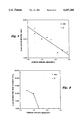
- FIG. 6 is a graph showing calibration curves for zirconium oxy-nitride thermistors obtained with different reactive gas flows in the sputtering atmosphere.
- the thin film resistors of this invention are especially characterized by virtue of the film being a metal oxy-nitride alloy and by their respective near-zero or large negative temperature coefficients of resistance. That is, the thin film resistors of this invention will be an alloy of both at least one electrically insulating oxide and an electrically conducting nitride of at least one metal which is capable of forming both a metal oxide and a metal nitride under reaction conditions.
- the metal oxide is, moreover, present in the thin film metal oxy-nitride alloys of this invention in an amount sufficient to provide for a desired temperature coefficient of resistance.
- the specific sensitivity is dependent only on the intrinsic properties of the film and independent of the film geometry.
- the sensitivity that the user observes in a thermometer is the rate of change of the resistance with temperature, dR/dT, which scales with the film geometry.
- the metal oxy-nitride films of this invention have a non-linear resistance/temperature characteristic, even on a log-log scale. As a result, thin films having varying amounts of metal oxide in the alloy are difficult to compare simply. However, an approximate comparison can be made by taking an average specific sensitivity between room temperature (approximately 295K) and liquid nitrogen temperature (77.35K).
- the term "average specific sensitivity" is intended to refer to a value which is expressed as ln(R 1 /R 2 )/ln(T 1 /T 2 ), where T 1 and T 2 represent the liquid nitrogen temperature and room temperature, respectively, and R 1 and R 2 represent the resistance in ohms ( ⁇ ) at temperatures T 1 and T 2 , respectively.
- the metals that may successfully be employed in the practice of this invention are those which are capable of forming both a metal oxide and a metal nitride under suitable conditions, for example, using a reactive gas comprised of an oxygen-containing gas and nitrogen.
- the metals may be, for example, titanium, tantalum, hafnium, zirconium, and niobium. These metals may be used alone, but could likewise be used in combinations of two or more so as to achieve the desired metal oxy-nitride film.
- the film resistors of this invention can be fabricated using any film deposition technique well known in this art.
- thin films may be fabricated using reactive sputtering of a pure metal target or a composite target of oxides, nitrides and/or metals, reactive evaporation, ion and ion assisted sputtering, ion plating, molecular beam epitaxy, chemical vapor deposition and deposition form organic precursors in the form of liquids.
- the thin film metal oxy-nitride alloys of this invention are fabricated by reactive sputtering.
- a metal target (which, as indicated previously, may be a combination of suitable metals) is sputtered onto a suitable substrate material in the presence of a reactive gas (which is preferably a mixture of both an oxygen-containing gas and a nitrogen gas in a suitable ratio) and an inert gas within a reaction chamber.
- a reactive gas which is preferably a mixture of both an oxygen-containing gas and a nitrogen gas in a suitable ratio
- an inert gas within a reaction chamber.
- a properly mixed target of the oxide and nitride ceramics could be sputtered in an atmosphere with sufficient background content of oxygen and nitrogen to prevent reduction of the sputtered material to the metal.
- the substrate material may be any suitable, readily available, electrically insulative material (e.g., alumina, sapphire, or the like) which (i) is chemically and physically compatible with the metal oxy-nitride film to be formed on at least one of the substrate surfaces, (ii) is stable at the deposition temperatures; and (iii) possesses a thermal expansion coefficient matching closely enough the thermal expansion coefficient of the film so that instability due to stress is not induced.
- the substrate should also preferably be of high purity. For example, when using alumina as a substrate in a reactive sputtering process, it is preferred to use 99.6% electronic grade alumina, mechanically polished to 0.3 microinch smoothness. If sapphire is employed as a substrate material, it is preferably a single crystal sapphire which has been chemically/mechanically polished to epitaxial quality.
- any inert gas may be employed in the reactive sputtering process to form the films of this invention.
- the inert gas will be argon for reasons of expense, but other inert gases such as neon, xenon and krypton could also be used.
- the selection of any particular inert gas is a balance between the economics of using a particular inert gas and the film properties that can be achieved as a result of its use.
- the reactive gas that is employed contains both an oxygen-containing gas and a nitrogen gas.
- the oxygen-containing gas is O 2 .
- Nitrous oxide or ozone could likewise be employed but for practical reasons are less desirable since they are toxic.
- the three necessary gases--i.e., the inert gas and the reactive gasses comprised of an oxygen-containing gas and a nitrogen gas-- may be admitted into the reaction chamber individually or, more preferably from the viewpoint of film consistency, premixed. That is, it is preferred to admit the argon separately into the reaction chamber but to premix the oxygen and nitrogen gases and then introduce the premixed oxygen and nitrogen gases into the reaction chamber.
- the inert gas and the reactive gasses comprised of an oxygen-containing gas and a nitrogen gas--may be admitted into the reaction chamber individually or, more preferably from the viewpoint of film consistency, premixed. That is, it is preferred to admit the argon separately into the reaction chamber but to premix the oxygen and nitrogen gases and then introduce the premixed oxygen and nitrogen gases into the reaction chamber.
- the reactive sputtering can either be accomplished using a substantially pure target (i.e., a target which is substantially free of reaction products) so as to increase the deposition rate, or a "poisoned" target (i.e., the target metal is allowed to react with the oxygen and nitrogen prior to being sputtered off the target).
- a substantially pure target i.e., a target which is substantially free of reaction products
- a "poisoned" target i.e., the target metal is allowed to react with the oxygen and nitrogen prior to being sputtered off the target.
- the substrate temperature range during reactive sputtering in which the negative temperature coefficient of resistance effect can be produced is from below room temperature up to about 700° C.
- the substrate temperature range is between 250° C. to 600° C. during reactive sputtering.
- the films have a tendency to peel from the substrate and exhibit a high degree of porosity and imperfection which lead to drift and high scatter in the thermometry properties.
- the magnetoresistances of the films change which may be used beneficially in some cases and may be detrimental in other cases, depending on the intended use of the sensor.
- the range of total gas pressure during deposition can be from 0.066 pascals to 6.6 pascals or higher, and more preferably between about 0.13 pascals to 1.33 pascals.
- the gas partial pressures do not necessarily need to be controlled directly, but their values are related to the gas flow versus magnetron power.
- the total pressure should be controlled to maintain a constant gas collision rate as the reactive gas portion is varied to obtain different TCR's.
- the mass flow of argon can be set at a value compatible with the pumping speed available and the desired total pressure. Magnetron power may then be chosen and fixed.
- the mass flow of the oxygen/nitrogen mixture can then be set at differing volume percentages of the argon flow to obtain the desired temperature coefficient of resistance.
- the pumping speed may then set according to a high sensitivity pressure sensor (e.g., a high sensitivity capacitance manometer) so as to maintain the desired total pressure.
- the ratio of the reactive gas flow (i.e., the volume flow of the oxygen/nitrogen gas mixture) to the argon gas flow is preferably between about 0.1 to 5, but more preferably is between 0.3 to 3.
- films from Nb, Ta, Zr and Hf can be produced with specific sensitivities between about -0.25 and -2.
- 5 vol. % O 2 in N 2 is preferable in order to produce the same range of specific sensitivities with substantially the same range of reactive gas to Ar ratios (volume basis). If the magnetron power is changed, the flow of the reactive gas must be changed in the same direction. If the O 2 to N 2 ratio is changed, the range of reactive gas to Ar ratios will change in the opposite direction in order to achieve the same specific sensitivity.
- ) for the metal oxy-nitride films of this invention is the smallest for the smallest percentage of reactive gas (i.e., the combined oxygen and nitrogen flow), and increases with the percentage increase of reactive gas until an insulating film is obtained.
- the films develop a "capacitive" aspect which slows their response to the application of electrical excitation to as much as several seconds, which limits the useful films to a reactive element content which produces an absolute value of the specific sensitivity of less than about 3.0 in the region of room temperature, depending on the requirements of use.
- nearly stoichiometric nitride films of the metals described previously can be made with the reactive sputtering method described above using pure nitrogen flow in addition to the argon, and these films exhibit a positive temperature coefficient.
- the flow rate of the reactive gas during sputter deposition affects the structure of the metal oxy-nitride films, which in turn affects the electrical properties.
- Films formed with low flow rates of reactive gas consist mostly of ZrN, which has a cubic structure.
- SEM and TEM, respectively scanning and transmission electron microscope (SEM and TEM, respectively) examination of film morphology reveals a completely dense microstructure.
- the films typically show a preferred (111) orientation of crystal planes in the plane of the substrate.
- the mean spacing, d, between (111) planes in the film increases, indicating enlargement or distortion of the lattice by incorporation of additional oxygen in the crystal lattice.
- the relationship between the lattice spacing d and the specific sensitivities (which vary directly with the reactive gas flow rates) of zirconium oxy-nitride films according to this invention is shown in FIG. 1.
- the oxygen present in the film is incorporated into the lattice of the ZrN until a specific sensitivity of about -0.6 is reached. At this point, the formation of a separate phase, ZrO 2 , becomes evident as is seen from FIG. 2.
- the ZrO 2 is electrically insulating and tetragonal in structure, and its presence continues to distort the ZrN lattice (see FIG. 1), increasing the absolute value of the specific sensitivity.
- the diffraction peak is broader than that for stoichiometric ZrN for all negative specific sensitivities, but never as broad as would be expected for amorphous material, thereby indicating a distorted periodic lattice.
- the specific sensitivity increases with the width in the same manner as with the lattice spacing.
- the insulating metal oxide (e.g., ZrO 2 ) phase does not become the major, or host, phase, even at specific sensitivities beyond the useful range (about
- conventional cermets having the same type of resistivity versus temperature characteristics must have the insulating phase be the major phase, or nearly so (greater than 40% by volume), to have an appreciable specific sensitivity.
- the metal oxy-nitride films of this invention exhibit an average specific sensitivity of between about +0.5 to about -5.0.
- film resistors useful for fabricating thermistors e.g., films having an average specific sensitivity between about -0.25 to about -2.0
- circuit resistors e.g., films having an average specific sensitivity between about ⁇ 0.5, and more preferably between about ⁇ 0.03.
- films with an average specific sensitivity between about -0.25 to about -0.4 can be used in thermometry from above room temperature to as low as a few tens of millikelvins.
- films with an average specific sensitivity between about -0.4 to about -1.0 can be used in thermometry from well above room temperature to below 1 K.
- Films with an average specific sensitivity from about -1.0 to about -1.5 are useful from about 4K to above room temperature
- films with an average specific sensitivity from about -1.5 to -2 are useful from temperatures about 10K to 20K to above room temperature.
- Space charge effects begin to be a consideration above about an absolute value of the average specific sensitivity of 2. The exact temperature range of usefulness depends upon the geometry (hence the total resistance) and the measuring instrument capability.
- platinum resistance thermometers have a specific sensitivity of about +1
- conventional bulk thermistors have specific sensitivities from about -3 to -6.
- the stoichiometric nitrides of this group of metals, TiN, NbN, TaN, ZrN and HfN are metals that exhibit a positive temperature coefficient.
- FIG. 4 shows that films can easily be formed by this method with an average specific sensitivity of about ⁇ 0.03.
- the temperature coefficient is equivalent to about ⁇ 100 parts per million (ppm) per °C., which is quite adequate for room temperature electronic circuit resistors.
- ppm parts per million
- this low TCR is maintained over a very wide range of temperatures ( ⁇ 200° C.), in contrast to most conventional thick film electronics resistors, which frequently increase to 400 ppm at ⁇ 50° C. from 100 ppm at 25° C.
- the metal oxy-nitride films according to this invention may be fabricated into thin film thermistors of desired geometry employing conventional fabrication technology.
- the metal oxy-nitride films of this invention may be fabricated into thermistors and resistors having the geometry as described in commonly owned and copending U.S. application Ser. No. 08/024,273 filed even date herewith in the name of Philip R. Swinehart (Atty. Dkt. No. 340-21), the entire content of which is expressly incorporated hereinto by reference.
- the thermistors and resistors will include at least one pair of electrical contacts in electrical communication with the film so as to electrically connect the film to external circuitry.
- the electrical contacts employed with the metal oxy-nitride films of this invention must be stable. That is, if the contact resistances are not sufficiently stable, the instability will be read by sensing circuitry as a temperature change or drift out of resistance tolerance (since the contact resistances will add in series with the desired resistance of the active film material).
- stable electrical contacts employed with the metal oxy-nitride films of this invention are selected so as to substantially avoid exchange of oxygen at the electrode/film interface. That is, since oxygen is a very reactive element, and since the metal oxy-nitride films according to this invention contain oxides, the choice of improper electrodes could cause a chemical reaction with the resulting exchange of oxygen between the electrodes and the active body.
- the oxide loss or gain of oxygen in the active body film will affect the resistance, and further, if the electrode material forms an insulating oxide, a large series resistance error will occur.
- Reactive metals which form insulating oxides such as Ti, Zr, Ta and Hf, must therefore be avoided as electrical contact materials.
- the materials from which stable electrical contacts can be fabricated for use with the metal oxy-nitride films according to this invention include low oxidation potential metals such as Pt, Rh, Pd, W, Mo, Ru, Re, Os and Ir, as well as rutile crystal structure oxides of such metals, i.e., WO 2 , ReO 2 , RuO 2 , RhO 2 , MoO 2 , IrO 2 , PtO 2 and OsO 1 .
- Electrical contacts can also be formed of relatively simple sodium chloride structure oxides, such as TiO, NbO, SnO 2 , In 2 O 3 , WO 3 and MoO 3 can be employed if self-doped by non-stoichiometry. Oxides having a perovskite crystal structure, such as ReO 3 , may also be employed. Electrical contacts formed of the materials described above will provide enhanced stability at substantially higher temperature than room temperature and under thermal cycling stress.
- a 2.5 cm diameter permanent magnet magnetron was used in a cryopumped vacuum system capable of a base pressure in the 7 ⁇ 10 -6 pascal range.
- the substrates were mechanically polished 99.6% alumina or epitaxially polished R-cut sapphire placed at 7 to 10 cm from the magnetron.
- the substrates were cleaned with an argon ion beam and heated to about 300° C.
- the magnetron power was fixed at 150 Watts dc and the total pressure was 0.266 pascal to limit the number of collisions for sputtered atoms before they reached the substrate.
- An ultra-high purity grade, 1.01 vol. % O 2 in N 2 was used for Ta, Zr, Hf, and Nb.
- the flow rate of Ar was chosen to be in the mid-range of flow and throttle control (33 sccm) so that no other parameters would have to be changed as the reactive gas flow was changed.
- the following procedures were followed: (1) the gas flows were established; (2) the pump throttle valve was set so that the total pressure was 0.266 pascal, (3) the target was conditioned by presputtering with the shutter closed for several minutes; and then (4) film formation was accomplished by sputtering for a sufficiently long time to obtain films in the 300 nm thickness range. Between each deposition, the thickness was measured on a stylus profilometer and the average specific sensitivity was measured with a four point probe between room temperature and liquid nitrogen temperature. The obtained data were plotted and appear in accompanying FIG. 4.
- Example 1 In order to evaluate the effect of a change in the oxygen to nitrogen ratio, Example 1 was repeated for titanium, except that 30 vol % O 2 in N 2 was used which was further mixed with pure N 2 in a chamber connected to the sputtering system in order to obtain mixtures corresponding to 5 vol. %, 10 vol. % and 30 vol. % O 2 in N 2 .
- Titanium oxy-nitride films having a wide range of sensitivities, from zero to an absolute value of the average specific sensitivity greater than 2 were fabricated as shown by the data appearing in accompanying FIG. 5 (which also includes the data for titanium oxy-nitride films produced using 1.01 vol. % O 2 in N 2 obtained according to Example 1 above).
- thermistors Six zirconium oxy-nitride film samples were fabricated into finished thermistors identified as R1 through R6, respectively, having a geometry as disclosed in the Examples of the above-identified copending U.S. patent application Ser. No. 08,024,273 (Atty. Dkt. 340-22).
- the thermistors R1-R6 were each wire bonded (gold thermosonic ball bonded) and sealed into hermetic ceramic packages.
- Experimental calibration data for each of the thermistors was obtained by a calibration system using secondary standard thermometers and resistance standards traceable to the National Institute of Standards and Technology (NIST). The obtained calibration data appear in FIG. 6.
- FIGS. 4-6 demonstrate several significant attributes of the metal oxy-nitride films according to this invention.
- the effect of changing the oxygen to nitrogen ratio can be seen in the data of FIG. 4 relating to the titanium oxy-nitride films. That is, comparing the two curves for titanium in FIG. 5--i.e., the curves representing substantially 1 vol. % O 2 in N 2 and 5 vol. % O 2 in N 2 , it can be seen that the former reactive gas ratio has little effect, whereas the latter produces a response to increasing reactive gas flow similar to those for Ta, Zr, Hf and Nb metals at the 1 vol. % O 2 level.
- FIG. 5- the curves representing substantially 1 vol. % O 2 in N 2 and 5 vol. % O 2 in N 2
Abstract
Description
Claims (27)
Priority Applications (1)
| Application Number | Priority Date | Filing Date | Title |
|---|---|---|---|
| US08/025,411 US5367285A (en) | 1993-02-26 | 1993-02-26 | Metal oxy-nitride resistance films and methods of making the same |
Applications Claiming Priority (1)
| Application Number | Priority Date | Filing Date | Title |
|---|---|---|---|
| US08/025,411 US5367285A (en) | 1993-02-26 | 1993-02-26 | Metal oxy-nitride resistance films and methods of making the same |
Publications (1)
| Publication Number | Publication Date |
|---|---|
| US5367285A true US5367285A (en) | 1994-11-22 |
Family
ID=21825901
Family Applications (1)
| Application Number | Title | Priority Date | Filing Date |
|---|---|---|---|
| US08/025,411 Expired - Lifetime US5367285A (en) | 1993-02-26 | 1993-02-26 | Metal oxy-nitride resistance films and methods of making the same |
Country Status (1)
| Country | Link |
|---|---|
| US (1) | US5367285A (en) |
Cited By (22)
| Publication number | Priority date | Publication date | Assignee | Title |
|---|---|---|---|---|
| US5585776A (en) * | 1993-11-09 | 1996-12-17 | Research Foundation Of The State University Of Ny | Thin film resistors comprising ruthenium oxide |
| US5668524A (en) * | 1994-02-09 | 1997-09-16 | Kyocera Corporation | Ceramic resistor and electrostatic chuck having an aluminum nitride crystal phase |
| US5948216A (en) * | 1996-05-17 | 1999-09-07 | Lucent Technologies Inc. | Method for making thin film tantalum oxide layers with enhanced dielectric properties and capacitors employing such layers |
| WO2001010552A1 (en) | 1999-08-05 | 2001-02-15 | Kabushiki Kaisha Toyota Chuo Kenkyusho | Photocatalytic material, photocatalytic article and method for their preparation |
| US6265746B1 (en) * | 1998-05-28 | 2001-07-24 | Altera Corporation | Highly resistive interconnects |
| US6312567B1 (en) | 1996-03-21 | 2001-11-06 | Tong Yang Cement Corporation | Method of forming a (200)-oriented platinum layer |
| US6413385B1 (en) * | 1997-05-19 | 2002-07-02 | Nec Corporation | Thin-film temperature-sensitive resistor material and production process thereof |
| US6480093B1 (en) | 2000-01-26 | 2002-11-12 | Yang-Yuan Chen | Composite film resistors and method of making the same |
| US6576967B1 (en) | 2000-09-18 | 2003-06-10 | Motorola, Inc. | Semiconductor structure and process for forming a metal oxy-nitride dielectric layer |
| US6576482B1 (en) | 2002-05-07 | 2003-06-10 | Texas Instruments Incorporated | One step deposition process for the top electrode and hardmask in a ferroelectric memory cell |
| US6799838B2 (en) * | 1998-08-31 | 2004-10-05 | Canon Kabushiki Kaisha | Liquid discharge head liquid discharge method and liquid discharge apparatus |
| US20070126548A1 (en) * | 2005-12-07 | 2007-06-07 | Knobloch Aaron J | Thermistor having doped and undoped layers of material |
| US20080036955A1 (en) * | 2006-06-21 | 2008-02-14 | Taek Hee Kim | Method of Forming Metal Thin Film and Metal Wiring Pattern and Method of Manufacturing Display Panel |
| US20090148595A1 (en) * | 2006-03-03 | 2009-06-11 | Yoshinori Nagamine | Method of Manufacturing Magnetoresistance Effect Element and Apparatus for Manufacturing the Same |
| WO2009129930A1 (en) * | 2008-04-24 | 2009-10-29 | Hochschule Für Technik Und Wirtschaft Des Saarlandes | Film resistor with a constant temperature coefficient and production of a film resistor of this type |
| US20100213574A1 (en) * | 2004-08-31 | 2010-08-26 | Micron Technology, Inc. | High dielectric constant transition metal oxide materials |
| US20120274318A1 (en) * | 2011-04-27 | 2012-11-01 | Applied Materials, Inc. | Methods and apparatus to determine parameters in metal-containing films |
| TWI401745B (en) * | 2007-07-13 | 2013-07-11 | Hitachi Ltd | Semiconductor device and manufacturing method thereof |
| US20150023394A1 (en) * | 2012-02-28 | 2015-01-22 | Mitsubishi Materials Corporation | Metal nitride material for thermistor, method for producing same, and film thermistor sensor |
| US20200166415A1 (en) * | 2017-05-09 | 2020-05-28 | Flosfia Inc. | Thermistor film and method of depositing the same |
| KR20210137346A (en) | 2020-05-09 | 2021-11-17 | 제이에이취엔지니어링주식회사 | The manufacturing system of the cryogenic sensor for recycling and the system using it |
| US11532410B2 (en) * | 2017-12-25 | 2022-12-20 | Mitsubishi Materials Corporation | Thermistor, method for manufacturing same, and thermistor sensor |
Citations (29)
| Publication number | Priority date | Publication date | Assignee | Title |
|---|---|---|---|---|
| US3591479A (en) * | 1969-05-08 | 1971-07-06 | Ibm | Sputtering process for preparing stable thin film resistors |
| US3664943A (en) * | 1969-06-25 | 1972-05-23 | Oki Electric Ind Co Ltd | Method of producing tantalum nitride film resistors |
| US3763026A (en) * | 1969-12-22 | 1973-10-02 | Gen Electric | Method of making resistor thin films by reactive sputtering from a composite source |
| US3803057A (en) * | 1971-03-11 | 1974-04-09 | Matsushita Electric Ind Co Ltd | Resistive materials and method of making such materials |
| US4016061A (en) * | 1971-03-11 | 1977-04-05 | Matsushita Electric Industrial Co., Ltd. | Method of making resistive films |
| US4025892A (en) * | 1974-05-27 | 1977-05-24 | U.S. Philips Corporation | Probe for detecting gaseous polar molecules such as water vapor |
| US4100524A (en) * | 1976-05-06 | 1978-07-11 | Gould Inc. | Electrical transducer and method of making |
| US4104607A (en) * | 1977-03-14 | 1978-08-01 | The United States Of America As Represented By The Secretary Of The Navy | Zero temperature coefficient of resistance bi-film resistor |
| US4104421A (en) * | 1974-11-29 | 1978-08-01 | Sprague Electric Company | Method of making a glass containing resistor having a sub-micron metal film termination |
| US4183746A (en) * | 1975-12-24 | 1980-01-15 | Johnson, Matthey & Co., Limited | Cermets |
| US4280114A (en) * | 1979-09-24 | 1981-07-21 | University Of Pittsburgh | Discontinuous metal and cermet film resistors and strain gauges |
| US4359372A (en) * | 1979-10-11 | 1982-11-16 | Matsushita Electric Industrial Company, Limited | Method for making a carbide thin film thermistor |
| US4398169A (en) * | 1980-06-23 | 1983-08-09 | Masaki Hayashi | Resistance thermometer element |
| US4454495A (en) * | 1982-08-31 | 1984-06-12 | The United States Of America As Represented By The United States Department Of Energy | Layered ultra-thin coherent structures used as electrical resistors having low temperature coefficient of resistivity |
| US4521287A (en) * | 1984-06-28 | 1985-06-04 | General Motors Corporation | High rate sputtering of exhaust oxygen sensor electrode |
| US4526785A (en) * | 1983-10-21 | 1985-07-02 | Corning Glass Works | Metal patterns on photosensitive glasses |
| US4609903A (en) * | 1983-10-20 | 1986-09-02 | Fujitsu Limited | Thin film resistor for an integrated circuit semiconductor device |
| JPS62269102A (en) * | 1986-05-16 | 1987-11-21 | Nisshin Steel Co Ltd | Infrared ray reflective material |
| JPS63224201A (en) * | 1987-03-12 | 1988-09-19 | 大阪府 | Temperature measuring resistor for thermometer not sensitive to magnetic field under cryogenic conditions |
| US4774151A (en) * | 1986-05-23 | 1988-09-27 | International Business Machines Corporation | Low contact electrical resistant composition, substrates coated therewith, and process for preparing such |
| US4849079A (en) * | 1986-05-23 | 1989-07-18 | International Business Machines Corp. | Process for preparing low electrical contact resistance composition |
| US4888246A (en) * | 1985-05-23 | 1989-12-19 | Matsushita Electric Industrial Co., Ltd. | Dielectric thin film, and method for making the thin film |
| US4895765A (en) * | 1985-09-30 | 1990-01-23 | Union Carbide Corporation | Titanium nitride and zirconium nitride coating compositions, coated articles and methods of manufacture |
| US4906968A (en) * | 1988-10-04 | 1990-03-06 | Cornell Research Foundation, Inc. | Percolating cermet thin film thermistor |
| US4997538A (en) * | 1988-06-24 | 1991-03-05 | Asulab S.A. | Process for depositing a black-colored coating on a substrate and a black-colored coating obtained using this process |
| US5108571A (en) * | 1989-08-16 | 1992-04-28 | Leybold Aktiengesellschaft | Process for coating a dielectric substrate with copper |
| US5156725A (en) * | 1991-10-17 | 1992-10-20 | The Dow Chemical Company | Method for producing metal carbide or carbonitride coating on ceramic substrate |
| US5158933A (en) * | 1990-11-15 | 1992-10-27 | Holtz Ronald L | Phase separated composite materials |
| US5171412A (en) * | 1991-08-23 | 1992-12-15 | Applied Materials, Inc. | Material deposition method for integrated circuit manufacturing |
-
1993
- 1993-02-26 US US08/025,411 patent/US5367285A/en not_active Expired - Lifetime
Patent Citations (30)
| Publication number | Priority date | Publication date | Assignee | Title |
|---|---|---|---|---|
| US3591479A (en) * | 1969-05-08 | 1971-07-06 | Ibm | Sputtering process for preparing stable thin film resistors |
| US3664943A (en) * | 1969-06-25 | 1972-05-23 | Oki Electric Ind Co Ltd | Method of producing tantalum nitride film resistors |
| US3763026A (en) * | 1969-12-22 | 1973-10-02 | Gen Electric | Method of making resistor thin films by reactive sputtering from a composite source |
| US3803057A (en) * | 1971-03-11 | 1974-04-09 | Matsushita Electric Ind Co Ltd | Resistive materials and method of making such materials |
| US4016061A (en) * | 1971-03-11 | 1977-04-05 | Matsushita Electric Industrial Co., Ltd. | Method of making resistive films |
| US4025892A (en) * | 1974-05-27 | 1977-05-24 | U.S. Philips Corporation | Probe for detecting gaseous polar molecules such as water vapor |
| US4104421A (en) * | 1974-11-29 | 1978-08-01 | Sprague Electric Company | Method of making a glass containing resistor having a sub-micron metal film termination |
| US4183746A (en) * | 1975-12-24 | 1980-01-15 | Johnson, Matthey & Co., Limited | Cermets |
| US4100524A (en) * | 1976-05-06 | 1978-07-11 | Gould Inc. | Electrical transducer and method of making |
| US4104607A (en) * | 1977-03-14 | 1978-08-01 | The United States Of America As Represented By The Secretary Of The Navy | Zero temperature coefficient of resistance bi-film resistor |
| US4280114A (en) * | 1979-09-24 | 1981-07-21 | University Of Pittsburgh | Discontinuous metal and cermet film resistors and strain gauges |
| US4359372A (en) * | 1979-10-11 | 1982-11-16 | Matsushita Electric Industrial Company, Limited | Method for making a carbide thin film thermistor |
| US4398169A (en) * | 1980-06-23 | 1983-08-09 | Masaki Hayashi | Resistance thermometer element |
| US4454495A (en) * | 1982-08-31 | 1984-06-12 | The United States Of America As Represented By The United States Department Of Energy | Layered ultra-thin coherent structures used as electrical resistors having low temperature coefficient of resistivity |
| US4609903A (en) * | 1983-10-20 | 1986-09-02 | Fujitsu Limited | Thin film resistor for an integrated circuit semiconductor device |
| US4526785A (en) * | 1983-10-21 | 1985-07-02 | Corning Glass Works | Metal patterns on photosensitive glasses |
| US4521287A (en) * | 1984-06-28 | 1985-06-04 | General Motors Corporation | High rate sputtering of exhaust oxygen sensor electrode |
| US4888246A (en) * | 1985-05-23 | 1989-12-19 | Matsushita Electric Industrial Co., Ltd. | Dielectric thin film, and method for making the thin film |
| US4895765A (en) * | 1985-09-30 | 1990-01-23 | Union Carbide Corporation | Titanium nitride and zirconium nitride coating compositions, coated articles and methods of manufacture |
| JPS62269102A (en) * | 1986-05-16 | 1987-11-21 | Nisshin Steel Co Ltd | Infrared ray reflective material |
| US4774151A (en) * | 1986-05-23 | 1988-09-27 | International Business Machines Corporation | Low contact electrical resistant composition, substrates coated therewith, and process for preparing such |
| US4849079A (en) * | 1986-05-23 | 1989-07-18 | International Business Machines Corp. | Process for preparing low electrical contact resistance composition |
| JPS63224201A (en) * | 1987-03-12 | 1988-09-19 | 大阪府 | Temperature measuring resistor for thermometer not sensitive to magnetic field under cryogenic conditions |
| US5030522A (en) * | 1988-06-24 | 1991-07-09 | Asulab S.A. | Black-colored coating deposited on a substrate |
| US4997538A (en) * | 1988-06-24 | 1991-03-05 | Asulab S.A. | Process for depositing a black-colored coating on a substrate and a black-colored coating obtained using this process |
| US4906968A (en) * | 1988-10-04 | 1990-03-06 | Cornell Research Foundation, Inc. | Percolating cermet thin film thermistor |
| US5108571A (en) * | 1989-08-16 | 1992-04-28 | Leybold Aktiengesellschaft | Process for coating a dielectric substrate with copper |
| US5158933A (en) * | 1990-11-15 | 1992-10-27 | Holtz Ronald L | Phase separated composite materials |
| US5171412A (en) * | 1991-08-23 | 1992-12-15 | Applied Materials, Inc. | Material deposition method for integrated circuit manufacturing |
| US5156725A (en) * | 1991-10-17 | 1992-10-20 | The Dow Chemical Company | Method for producing metal carbide or carbonitride coating on ceramic substrate |
Non-Patent Citations (16)
| Title |
|---|
| Gershenfeld et al, "Percolating Cermet Thin-Film Thermistors Between 50 mK-300K and 0-20 T", J. Appl. Phys. 64(9), 1 Nov. 1988. |
| Gershenfeld et al, Percolating Cermet Thin Film Thermistors Between 50 mK 300K and 0 20 T , J. Appl. Phys. 64(9), 1 Nov. 1988. * |
| Holmes et al, "Resolution and Accuracy of Cryogenic Temperature Measurements", Temperature: Its Measurement and Control in Science and Industry, vol. 6, part 2, American Inst. Phys., pp. 1225-1230 (1992). |
| Holmes et al, Resolution and Accuracy of Cryogenic Temperature Measurements , Temperature: Its Measurement and Control in Science and Industry, vol. 6, part 2, American Inst. Phys., pp. 1225 1230 (1992). * |
| Luthier et al, "Magnetron Sputtered TiAlON Composite Thin Films. I. Structure and Morphology", J. Vac. Sci. Technol. A 9(1), pp. 102-109 Jan./Feb. 1991. |
| Luthier et al, "Magnetron Sputtered TiAlON Composite Thin Films. II. Optical and Electrical Properties", J. Vac. Sci. Technol. A 9(1), pp. 110-115 Jan./Feb. 1991. |
| Luthier et al, Magnetron Sputtered TiAlON Composite Thin Films. I. Structure and Morphology , J. Vac. Sci. Technol. A 9(1), pp. 102 109 Jan./Feb. 1991. * |
| Luthier et al, Magnetron Sputtered TiAlON Composite Thin Films. II. Optical and Electrical Properties , J. Vac. Sci. Technol. A 9(1), pp. 110 115 Jan./Feb. 1991. * |
| Meng et al, "Electrical Transport and Optical Properties of Zirconium Nitride/Aluminum Nitride Multilayers", J. Appl. Phys. 69(2), 15 Jan. 1991. |
| Meng et al, Electrical Transport and Optical Properties of Zirconium Nitride/Aluminum Nitride Multilayers , J. Appl. Phys. 69(2), 15 Jan. 1991. * |
| Yotsuya et al, "New Type Cryogenic Thermometer Using Sputtered Zr-N Films", Appl. Phys. Lett..51(4), 27 Jul. 1987. |
| Yotsuya et al, "Thin Film Cryogenic Thermometer with Thermometric Calibration Point", Proceedings of the 5th Sensor Symposium, pp. 9-14 (1985). |
| Yotsuya et al, "Zr-N Thin Film Thermometer for Cryogenic Temperature", pp. 154-155 (Jan. 19, 1982). |
| Yotsuya et al, New Type Cryogenic Thermometer Using Sputtered Zr N Films , Appl. Phys. Lett.. 51(4), 27 Jul. 1987. * |
| Yotsuya et al, Thin Film Cryogenic Thermometer with Thermometric Calibration Point , Proceedings of the 5th Sensor Symposium, pp. 9 14 (1985). * |
| Yotsuya et al, Zr N Thin Film Thermometer for Cryogenic Temperature , pp. 154 155 (Jan. 19, 1982). * |
Cited By (34)
| Publication number | Priority date | Publication date | Assignee | Title |
|---|---|---|---|---|
| US5585776A (en) * | 1993-11-09 | 1996-12-17 | Research Foundation Of The State University Of Ny | Thin film resistors comprising ruthenium oxide |
| US5777543A (en) * | 1994-01-09 | 1998-07-07 | Kyocera Corporation | Ceramic resistor and electrostatic chuck having an aluminum nitride crystal phase |
| US5668524A (en) * | 1994-02-09 | 1997-09-16 | Kyocera Corporation | Ceramic resistor and electrostatic chuck having an aluminum nitride crystal phase |
| US6312567B1 (en) | 1996-03-21 | 2001-11-06 | Tong Yang Cement Corporation | Method of forming a (200)-oriented platinum layer |
| US5948216A (en) * | 1996-05-17 | 1999-09-07 | Lucent Technologies Inc. | Method for making thin film tantalum oxide layers with enhanced dielectric properties and capacitors employing such layers |
| US6413385B1 (en) * | 1997-05-19 | 2002-07-02 | Nec Corporation | Thin-film temperature-sensitive resistor material and production process thereof |
| US6265746B1 (en) * | 1998-05-28 | 2001-07-24 | Altera Corporation | Highly resistive interconnects |
| US6799838B2 (en) * | 1998-08-31 | 2004-10-05 | Canon Kabushiki Kaisha | Liquid discharge head liquid discharge method and liquid discharge apparatus |
| WO2001010552A1 (en) | 1999-08-05 | 2001-02-15 | Kabushiki Kaisha Toyota Chuo Kenkyusho | Photocatalytic material, photocatalytic article and method for their preparation |
| EP1205244A1 (en) * | 1999-08-05 | 2002-05-15 | Kabushiki Kaisha Toyota Chuo Kenkyusho | Photocatalytic material, photocatalytic article and method for their preparation |
| EP1205244A4 (en) * | 1999-08-05 | 2005-01-19 | Toyoda Chuo Kenkyusho Kk | Photocatalytic material, photocatalytic article and method for their preparation |
| US6480093B1 (en) | 2000-01-26 | 2002-11-12 | Yang-Yuan Chen | Composite film resistors and method of making the same |
| US6576967B1 (en) | 2000-09-18 | 2003-06-10 | Motorola, Inc. | Semiconductor structure and process for forming a metal oxy-nitride dielectric layer |
| US6743668B2 (en) | 2000-09-18 | 2004-06-01 | Motorola, Inc. | Process for forming a metal oxy-nitride dielectric layer by varying the flow rate of nitrogen into the chamber |
| US6576482B1 (en) | 2002-05-07 | 2003-06-10 | Texas Instruments Incorporated | One step deposition process for the top electrode and hardmask in a ferroelectric memory cell |
| US8791519B2 (en) * | 2004-08-31 | 2014-07-29 | Micron Technology, Inc. | High dielectric constant transition metal oxide materials |
| US20100213574A1 (en) * | 2004-08-31 | 2010-08-26 | Micron Technology, Inc. | High dielectric constant transition metal oxide materials |
| US20070126548A1 (en) * | 2005-12-07 | 2007-06-07 | Knobloch Aaron J | Thermistor having doped and undoped layers of material |
| US7880580B2 (en) * | 2005-12-07 | 2011-02-01 | General Electric Company | Thermistor having doped and undoped layers of material |
| US20090148595A1 (en) * | 2006-03-03 | 2009-06-11 | Yoshinori Nagamine | Method of Manufacturing Magnetoresistance Effect Element and Apparatus for Manufacturing the Same |
| US10629804B2 (en) * | 2006-03-03 | 2020-04-21 | Canon Anelva Corporation | Method of manufacturing magnetoresistive device |
| US20080036955A1 (en) * | 2006-06-21 | 2008-02-14 | Taek Hee Kim | Method of Forming Metal Thin Film and Metal Wiring Pattern and Method of Manufacturing Display Panel |
| US7662675B2 (en) * | 2006-06-21 | 2010-02-16 | Samsung Electronics Co., Ltd. | Method of forming metal thin film and metal wiring pattern and method of manufacturing display panel |
| TWI401745B (en) * | 2007-07-13 | 2013-07-11 | Hitachi Ltd | Semiconductor device and manufacturing method thereof |
| US8198978B2 (en) | 2008-04-24 | 2012-06-12 | Hochschule fur Technik und Wirtschaft des Sarlandes | Film resistor with a constant temperature coefficient and production of a film resistor of this type |
| WO2009129930A1 (en) * | 2008-04-24 | 2009-10-29 | Hochschule Für Technik Und Wirtschaft Des Saarlandes | Film resistor with a constant temperature coefficient and production of a film resistor of this type |
| US20120274318A1 (en) * | 2011-04-27 | 2012-11-01 | Applied Materials, Inc. | Methods and apparatus to determine parameters in metal-containing films |
| US9880233B2 (en) * | 2011-04-27 | 2018-01-30 | Applied Materials, Inc. | Methods and apparatus to determine parameters in metal-containing films |
| US20150023394A1 (en) * | 2012-02-28 | 2015-01-22 | Mitsubishi Materials Corporation | Metal nitride material for thermistor, method for producing same, and film thermistor sensor |
| US9852829B2 (en) * | 2012-02-28 | 2017-12-26 | Mitsubishi Materials Corporation | Metal nitride material for thermistor, method for producing same, and film thermistor sensor |
| US20200166415A1 (en) * | 2017-05-09 | 2020-05-28 | Flosfia Inc. | Thermistor film and method of depositing the same |
| US10989609B2 (en) * | 2017-05-09 | 2021-04-27 | Flosfia Inc. | Thermistor film and method of depositing the same |
| US11532410B2 (en) * | 2017-12-25 | 2022-12-20 | Mitsubishi Materials Corporation | Thermistor, method for manufacturing same, and thermistor sensor |
| KR20210137346A (en) | 2020-05-09 | 2021-11-17 | 제이에이취엔지니어링주식회사 | The manufacturing system of the cryogenic sensor for recycling and the system using it |
Similar Documents
| Publication | Publication Date | Title |
|---|---|---|
| US5367285A (en) | Metal oxy-nitride resistance films and methods of making the same | |
| JP4436064B2 (en) | Thermistor material and manufacturing method thereof | |
| JPS5945201B2 (en) | Electrical resistance film and its manufacturing method | |
| US4276535A (en) | Thermistor | |
| US5733669A (en) | Resistive component comprising a CRSI resistive film | |
| JPH06158272A (en) | Resistance film and production thereof | |
| Mooij et al. | Structural and electrical properties of sputtered CrNi films | |
| US5585776A (en) | Thin film resistors comprising ruthenium oxide | |
| US5281845A (en) | PTCR device | |
| EP1058276B1 (en) | Thin film thermistor element and method for the fabrication of thin film thermistor element | |
| US5001454A (en) | Thin film resistor for strain gauge | |
| WO1986004989A1 (en) | Gas sensor element of tin oxide film | |
| JPS634321B2 (en) | ||
| Thomas et al. | Structural, electrical and optical properties of sol–gel processed lead titanate thin films | |
| JPH11271145A (en) | Detection film for use in bolometer and its formation, and bolometer element | |
| US6480093B1 (en) | Composite film resistors and method of making the same | |
| JPH0666162B2 (en) | Thin film resistor for strain gauge | |
| JP4858912B2 (en) | Method for producing SrRuO3 film and obtained film | |
| EP1504460A1 (en) | Improved electrode for thin film capacitor devices | |
| EP2871649B1 (en) | Dielectric composition, dielectric film, and electronic component | |
| Nagai et al. | SiC thin-film thermistor | |
| JP4277380B2 (en) | Thin film thermistor element | |
| JPS60208803A (en) | Method of producing thin film thermistor | |
| JPH0276201A (en) | Thin film resistor for strain gauge | |
| JP2001110606A (en) | Resistance bulb for thermometer unaffected by magnetic field under very low temperature |
Legal Events
| Date | Code | Title | Description |
|---|---|---|---|
| AS | Assignment |
Owner name: LAKE SHORE CRYOTRONICS, INC., OHIO Free format text: ASSIGNMENT OF ASSIGNORS INTEREST;ASSIGNORS:SWINEHART, PHILIP R.;COURTS, S. SCOTT;HOLMES, S. SCOTT;REEL/FRAME:006552/0584 Effective date: 19930309 |
|
| STCF | Information on status: patent grant |
Free format text: PATENTED CASE |
|
| REMI | Maintenance fee reminder mailed | ||
| FEPP | Fee payment procedure |
Free format text: PETITION RELATED TO MAINTENANCE FEES FILED (ORIGINAL EVENT CODE: PMFP); ENTITY STATUS OF PATENT OWNER: LARGE ENTITY |
|
| FPAY | Fee payment |
Year of fee payment: 4 |
|
| FP | Lapsed due to failure to pay maintenance fee |
Effective date: 19981122 |
|
| FEPP | Fee payment procedure |
Free format text: PETITION RELATED TO MAINTENANCE FEES GRANTED (ORIGINAL EVENT CODE: PMFG); ENTITY STATUS OF PATENT OWNER: LARGE ENTITY Free format text: PAT HOLDER NO LONGER CLAIMS SMALL ENTITY STATUS, ENTITY STATUS SET TO UNDISCOUNTED (ORIGINAL EVENT CODE: STOL); ENTITY STATUS OF PATENT OWNER: LARGE ENTITY |
|
| FPAY | Fee payment |
Year of fee payment: 8 |
|
| FEPP | Fee payment procedure |
Free format text: ENTITY STATUS SET TO UNDISCOUNTED (ORIGINAL EVENT CODE: BIG.); ENTITY STATUS OF PATENT OWNER: LARGE ENTITY |
|
| SULP | Surcharge for late payment | ||
| REMI | Maintenance fee reminder mailed | ||
| PRDP | Patent reinstated due to the acceptance of a late maintenance fee |
Effective date: 20020527 |
|
| FPAY | Fee payment |
Year of fee payment: 12 |