US5374590A - Fabrication and laser deletion of microfuses - Google Patents
Fabrication and laser deletion of microfuses Download PDFInfo
- Publication number
- US5374590A US5374590A US08/053,282 US5328293A US5374590A US 5374590 A US5374590 A US 5374590A US 5328293 A US5328293 A US 5328293A US 5374590 A US5374590 A US 5374590A
- Authority
- US
- United States
- Prior art keywords
- microfuse
- diameter
- equals
- fuse link
- accuracy
- Prior art date
- Legal status (The legal status is an assumption and is not a legal conclusion. Google has not performed a legal analysis and makes no representation as to the accuracy of the status listed.)
- Expired - Fee Related
Links
Images

Classifications
-
- H—ELECTRICITY
- H01—ELECTRIC ELEMENTS
- H01L—SEMICONDUCTOR DEVICES NOT COVERED BY CLASS H10
- H01L23/00—Details of semiconductor or other solid state devices
- H01L23/52—Arrangements for conducting electric current within the device in operation from one component to another, i.e. interconnections, e.g. wires, lead frames
- H01L23/522—Arrangements for conducting electric current within the device in operation from one component to another, i.e. interconnections, e.g. wires, lead frames including external interconnections consisting of a multilayer structure of conductive and insulating layers inseparably formed on the semiconductor body
- H01L23/525—Arrangements for conducting electric current within the device in operation from one component to another, i.e. interconnections, e.g. wires, lead frames including external interconnections consisting of a multilayer structure of conductive and insulating layers inseparably formed on the semiconductor body with adaptable interconnections
- H01L23/5256—Arrangements for conducting electric current within the device in operation from one component to another, i.e. interconnections, e.g. wires, lead frames including external interconnections consisting of a multilayer structure of conductive and insulating layers inseparably formed on the semiconductor body with adaptable interconnections comprising fuses, i.e. connections having their state changed from conductive to non-conductive
- H01L23/5258—Arrangements for conducting electric current within the device in operation from one component to another, i.e. interconnections, e.g. wires, lead frames including external interconnections consisting of a multilayer structure of conductive and insulating layers inseparably formed on the semiconductor body with adaptable interconnections comprising fuses, i.e. connections having their state changed from conductive to non-conductive the change of state resulting from the use of an external beam, e.g. laser beam or ion beam
-
- H—ELECTRICITY
- H01—ELECTRIC ELEMENTS
- H01L—SEMICONDUCTOR DEVICES NOT COVERED BY CLASS H10
- H01L2924/00—Indexing scheme for arrangements or methods for connecting or disconnecting semiconductor or solid-state bodies as covered by H01L24/00
- H01L2924/0001—Technical content checked by a classifier
- H01L2924/0002—Not covered by any one of groups H01L24/00, H01L24/00 and H01L2224/00
Definitions
- the present invention relates generally to the fabrication and laser deletion of microfuses and more particularly to a process for fabricating a microfuse within an integrated circuit and deleting such microfuse by one or more laser pulses.
- microfuses in digital integrated circuits are well known for the purpose of selectively disconnecting unwanted components from the circuit.
- a known technique for deleting such fuses from the circuit involves the application of a laser light beam to the microfuse fuse link having sufficient energy to melt the fuse link.
- Such a technique has traditionally involved reducing or removing any passivation oxide present over the fuse link structure, thereby creating a window to facilitate the deletion of the fuse.
- a crater is typically formed exposing the remains of the disintegrated fuse to the surrounding area. This process has the potential to cause many adverse effects to the portion of the integrated circuit in proximity to the deleted fuse, such as delamination of the circuit, contamination of the circuit with deleted particles, and corrosion.
- a feature of the present invention is the provision of a process for deleting microfuses from an integrated circuit structure with a laser light source which eliminates the need for opening a window to gain access to the fuse.
- Another feature of the present invention is the provision of such a method of deleting a microfuse for interconnecting the components of an integrated circuit in a desired manner which yields a high rate of deleted fuses.
- a further feature of the present invention is the provision of such a method of deleting microfuses for interconnecting the components of an integrated circuit in a desired manner which eliminates adverse effects to the surrounding integrated circuit areas such as delamination, contamination, and corrosion.
- Yet another feature of the present invention is a method of fabricating a microfuse which is deletable by laser pulses of a predetermined spot diameter and beam alignment accuracy to achieve the aforementioned features.
- a method of fabricating a microfuse deletable by laser pulses of a predetermined spot diameter and beam alignment accuracy for interconnecting the components of an integrated circuit in a desired manner.
- the method includes the steps of: (a) depositing a fusible film on a substrate to a predetermined thickness; (b) depositing a mask layer of photoresist material on the fusib le film layer to define the size of a fusible link forming a portion of the microfuse, such that the length of the fusible link is at least equal to the sum of the predetermined laser spot diameter and the predetermined beam alignment accuracy, and such that the width of the fusible link is no greater than half the predetermined laser spot diameter; and, (c) etching away a portion of the fusible film layer exposed by the photoresist mask thereby forming the microfuse including the fusible link.
- a method of deleting a microfuse for interconnecting the components of an integrated circuit in a desired manner wherein the microfuse has a predetermined composition, length and width, and an axis bisecting the width and parallel to the length, and is covered by a passivation layer having a thickness of at least three micrometers.
- the method includes the steps of: (a) generating a beam of laser light from having an adjustable diameter and an inherent accuracy with respect to a target at a given distance; (b) positioning the laser source at a predetermined distance from the microfuse thereby establishing the accuracy at which the beam can be directed at the microfuse; (c) adjusting the diameter of the beam (i) to at least a minimum diameter of W+ ⁇ P L , where W equals the width of the microfuse fuse link and ⁇ P equals the accuracy of the beam in a direction perpendicular to the link axis and (ii) to no more than a maximum diameter of L+ ⁇ P L , where L equals the length of the microfuse fuse link and ⁇ P L equals the accuracy of the beam in a direction parallel to the link axis; and (d) directing the adjusted laser beam at the microfuse fuse link through the passivation layer at a predetermined energy level to thereby delete the microfuse.
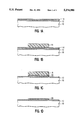
- FIGS. 1A through 1E illustrate in schematic form the steps employed in the method of manufacturing a microfuse in accord with the present invention
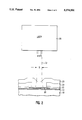
- FIG. 2 illustrates in schematic form a method of deleting a microfuse in accord with the present invention
- FIGS. 3 and 4 illustrate top schematic views of microfuse shapes and dimensions in accord with the present invention.
- FIG. 5 illustrates a top schematic view of a method of deleting a microfuse in accord with the present invention.
- the surface of a substrate 10 is cleaned, for example, in a BHF bath, and then in-situ sputter cleaned.
- a thin film 12 of a passivation layer, such as silicon dioxide, is preferably grown on the clean surface of substrate 10.
- a fusible film 14 is deposited on the passivation layer 12 by the sputter deposition, preferably, of a SiCr film to a thickness, preferably in the range of 300 angstroms to 750 angstroms from a target composed preferably of approximately 28 percent Cr and 72 percent Si.
- the film is amorphous as deposited. It transforms to a polycrystalline structure after being annealed at or above 280° C. for 30 minutes or longer.
- the polycrystalline film consists of chromium disilicide (CrSi2) supersaturated with Si soluble atoms.
- a fuse pattern in photoresist layer 16 is defined on the surface of the SiCr layer 14 using standard photolithographic techniques.
- the particular parameters used to define the features of each fuse in layer 16 are a critical feature of the present invention and will be described in more detail in connection with FIGS. 2, 3, 4, and 5.
- the exposed surface of the SiCr layer 14 is etched away, preferably using a reactive ion etching (also called plasma etching) technique in an O2/CF4 mixture to define the fuse pattern 20.
- the photoresist 16 is then removed, as shown in FIG. 1D thereby exposing the fuse pattern 20.
- the fuse pattern 20 includes a plurality of microfuses, each containing a fusible link.
- the fuse layer 20 is sputter cleaned and then a final metallization layer is deposited over the surface of the substrate 10 and the microfuse pattern 20.
- the final metallization layer is preferably a bi-layer formed by first in-situ depositing a layer 22 of tungsten to a thickness of approximately 100 nanometers, completely covering the surface.
- a final layer 24 of an aluminum alloy, for example, the Ti/AlCu/Ti/AlCu alloy called TACTAC is deposited by sputtering over the entire surface of the tungsten layer 22. Using standard photolithographic techniques, the final metal pattern is shown.
- the resulting structure is now annealed at a temperature in the range of 350° C.-450° C. for a period of 30-90 minutes. Then a final passivation layer 26 of SiO2 is deposited over the entire surface of the structure to a thickness of at least 3.0 ⁇ m.
- a laser 30 is positioned at a predetermined distance from the microfuse pattern 20 thereby establishing the accuracy at which a laser beam can be directed at a particular microfuse.
- Laser 30 is preferably a YAG infra-red laser admitting light at a wave length of 1.064 ⁇ m in a focused columnar laser beam 32 having a diameter D.
- the diameter D of beam 32 is predetermined.
- a first microfuse 40 is shown having a rectangular shape wherein the length L 1 is determined by the distance between the metallization terminals 42.
- the fuse link 40 has a width W 1 .
- a preferred embodiment of a microfuse 50 is barbell shaped and includes a fuse link portion 52 having a length L 2 determined by the distance between flared portions 54.
- the flared portions 54 are in turn connected to metallization terminals 56.
- the fuse link 52 has a width W 2 .
- the photoresist 16 defines a fuse pattern 20 wherein each fuse has a fusible link portion 40 or 52, as shown in FIGS. 3 and 4, having a length at least equal to the sum of the predetermined laser spot diameter D and the predetermined laser beam alignment accuracy.
- the width of the fusible link is defined to be no greater than half the predetermined laser spot diameter D as shown in FIG. 5.
- the passivation layer 26 has a refraction or interference effect on the beam 32, causing the spot diameter to increase at the plane of pattern 20.
- the diameter D of the laser beam 32 is preferably adjustable and the microfuse has a predetermined composition, length, and width, and is covered with a passivation layer, having a thickness of at least 3 ⁇ m as shown in FIG. 2.
- the beam 32 has an inherent accuracy with respect to the target fuse pattern 20 at a given distance between the laser 30 and the fuse pattern 20.
- the diameter of the laser beam may then be adjusted so that the minimum diameter is at least equal to W+ ⁇ P w where W equals the width of the microfuse, shown in FIG. 5, and ⁇ P w equals the accuracy of the laser beam in the direction of W.
- the maximum diameter of the beam is preferably L+ ⁇ P L where L equals the length of the microfuse shown in FIG. 5 and ⁇ P L equals the accuracy of the beam in the direction of L.
- the direction of L coincides with the axis 58 of the fuse link 52 or 40 and is perpindicular to the direction of W.
- the axis 58 bisects the width W and is parallel to the length L of the link 52 or 40.
- the adjusted laser beam is directed at the microfuse through the passivation layer 26 at a predetermined energy level to delete the microfuse.
- the predetermined energy level is preferably between 0.5 and 0.6 ⁇ J.
- such laser pulses have a duration of between 10 and 100 nanoseconds and preferably approximately 15 to 30 nanoseconds.
- the preferred method of practicing this embodiment of the invention is to direct three distinct beams at the microfuse, wherein the first beam 60 is directed at the center 62 of the microfuse.
- a second beam 64 equal in strength to the first beam 60, is then directed through the passivation layer 26 at a point 66 on the microfuse offset from the center 62 of the microfuse in the direction of W, perpindicular to the axis 58, preferably between one half the minimum beam diameter and one half the maximum beam diameter.
- a third adjusted laser beam 68 is directed at the microfuse through the passivation layer 26 at a point 70 on the microfuse offset from the center 60 by between one half the minimum beam diameter and one half the maximum beam diameter also in the direction of W but opposite to the offset of the second beam 64.
- TABLE I shows an example of the relationship between beam size and yield--i.e. the percentage of successfully deleted fuses--used in establishing the beam size parameters of the present invention.
Abstract
A method of fabricating a microfuse, deletable by laser pulses utilizes laser pulses of a predetermined spot diameter and beam alignment accuracy. A fusible link forming a portion of the microfuse is defined such that its length is at least equal to the sum of the laser spot diameter and the beam alignment accuracy and its width is no greater than half the laser spot diameter. A method of deleting the microfuse by laser pulses is provided where the microfuse has a predetermined composition, length and width having an axis bisecting the width and parallel to the length and is covered with a passivation layer at least 3 μm thick. The method includes adjusting the diameter of the beam of laser light (i) to at least a minimum diameter of W+ΔPw, where W equals the width of the microfuse fuse link and Δ Pw equals the accuracy of the beam in the direction of W and (ii) to no more than a maximum diameter of L+ΔPL, where L equals the length of the microfuse fuse link and ΔPL equals the accuracy of the beam in the direction of L.
Description
This application is related to U.S. patent application Ser. No. 07/990,679 filed Dec. 15, 1992, and entitled "Structure and Fabrication of SiCr Microfuses", assigned to the assignee of the present invention.
The present invention relates generally to the fabrication and laser deletion of microfuses and more particularly to a process for fabricating a microfuse within an integrated circuit and deleting such microfuse by one or more laser pulses.
The use of microfuses in digital integrated circuits is well known for the purpose of selectively disconnecting unwanted components from the circuit. A known technique for deleting such fuses from the circuit involves the application of a laser light beam to the microfuse fuse link having sufficient energy to melt the fuse link. Such a technique has traditionally involved reducing or removing any passivation oxide present over the fuse link structure, thereby creating a window to facilitate the deletion of the fuse. During the fuse-deletion process, a crater is typically formed exposing the remains of the disintegrated fuse to the surrounding area. This process has the potential to cause many adverse effects to the portion of the integrated circuit in proximity to the deleted fuse, such as delamination of the circuit, contamination of the circuit with deleted particles, and corrosion. In addition, it has been difficult to obtain a satisfactory yield of deleted fuses using such prior techniques.
A feature of the present invention is the provision of a process for deleting microfuses from an integrated circuit structure with a laser light source which eliminates the need for opening a window to gain access to the fuse.
Another feature of the present invention is the provision of such a method of deleting a microfuse for interconnecting the components of an integrated circuit in a desired manner which yields a high rate of deleted fuses.
A further feature of the present invention is the provision of such a method of deleting microfuses for interconnecting the components of an integrated circuit in a desired manner which eliminates adverse effects to the surrounding integrated circuit areas such as delamination, contamination, and corrosion.
Yet another feature of the present invention is a method of fabricating a microfuse which is deletable by laser pulses of a predetermined spot diameter and beam alignment accuracy to achieve the aforementioned features.
Accordingly, a method of fabricating a microfuse deletable by laser pulses of a predetermined spot diameter and beam alignment accuracy is provided for interconnecting the components of an integrated circuit in a desired manner. The method includes the steps of: (a) depositing a fusible film on a substrate to a predetermined thickness; (b) depositing a mask layer of photoresist material on the fusib le film layer to define the size of a fusible link forming a portion of the microfuse, such that the length of the fusible link is at least equal to the sum of the predetermined laser spot diameter and the predetermined beam alignment accuracy, and such that the width of the fusible link is no greater than half the predetermined laser spot diameter; and, (c) etching away a portion of the fusible film layer exposed by the photoresist mask thereby forming the microfuse including the fusible link.
Additionally, a method of deleting a microfuse for interconnecting the components of an integrated circuit in a desired manner is provided wherein the microfuse has a predetermined composition, length and width, and an axis bisecting the width and parallel to the length, and is covered by a passivation layer having a thickness of at least three micrometers. The method includes the steps of: (a) generating a beam of laser light from having an adjustable diameter and an inherent accuracy with respect to a target at a given distance; (b) positioning the laser source at a predetermined distance from the microfuse thereby establishing the accuracy at which the beam can be directed at the microfuse; (c) adjusting the diameter of the beam (i) to at least a minimum diameter of W+ΔPL, where W equals the width of the microfuse fuse link and ΔP equals the accuracy of the beam in a direction perpendicular to the link axis and (ii) to no more than a maximum diameter of L+ΔPL, where L equals the length of the microfuse fuse link and Δ PL equals the accuracy of the beam in a direction parallel to the link axis; and (d) directing the adjusted laser beam at the microfuse fuse link through the passivation layer at a predetermined energy level to thereby delete the microfuse.
Other advantages and novel features of the present invention will become apparent from the following detailed description of the invention when considered in conjunction with the accompanying drawings.
FIGS. 1A through 1E illustrate in schematic form the steps employed in the method of manufacturing a microfuse in accord with the present invention;
FIG. 2 illustrates in schematic form a method of deleting a microfuse in accord with the present invention;
FIGS. 3 and 4 illustrate top schematic views of microfuse shapes and dimensions in accord with the present invention; and
FIG. 5 illustrates a top schematic view of a method of deleting a microfuse in accord with the present invention.
Referring now to the drawings, the invention will first be described in connection with fabricating a microfuse which is deletable by laser pulses of a predetermined spot diameter and beam accuracy. The basic fabrication steps are the same as those described and claimed in U.S. application Ser. No. 07/990,679 to Carruthers, et al, filed Dec. 15, 1992, and assigned to the assignee of the present invention.
Referring to FIG. 1A, the surface of a substrate 10 is cleaned, for example, in a BHF bath, and then in-situ sputter cleaned. A thin film 12 of a passivation layer, such as silicon dioxide, is preferably grown on the clean surface of substrate 10. A fusible film 14 is deposited on the passivation layer 12 by the sputter deposition, preferably, of a SiCr film to a thickness, preferably in the range of 300 angstroms to 750 angstroms from a target composed preferably of approximately 28 percent Cr and 72 percent Si. The film is amorphous as deposited. It transforms to a polycrystalline structure after being annealed at or above 280° C. for 30 minutes or longer. The polycrystalline film consists of chromium disilicide (CrSi2) supersaturated with Si soluble atoms.
As shown in FIG. 1B, a fuse pattern in photoresist layer 16 is defined on the surface of the SiCr layer 14 using standard photolithographic techniques. The particular parameters used to define the features of each fuse in layer 16 are a critical feature of the present invention and will be described in more detail in connection with FIGS. 2, 3, 4, and 5.
As shown in FIG. 1C, the exposed surface of the SiCr layer 14 is etched away, preferably using a reactive ion etching (also called plasma etching) technique in an O2/CF4 mixture to define the fuse pattern 20. The photoresist 16 is then removed, as shown in FIG. 1D thereby exposing the fuse pattern 20. The fuse pattern 20 includes a plurality of microfuses, each containing a fusible link.
As shown in FIG. 1E, the remaining steps of the microfuse fabrication process of the present invention will be described. The fuse layer 20 is sputter cleaned and then a final metallization layer is deposited over the surface of the substrate 10 and the microfuse pattern 20. The final metallization layer is preferably a bi-layer formed by first in-situ depositing a layer 22 of tungsten to a thickness of approximately 100 nanometers, completely covering the surface. A final layer 24 of an aluminum alloy, for example, the Ti/AlCu/Ti/AlCu alloy called TACTAC is deposited by sputtering over the entire surface of the tungsten layer 22. Using standard photolithographic techniques, the final metal pattern is shown.
The resulting structure is now annealed at a temperature in the range of 350° C.-450° C. for a period of 30-90 minutes. Then a final passivation layer 26 of SiO2 is deposited over the entire surface of the structure to a thickness of at least 3.0 μm.
Referring to FIG. 2 to further understand the method heretofore described, a laser 30 is positioned at a predetermined distance from the microfuse pattern 20 thereby establishing the accuracy at which a laser beam can be directed at a particular microfuse. Laser 30 is preferably a YAG infra-red laser admitting light at a wave length of 1.064 μm in a focused columnar laser beam 32 having a diameter D. In the method described in connection with FIGS. 1A-E, the diameter D of beam 32 is predetermined.
Referring to FIG. 3, a first microfuse 40 is shown having a rectangular shape wherein the length L1 is determined by the distance between the metallization terminals 42. The fuse link 40 has a width W1. In FIG. 4 a preferred embodiment of a microfuse 50 is barbell shaped and includes a fuse link portion 52 having a length L2 determined by the distance between flared portions 54. The flared portions 54 are in turn connected to metallization terminals 56. The fuse link 52 has a width W2.
Referring to FIGS. 1B and 1C, the photoresist 16 defines a fuse pattern 20 wherein each fuse has a fusible link portion 40 or 52, as shown in FIGS. 3 and 4, having a length at least equal to the sum of the predetermined laser spot diameter D and the predetermined laser beam alignment accuracy. The width of the fusible link is defined to be no greater than half the predetermined laser spot diameter D as shown in FIG. 5. As is shown in FIG. 2, the passivation layer 26 has a refraction or interference effect on the beam 32, causing the spot diameter to increase at the plane of pattern 20.
In a second embodiment of the present invention, a method is provided for deleting a microfuse interconnecting the components of an integrated circuit in a desired manner. In this embodiment, the diameter D of the laser beam 32 is preferably adjustable and the microfuse has a predetermined composition, length, and width, and is covered with a passivation layer, having a thickness of at least 3 μm as shown in FIG. 2. The beam 32 has an inherent accuracy with respect to the target fuse pattern 20 at a given distance between the laser 30 and the fuse pattern 20. The diameter of the laser beam may then be adjusted so that the minimum diameter is at least equal to W+ΔPw where W equals the width of the microfuse, shown in FIG. 5, and Δ Pw equals the accuracy of the laser beam in the direction of W. The maximum diameter of the beam is preferably L+ΔPL where L equals the length of the microfuse shown in FIG. 5 and Δ PL equals the accuracy of the beam in the direction of L. The direction of L coincides with the axis 58 of the fuse link 52 or 40 and is perpindicular to the direction of W. The axis 58 bisects the width W and is parallel to the length L of the link 52 or 40. The adjusted laser beam is directed at the microfuse through the passivation layer 26 at a predetermined energy level to delete the microfuse. The predetermined energy level is preferably between 0.5 and 0.6 μJ. Preferably such laser pulses have a duration of between 10 and 100 nanoseconds and preferably approximately 15 to 30 nanoseconds. The preferred method of practicing this embodiment of the invention is to direct three distinct beams at the microfuse, wherein the first beam 60 is directed at the center 62 of the microfuse. A second beam 64, equal in strength to the first beam 60, is then directed through the passivation layer 26 at a point 66 on the microfuse offset from the center 62 of the microfuse in the direction of W, perpindicular to the axis 58, preferably between one half the minimum beam diameter and one half the maximum beam diameter. Finally, a third adjusted laser beam 68 is directed at the microfuse through the passivation layer 26 at a point 70 on the microfuse offset from the center 60 by between one half the minimum beam diameter and one half the maximum beam diameter also in the direction of W but opposite to the offset of the second beam 64.
TABLE I shows an example of the relationship between beam size and yield--i.e. the percentage of successfully deleted fuses--used in establishing the beam size parameters of the present invention.
              TABLE 1
______________________________________
YIELD (%) OF DELETED FUSES
BEAM SIZE (μM)
                3.0    5.0       6.0  9.0
______________________________________
ARRAY 1         100    84        65   79
ARRAY 2         100    *         55   66
DISCRETE        100    95        100  96
______________________________________
 Fuse Dimensions (μm): L = 3.7, W = 1.5
 ARRAY 1 = 24 Fuses/6.4 μm Pitch
 ARRAY 2 = 24 Fuses/14 μm Pitch
 *Not measured
 Δ P.sub.L = P.sub.W = 0. 5 μm
In this manner, a highly efficient process has been developed for deleting microfuses by means of a laser technique through the passivation layer of the integrated circuit containing such fuses. This process eliminates the need for opening a window in the passivation layer, yields a high rate of deleted fuses, and eliminates adverse effects to the surrounding integrated circuit areas.
While there have been described what are at present considered to be the preferred embodiments of the present invention, it will be obvious to those skilled in the art that various changes and modifictions may be made therein, without departing from the invention, and it is, therefore, aimed in the appended claims to cover all such changes and modifications as follow in the true spirit and scope of the present invention.
Claims (5)
1. A method of deleting a microfuse for interconnecting the components of an integrated circuit in a desired manner, said microfuse having a fuse link with a length and width having an axis bisecting the width and parallel to the length, and being covered by a passivation layer having a thickness of at least 3.0 μm, said method comprising the steps of:
a) generating a beam of laser light having an adjustable diameter and an inherent accuracy with respect to a target at a given distance;
b) positioning said laser source at a distance from said microfuse thereby establishing the accuracy at which said beam can be directed at said microfuse;
c) adjusting the diameter of said beam (i) to at least a minimum diameter of
W+ΔP.sub.w,
where, W equals the width of said microfuse fuse link and Δ Pw equals the accuracy of said beam in a direction perpendicular to said axis
and (ii) to no more than a maximum diameter of
L+ΔP.sub.L,
where, L equals the length of said microfuse fuse link, and
Δ PL equals the accuracy of said beam in the direction parallel to said axis, and
d) directing said adjusted laser beam at said microfuse fuse link, through said passivation layer to thereby delete said microfuse while leaving said passivation layer in place with said thickness of at least 3.0 μm.
2. The method of claim 1 wherein said adjusted laser beam energy level is between 0.5 and 0.6 μJ.
3. The method of claim 1 wherein said adjusted laser beam is directed at the center of said microfuse fuse link.
4. The method of claim 3 further including the step of:
e) directing a second said adjusted laser beam at said microfuse, through said passivation layer, wherein said second beam is directed at a point on said microfuse fuse link offset from said center by between one half said minimum beam diameter and one half said maximum beam diameter in a direction perpendicular to said axis.
5. The method of claim 4 further including the step of:
f) directing a third said adjusted laser beam at said microfuse, through said passivation layer, wherein said third beam is directed at a point on said microfuse fuse link offset from said center by between one half said minimum beam diameter and one half said maximum beam diameter, wherein said third beam is offset from said center in a direction opposite to the offset of said second beam in a direction perpendicular to said axis.
Priority Applications (3)
| Application Number | Priority Date | Filing Date | Title |
|---|---|---|---|
| US08/053,282 US5374590A (en) | 1993-04-28 | 1993-04-28 | Fabrication and laser deletion of microfuses |
| EP94480024A EP0622846A1 (en) | 1993-04-28 | 1994-03-08 | Fabrication and laser deletion of microfuses |
| JP6060973A JP2597818B2 (en) | 1993-04-28 | 1994-03-30 | How to remove microfuse |
Applications Claiming Priority (1)
| Application Number | Priority Date | Filing Date | Title |
|---|---|---|---|
| US08/053,282 US5374590A (en) | 1993-04-28 | 1993-04-28 | Fabrication and laser deletion of microfuses |
Publications (1)
| Publication Number | Publication Date |
|---|---|
| US5374590A true US5374590A (en) | 1994-12-20 |
Family
ID=21983133
Family Applications (1)
| Application Number | Title | Priority Date | Filing Date |
|---|---|---|---|
| US08/053,282 Expired - Fee Related US5374590A (en) | 1993-04-28 | 1993-04-28 | Fabrication and laser deletion of microfuses |
Country Status (3)
| Country | Link |
|---|---|
| US (1) | US5374590A (en) |
| EP (1) | EP0622846A1 (en) |
| JP (1) | JP2597818B2 (en) |
Cited By (35)
| Publication number | Priority date | Publication date | Assignee | Title |
|---|---|---|---|---|
| US5552757A (en) * | 1994-05-27 | 1996-09-03 | Littelfuse, Inc. | Surface-mounted fuse device |
| US5581225A (en) * | 1995-04-20 | 1996-12-03 | Littelfuse, Inc. | One-piece female blade fuse with housing |
| US5668521A (en) * | 1995-03-22 | 1997-09-16 | Littelfuse, Inc. | Three piece female blade fuse assembly having fuse link terminal with a clip receiving portion |
| US5675174A (en) * | 1993-01-06 | 1997-10-07 | Rohm Co., Ltd. | Method for using fuse structure in semiconductor device |
| US5699032A (en) * | 1996-06-07 | 1997-12-16 | Littelfuse, Inc. | Surface-mount fuse having a substrate with surfaces and a metal strip attached to the substrate using layer of adhesive material |
| US5790008A (en) * | 1994-05-27 | 1998-08-04 | Littlefuse, Inc. | Surface-mounted fuse device with conductive terminal pad layers and groove on side surfaces |
| WO1998044550A1 (en) * | 1997-04-03 | 1998-10-08 | Massachusetts Institute Of Technology | Laser-induced cutting of metal interconnect |
| US5886612A (en) * | 1997-10-20 | 1999-03-23 | Littelfuse, Inc. | Female fuse housing |
| US5929740A (en) * | 1997-10-20 | 1999-07-27 | Littelfuse, Inc. | One-piece female blade fuse with housing and improvements thereof |
| US5936296A (en) * | 1997-06-23 | 1999-08-10 | Samsung Electronics Co., Ltd. | Integrated circuits having metallic fuse links |
| US5974661A (en) * | 1994-05-27 | 1999-11-02 | Littelfuse, Inc. | Method of manufacturing a surface-mountable device for protection against electrostatic damage to electronic components |
| US5977860A (en) * | 1996-06-07 | 1999-11-02 | Littelfuse, Inc. | Surface-mount fuse and the manufacture thereof |
| US6063651A (en) * | 1998-02-03 | 2000-05-16 | International Business Machines Corporation | Method for activating fusible links on a circuit substrate |
| US6163062A (en) * | 1997-10-27 | 2000-12-19 | Mitsubishi Denki Kabushiki Kaisha | Semiconductor device having a metallic fuse member and cutting method thereof with laser light |
| US6191928B1 (en) | 1994-05-27 | 2001-02-20 | Littelfuse, Inc. | Surface-mountable device for protection against electrostatic damage to electronic components |
| US6217151B1 (en) | 1998-06-18 | 2001-04-17 | Xerox Corporation | Controlling AIP print uniformity by adjusting row electrode area and shape |
| US20030011026A1 (en) * | 2001-07-10 | 2003-01-16 | Colby James A. | Electrostatic discharge apparatus for network devices |
| US20030025587A1 (en) * | 2001-07-10 | 2003-02-06 | Whitney Stephen J. | Electrostatic discharge multifunction resistor |
| US20030166352A1 (en) * | 2002-03-04 | 2003-09-04 | Seibang Oh | Multi-element fuse array |
| US20050190519A1 (en) * | 2003-11-26 | 2005-09-01 | Brown William P. | Vehicle electrical protection device and system employing same |
| US20060028655A1 (en) * | 2001-03-29 | 2006-02-09 | Gsil Lumonics Corporation | Methods and systems for precisely relatively positioning a waist of a pulsed laser beam and method and system for controlling energy delivered to a target structure |
| US20060205121A1 (en) * | 2002-03-27 | 2006-09-14 | Gsi Lumonics Corporation | Method and system for high-speed, precise micromachining an array of devices |
| US20070178714A1 (en) * | 2002-03-27 | 2007-08-02 | Bo Gu | Method and system for high-speed precise laser trimming and scan lens for use therein |
| US20070215575A1 (en) * | 2006-03-15 | 2007-09-20 | Bo Gu | Method and system for high-speed, precise, laser-based modification of one or more electrical elements |
| CN100361300C (en) * | 2003-06-24 | 2008-01-09 | 三星电子株式会社 | Integrated circuit devices having corrosion resistant fuse regions and methods of fabricating the same |
| US20080029491A1 (en) * | 2006-07-20 | 2008-02-07 | Gsi Group Corporation | System and method for laser processing at non-constant velocities |
| US7482551B2 (en) | 2000-01-10 | 2009-01-27 | Electro Scientific Industries, Inc. | Processing a memory link with a set of at least two laser pulses |
| US7582848B2 (en) | 1999-12-28 | 2009-09-01 | Gsi Group Corp | Energy-efficient, laser-based method and system for processing target material |
| US7723642B2 (en) | 1999-12-28 | 2010-05-25 | Gsi Group Corporation | Laser-based system for memory link processing with picosecond lasers |
| US7838794B2 (en) | 1999-12-28 | 2010-11-23 | Gsi Group Corporation | Laser-based method and system for removing one or more target link structures |
| US7843308B2 (en) | 2002-04-08 | 2010-11-30 | Littlefuse, Inc. | Direct application voltage variable material |
| US7983024B2 (en) | 2007-04-24 | 2011-07-19 | Littelfuse, Inc. | Fuse card system for automotive circuit protection |
| US20110210105A1 (en) * | 2009-12-30 | 2011-09-01 | Gsi Group Corporation | Link processing with high speed beam deflection |
| US8339235B2 (en) | 2008-08-06 | 2012-12-25 | Beckert James J | Housing securing apparatus for electrical components, especially fuses |
| CN106384699A (en) * | 2016-11-24 | 2017-02-08 | 深圳路科技有限公司 | Method for manufacturing fuses by using LDS technology |
Citations (11)
| Publication number | Priority date | Publication date | Assignee | Title |
|---|---|---|---|---|
| US4240094A (en) * | 1978-03-20 | 1980-12-16 | Harris Corporation | Laser-configured logic array |
| US4338590A (en) * | 1980-01-07 | 1982-07-06 | National Semiconductor Corporation | Multi stage resistive ladder network having extra stages for trimming |
| US4387503A (en) * | 1981-08-13 | 1983-06-14 | Mostek Corporation | Method for programming circuit elements in integrated circuits |
| EP0090565A2 (en) * | 1982-03-30 | 1983-10-05 | Fujitsu Limited | Process for selectively cutting an electrical conductive layer by irradiation with an energy beam |
| JPS61194740A (en) * | 1985-02-25 | 1986-08-29 | Hitachi Ltd | Semiconductor device |
| JPS6216544A (en) * | 1985-07-15 | 1987-01-24 | Mitsubishi Electric Corp | Fuse for redundancy circuit |
| US4745258A (en) * | 1985-08-27 | 1988-05-17 | Mitsubishi Denki Kabushiki Kaisha | Apparatus for laser-cutting metal interconnections in a semiconductor device |
| EP0272799A1 (en) * | 1986-11-26 | 1988-06-29 | Quick Technologies Ltd. | Ablative etch resistant coating for laser personalization of integrated circuits |
| US4862243A (en) * | 1987-06-01 | 1989-08-29 | Texas Instruments Incorporated | Scalable fuse link element |
| US4882293A (en) * | 1987-09-19 | 1989-11-21 | Texas Instruments Deutschland Gmbh | Method of making an electrically programmable integrated circuit containing meltable contact bridges |
| US5096850A (en) * | 1991-04-23 | 1992-03-17 | Harris Corporation | Method of laser trimming |
Family Cites Families (3)
| Publication number | Priority date | Publication date | Assignee | Title |
|---|---|---|---|---|
| US4238839A (en) * | 1979-04-19 | 1980-12-09 | National Semiconductor Corporation | Laser programmable read only memory |
| JPS5775442A (en) * | 1980-10-29 | 1982-05-12 | Toshiba Corp | Semiconductor device |
| JP2728412B2 (en) * | 1987-12-25 | 1998-03-18 | 株式会社日立製作所 | Semiconductor device |
-
1993
- 1993-04-28 US US08/053,282 patent/US5374590A/en not_active Expired - Fee Related
-
1994
- 1994-03-08 EP EP94480024A patent/EP0622846A1/en not_active Withdrawn
- 1994-03-30 JP JP6060973A patent/JP2597818B2/en not_active Expired - Lifetime
Patent Citations (12)
| Publication number | Priority date | Publication date | Assignee | Title |
|---|---|---|---|---|
| US4240094A (en) * | 1978-03-20 | 1980-12-16 | Harris Corporation | Laser-configured logic array |
| US4338590A (en) * | 1980-01-07 | 1982-07-06 | National Semiconductor Corporation | Multi stage resistive ladder network having extra stages for trimming |
| US4387503A (en) * | 1981-08-13 | 1983-06-14 | Mostek Corporation | Method for programming circuit elements in integrated circuits |
| EP0090565A2 (en) * | 1982-03-30 | 1983-10-05 | Fujitsu Limited | Process for selectively cutting an electrical conductive layer by irradiation with an energy beam |
| US4476375A (en) * | 1982-03-30 | 1984-10-09 | Fujitsu Limited | Process for selective cutting of electrical conductive layer by irradiation of energy beam |
| JPS61194740A (en) * | 1985-02-25 | 1986-08-29 | Hitachi Ltd | Semiconductor device |
| JPS6216544A (en) * | 1985-07-15 | 1987-01-24 | Mitsubishi Electric Corp | Fuse for redundancy circuit |
| US4745258A (en) * | 1985-08-27 | 1988-05-17 | Mitsubishi Denki Kabushiki Kaisha | Apparatus for laser-cutting metal interconnections in a semiconductor device |
| EP0272799A1 (en) * | 1986-11-26 | 1988-06-29 | Quick Technologies Ltd. | Ablative etch resistant coating for laser personalization of integrated circuits |
| US4862243A (en) * | 1987-06-01 | 1989-08-29 | Texas Instruments Incorporated | Scalable fuse link element |
| US4882293A (en) * | 1987-09-19 | 1989-11-21 | Texas Instruments Deutschland Gmbh | Method of making an electrically programmable integrated circuit containing meltable contact bridges |
| US5096850A (en) * | 1991-04-23 | 1992-03-17 | Harris Corporation | Method of laser trimming |
Non-Patent Citations (4)
| Title |
|---|
| Related U.S. patent application Ser. No. 07/990,679 filed Dec. 15, 1992 entitled "Structure and Fabrication of SiCr Microfuses" IBM Docket No. FI9-90-054. |
| Related U.S. patent application Ser. No. 07/990,679 filed Dec. 15, 1992 entitled Structure and Fabrication of SiCr Microfuses IBM Docket No. FI9 90 054. * |
| S. Wolf et al. Silicon Processing for the VLSI ERA vol. I: Process Technology Lattice Press, Sunset Beach, Calif. 1986 pp. 407 409. * |
| S. Wolf et al. Silicon Processing for the VLSI ERA vol. I: Process Technology Lattice Press, Sunset Beach, Calif. 1986 pp. 407-409. |
Cited By (61)
| Publication number | Priority date | Publication date | Assignee | Title |
|---|---|---|---|---|
| US5675174A (en) * | 1993-01-06 | 1997-10-07 | Rohm Co., Ltd. | Method for using fuse structure in semiconductor device |
| US5974661A (en) * | 1994-05-27 | 1999-11-02 | Littelfuse, Inc. | Method of manufacturing a surface-mountable device for protection against electrostatic damage to electronic components |
| US5790008A (en) * | 1994-05-27 | 1998-08-04 | Littlefuse, Inc. | Surface-mounted fuse device with conductive terminal pad layers and groove on side surfaces |
| US6191928B1 (en) | 1994-05-27 | 2001-02-20 | Littelfuse, Inc. | Surface-mountable device for protection against electrostatic damage to electronic components |
| US5844477A (en) * | 1994-05-27 | 1998-12-01 | Littelfuse, Inc. | Method of protecting a surface-mount fuse device |
| US5552757A (en) * | 1994-05-27 | 1996-09-03 | Littelfuse, Inc. | Surface-mounted fuse device |
| US6023028A (en) * | 1994-05-27 | 2000-02-08 | Littelfuse, Inc. | Surface-mountable device having a voltage variable polgmeric material for protection against electrostatic damage to electronic components |
| US5943764A (en) * | 1994-05-27 | 1999-08-31 | Littelfuse, Inc. | Method of manufacturing a surface-mounted fuse device |
| US5668521A (en) * | 1995-03-22 | 1997-09-16 | Littelfuse, Inc. | Three piece female blade fuse assembly having fuse link terminal with a clip receiving portion |
| US5581225A (en) * | 1995-04-20 | 1996-12-03 | Littelfuse, Inc. | One-piece female blade fuse with housing |
| US5699032A (en) * | 1996-06-07 | 1997-12-16 | Littelfuse, Inc. | Surface-mount fuse having a substrate with surfaces and a metal strip attached to the substrate using layer of adhesive material |
| US5977860A (en) * | 1996-06-07 | 1999-11-02 | Littelfuse, Inc. | Surface-mount fuse and the manufacture thereof |
| US6057221A (en) * | 1997-04-03 | 2000-05-02 | Massachusetts Institute Of Technology | Laser-induced cutting of metal interconnect |
| WO1998044550A1 (en) * | 1997-04-03 | 1998-10-08 | Massachusetts Institute Of Technology | Laser-induced cutting of metal interconnect |
| US5936296A (en) * | 1997-06-23 | 1999-08-10 | Samsung Electronics Co., Ltd. | Integrated circuits having metallic fuse links |
| US5929740A (en) * | 1997-10-20 | 1999-07-27 | Littelfuse, Inc. | One-piece female blade fuse with housing and improvements thereof |
| US5886612A (en) * | 1997-10-20 | 1999-03-23 | Littelfuse, Inc. | Female fuse housing |
| US6163062A (en) * | 1997-10-27 | 2000-12-19 | Mitsubishi Denki Kabushiki Kaisha | Semiconductor device having a metallic fuse member and cutting method thereof with laser light |
| US6063651A (en) * | 1998-02-03 | 2000-05-16 | International Business Machines Corporation | Method for activating fusible links on a circuit substrate |
| US6301903B1 (en) | 1998-02-03 | 2001-10-16 | International Business Machines Corporation | Apparatus for activating fusible links on a circuit substrate |
| US6217151B1 (en) | 1998-06-18 | 2001-04-17 | Xerox Corporation | Controlling AIP print uniformity by adjusting row electrode area and shape |
| US7750268B2 (en) | 1999-12-28 | 2010-07-06 | Gsi Group Corporation | Energy efficient, laser-based method and system for processing target material |
| US8253066B2 (en) | 1999-12-28 | 2012-08-28 | Gsi Group Corporation | Laser-based method and system for removing one or more target link structures |
| US7838794B2 (en) | 1999-12-28 | 2010-11-23 | Gsi Group Corporation | Laser-based method and system for removing one or more target link structures |
| US7723642B2 (en) | 1999-12-28 | 2010-05-25 | Gsi Group Corporation | Laser-based system for memory link processing with picosecond lasers |
| US7679030B2 (en) | 1999-12-28 | 2010-03-16 | Gsi Group Corporation | Energy-efficient, laser-based method and system for processing target material |
| US7582848B2 (en) | 1999-12-28 | 2009-09-01 | Gsi Group Corp | Energy-efficient, laser-based method and system for processing target material |
| US7482551B2 (en) | 2000-01-10 | 2009-01-27 | Electro Scientific Industries, Inc. | Processing a memory link with a set of at least two laser pulses |
| US8338746B2 (en) | 2000-01-10 | 2012-12-25 | Electro Scientific Industries, Inc. | Method for processing a memory link with a set of at least two laser pulses |
| US7671295B2 (en) | 2000-01-10 | 2010-03-02 | Electro Scientific Industries, Inc. | Processing a memory link with a set of at least two laser pulses |
| US7955906B2 (en) * | 2001-03-29 | 2011-06-07 | Gsi Group Corporation | Methods and systems for thermal-based laser processing a multi-material device |
| US20060028655A1 (en) * | 2001-03-29 | 2006-02-09 | Gsil Lumonics Corporation | Methods and systems for precisely relatively positioning a waist of a pulsed laser beam and method and system for controlling energy delivered to a target structure |
| US8809734B2 (en) | 2001-03-29 | 2014-08-19 | Electron Scientific Industries, Inc. | Methods and systems for thermal-based laser processing a multi-material device |
| US8217304B2 (en) | 2001-03-29 | 2012-07-10 | Gsi Group Corporation | Methods and systems for thermal-based laser processing a multi-material device |
| US20070215820A1 (en) * | 2001-03-29 | 2007-09-20 | Cordingley James J | Methods and systems for thermal-based laser processing a multi-material device |
| US8193468B2 (en) | 2001-03-29 | 2012-06-05 | Gsi Group Corporation | Methods and systems for precisely relatively positioning a waist of a pulsed laser beam and method and system for controlling energy delivered to a target structure |
| US7955905B2 (en) | 2001-03-29 | 2011-06-07 | Gsi Group Corporation | Methods and systems for thermal-based laser processing a multi-material device |
| US20080094640A1 (en) * | 2001-03-29 | 2008-04-24 | Cordingley James J | Methods and systems for precisely relatively positioning a waist of a pulsed laser beam and method for controlling energy delivered to a target structure |
| US20060207975A1 (en) * | 2001-03-29 | 2006-09-21 | Gsi Lumonics Corporation | High-speed, precision, laser-based method and system for processing material of one or more targets within a field |
| US20030011026A1 (en) * | 2001-07-10 | 2003-01-16 | Colby James A. | Electrostatic discharge apparatus for network devices |
| US20030025587A1 (en) * | 2001-07-10 | 2003-02-06 | Whitney Stephen J. | Electrostatic discharge multifunction resistor |
| US7034652B2 (en) | 2001-07-10 | 2006-04-25 | Littlefuse, Inc. | Electrostatic discharge multifunction resistor |
| US7035072B2 (en) | 2001-07-10 | 2006-04-25 | Littlefuse, Inc. | Electrostatic discharge apparatus for network devices |
| US20030166352A1 (en) * | 2002-03-04 | 2003-09-04 | Seibang Oh | Multi-element fuse array |
| US6878004B2 (en) | 2002-03-04 | 2005-04-12 | Littelfuse, Inc. | Multi-element fuse array |
| US7666759B2 (en) | 2002-03-27 | 2010-02-23 | Gsi Lumonics Corporation | Method and system for high-speed, precise micromachining an array of devices |
| US7563695B2 (en) | 2002-03-27 | 2009-07-21 | Gsi Group Corporation | Method and system for high-speed precise laser trimming and scan lens for use therein |
| US7871903B2 (en) | 2002-03-27 | 2011-01-18 | Gsi Group Corporation | Method and system for high-speed, precise micromachining an array of devices |
| US20070178714A1 (en) * | 2002-03-27 | 2007-08-02 | Bo Gu | Method and system for high-speed precise laser trimming and scan lens for use therein |
| US20060205121A1 (en) * | 2002-03-27 | 2006-09-14 | Gsi Lumonics Corporation | Method and system for high-speed, precise micromachining an array of devices |
| US7843308B2 (en) | 2002-04-08 | 2010-11-30 | Littlefuse, Inc. | Direct application voltage variable material |
| CN100361300C (en) * | 2003-06-24 | 2008-01-09 | 三星电子株式会社 | Integrated circuit devices having corrosion resistant fuse regions and methods of fabricating the same |
| US7233474B2 (en) | 2003-11-26 | 2007-06-19 | Littelfuse, Inc. | Vehicle electrical protection device and system employing same |
| US20050190519A1 (en) * | 2003-11-26 | 2005-09-01 | Brown William P. | Vehicle electrical protection device and system employing same |
| US20070215575A1 (en) * | 2006-03-15 | 2007-09-20 | Bo Gu | Method and system for high-speed, precise, laser-based modification of one or more electrical elements |
| US8084706B2 (en) | 2006-07-20 | 2011-12-27 | Gsi Group Corporation | System and method for laser processing at non-constant velocities |
| US20080029491A1 (en) * | 2006-07-20 | 2008-02-07 | Gsi Group Corporation | System and method for laser processing at non-constant velocities |
| US7983024B2 (en) | 2007-04-24 | 2011-07-19 | Littelfuse, Inc. | Fuse card system for automotive circuit protection |
| US8339235B2 (en) | 2008-08-06 | 2012-12-25 | Beckert James J | Housing securing apparatus for electrical components, especially fuses |
| US20110210105A1 (en) * | 2009-12-30 | 2011-09-01 | Gsi Group Corporation | Link processing with high speed beam deflection |
| CN106384699A (en) * | 2016-11-24 | 2017-02-08 | 深圳路科技有限公司 | Method for manufacturing fuses by using LDS technology |
Also Published As
| Publication number | Publication date |
|---|---|
| JP2597818B2 (en) | 1997-04-09 |
| EP0622846A1 (en) | 1994-11-02 |
| JPH06314535A (en) | 1994-11-08 |
Similar Documents
| Publication | Publication Date | Title |
|---|---|---|
| US5374590A (en) | Fabrication and laser deletion of microfuses | |
| US5329152A (en) | Ablative etch resistant coating for laser personalization of integrated circuits | |
| DE19782235B4 (en) | Laser-based method and system for repair or reconfiguration of an integrated circuit | |
| US5369053A (en) | Method for patterning aluminum metallizations | |
| WO2006032335A1 (en) | Saw-component having a reduced temperature path and method for the production thereof | |
| JPS58169940A (en) | Manufacture of semiconductor device | |
| JP2769332B2 (en) | Manufacturing electrically programmable integrated circuits. | |
| US5899728A (en) | Method of forming a lithographic mask | |
| US4549064A (en) | Laser treatment of silicon nitride | |
| US5288664A (en) | Method of forming wiring of semiconductor device | |
| EP0113522A2 (en) | The manufacture of semiconductor devices | |
| EP0272799A1 (en) | Ablative etch resistant coating for laser personalization of integrated circuits | |
| JPS63222445A (en) | Bump-electrode forming method | |
| JPS59126634A (en) | Formation of pattern | |
| JPH05114558A (en) | Manufacture of semiconductor device | |
| CN116676571B (en) | Electrode manufacturing method, electrode and semiconductor device | |
| JP3259730B2 (en) | X-ray mask | |
| JPH0513442A (en) | Semiconductor substrate | |
| JP2858757B2 (en) | Wiring formation method | |
| DE10316925B4 (en) | Acoustic surface wave component | |
| JPS58115835A (en) | Formation of buried wirings of semiconductor device | |
| JPH1097055A (en) | Mask for electron beam exposure and its production | |
| JPH02271631A (en) | Manufacture of semiconductor device | |
| JPS6029921B2 (en) | Diffraction grating manufacturing method | |
| JPS6017911A (en) | Manufacture of semiconductor device |
Legal Events
| Date | Code | Title | Description |
|---|---|---|---|
| AS | Assignment |
Owner name: INTERNATIONAL BUSINESS MACHINES CORPORATION, NEW Y Free format text: ASSIGNMENT OF ASSIGNORS INTEREST;ASSIGNORS:BATDORF, KERRY L.;GILMOUR, RICHARD A.;TSANG, PAUL;REEL/FRAME:006534/0979;SIGNING DATES FROM 19930421 TO 19930422 |
|
| FPAY | Fee payment |
Year of fee payment: 4 |
|
| FPAY | Fee payment |
Year of fee payment: 8 |
|
| REMI | Maintenance fee reminder mailed | ||
| LAPS | Lapse for failure to pay maintenance fees | ||
| STCH | Information on status: patent discontinuation |
Free format text: PATENT EXPIRED DUE TO NONPAYMENT OF MAINTENANCE FEES UNDER 37 CFR 1.362 |
|
| FP | Lapsed due to failure to pay maintenance fee |
Effective date: 20061220 |