US5408130A - Interconnection structure for conductive layers - Google Patents
Interconnection structure for conductive layers Download PDFInfo
- Publication number
- US5408130A US5408130A US08/286,592 US28659294A US5408130A US 5408130 A US5408130 A US 5408130A US 28659294 A US28659294 A US 28659294A US 5408130 A US5408130 A US 5408130A
- Authority
- US
- United States
- Prior art keywords
- layer
- conductive layer
- conductive
- opening
- sidewall
- Prior art date
- Legal status (The legal status is an assumption and is not a legal conclusion. Google has not performed a legal analysis and makes no representation as to the accuracy of the status listed.)
- Expired - Lifetime
Links
Images


Classifications
-
- H—ELECTRICITY
- H01—ELECTRIC ELEMENTS
- H01L—SEMICONDUCTOR DEVICES NOT COVERED BY CLASS H10
- H01L21/00—Processes or apparatus adapted for the manufacture or treatment of semiconductor or solid state devices or of parts thereof
- H01L21/70—Manufacture or treatment of devices consisting of a plurality of solid state components formed in or on a common substrate or of parts thereof; Manufacture of integrated circuit devices or of parts thereof
- H01L21/71—Manufacture of specific parts of devices defined in group H01L21/70
- H01L21/768—Applying interconnections to be used for carrying current between separate components within a device comprising conductors and dielectrics
- H01L21/76801—Applying interconnections to be used for carrying current between separate components within a device comprising conductors and dielectrics characterised by the formation and the after-treatment of the dielectrics, e.g. smoothing
- H01L21/76829—Applying interconnections to be used for carrying current between separate components within a device comprising conductors and dielectrics characterised by the formation and the after-treatment of the dielectrics, e.g. smoothing characterised by the formation of thin functional dielectric layers, e.g. dielectric etch-stop, barrier, capping or liner layers
- H01L21/76831—Applying interconnections to be used for carrying current between separate components within a device comprising conductors and dielectrics characterised by the formation and the after-treatment of the dielectrics, e.g. smoothing characterised by the formation of thin functional dielectric layers, e.g. dielectric etch-stop, barrier, capping or liner layers in via holes or trenches, e.g. non-conductive sidewall liners
-
- H—ELECTRICITY
- H01—ELECTRIC ELEMENTS
- H01L—SEMICONDUCTOR DEVICES NOT COVERED BY CLASS H10
- H01L21/00—Processes or apparatus adapted for the manufacture or treatment of semiconductor or solid state devices or of parts thereof
- H01L21/70—Manufacture or treatment of devices consisting of a plurality of solid state components formed in or on a common substrate or of parts thereof; Manufacture of integrated circuit devices or of parts thereof
- H01L21/71—Manufacture of specific parts of devices defined in group H01L21/70
- H01L21/768—Applying interconnections to be used for carrying current between separate components within a device comprising conductors and dielectrics
- H01L21/76801—Applying interconnections to be used for carrying current between separate components within a device comprising conductors and dielectrics characterised by the formation and the after-treatment of the dielectrics, e.g. smoothing
- H01L21/76802—Applying interconnections to be used for carrying current between separate components within a device comprising conductors and dielectrics characterised by the formation and the after-treatment of the dielectrics, e.g. smoothing by forming openings in dielectrics
- H01L21/76805—Applying interconnections to be used for carrying current between separate components within a device comprising conductors and dielectrics characterised by the formation and the after-treatment of the dielectrics, e.g. smoothing by forming openings in dielectrics the opening being a via or contact hole penetrating the underlying conductor
-
- H—ELECTRICITY
- H01—ELECTRIC ELEMENTS
- H01L—SEMICONDUCTOR DEVICES NOT COVERED BY CLASS H10
- H01L21/00—Processes or apparatus adapted for the manufacture or treatment of semiconductor or solid state devices or of parts thereof
- H01L21/70—Manufacture or treatment of devices consisting of a plurality of solid state components formed in or on a common substrate or of parts thereof; Manufacture of integrated circuit devices or of parts thereof
- H01L21/71—Manufacture of specific parts of devices defined in group H01L21/70
- H01L21/768—Applying interconnections to be used for carrying current between separate components within a device comprising conductors and dielectrics
- H01L21/76801—Applying interconnections to be used for carrying current between separate components within a device comprising conductors and dielectrics characterised by the formation and the after-treatment of the dielectrics, e.g. smoothing
- H01L21/76829—Applying interconnections to be used for carrying current between separate components within a device comprising conductors and dielectrics characterised by the formation and the after-treatment of the dielectrics, e.g. smoothing characterised by the formation of thin functional dielectric layers, e.g. dielectric etch-stop, barrier, capping or liner layers
- H01L21/76834—Applying interconnections to be used for carrying current between separate components within a device comprising conductors and dielectrics characterised by the formation and the after-treatment of the dielectrics, e.g. smoothing characterised by the formation of thin functional dielectric layers, e.g. dielectric etch-stop, barrier, capping or liner layers formation of thin insulating films on the sidewalls or on top of conductors
-
- H—ELECTRICITY
- H01—ELECTRIC ELEMENTS
- H01L—SEMICONDUCTOR DEVICES NOT COVERED BY CLASS H10
- H01L21/00—Processes or apparatus adapted for the manufacture or treatment of semiconductor or solid state devices or of parts thereof
- H01L21/70—Manufacture or treatment of devices consisting of a plurality of solid state components formed in or on a common substrate or of parts thereof; Manufacture of integrated circuit devices or of parts thereof
- H01L21/71—Manufacture of specific parts of devices defined in group H01L21/70
- H01L21/768—Applying interconnections to be used for carrying current between separate components within a device comprising conductors and dielectrics
- H01L21/76897—Formation of self-aligned vias or contact plugs, i.e. involving a lithographically uncritical step
-
- H—ELECTRICITY
- H01—ELECTRIC ELEMENTS
- H01L—SEMICONDUCTOR DEVICES NOT COVERED BY CLASS H10
- H01L23/00—Details of semiconductor or other solid state devices
- H01L23/48—Arrangements for conducting electric current to or from the solid state body in operation, e.g. leads, terminal arrangements ; Selection of materials therefor
- H01L23/482—Arrangements for conducting electric current to or from the solid state body in operation, e.g. leads, terminal arrangements ; Selection of materials therefor consisting of lead-in layers inseparably applied to the semiconductor body
- H01L23/485—Arrangements for conducting electric current to or from the solid state body in operation, e.g. leads, terminal arrangements ; Selection of materials therefor consisting of lead-in layers inseparably applied to the semiconductor body consisting of layered constructions comprising conductive layers and insulating layers, e.g. planar contacts
-
- H—ELECTRICITY
- H01—ELECTRIC ELEMENTS
- H01L—SEMICONDUCTOR DEVICES NOT COVERED BY CLASS H10
- H01L23/00—Details of semiconductor or other solid state devices
- H01L23/52—Arrangements for conducting electric current within the device in operation from one component to another, i.e. interconnections, e.g. wires, lead frames
- H01L23/522—Arrangements for conducting electric current within the device in operation from one component to another, i.e. interconnections, e.g. wires, lead frames including external interconnections consisting of a multilayer structure of conductive and insulating layers inseparably formed on the semiconductor body
- H01L23/5226—Via connections in a multilevel interconnection structure
-
- H—ELECTRICITY
- H01—ELECTRIC ELEMENTS
- H01L—SEMICONDUCTOR DEVICES NOT COVERED BY CLASS H10
- H01L2224/00—Indexing scheme for arrangements for connecting or disconnecting semiconductor or solid-state bodies and methods related thereto as covered by H01L24/00
- H01L2224/01—Means for bonding being attached to, or being formed on, the surface to be connected, e.g. chip-to-package, die-attach, "first-level" interconnects; Manufacturing methods related thereto
- H01L2224/02—Bonding areas; Manufacturing methods related thereto
- H01L2224/0212—Auxiliary members for bonding areas, e.g. spacers
- H01L2224/02122—Auxiliary members for bonding areas, e.g. spacers being formed on the semiconductor or solid-state body
- H01L2224/02123—Auxiliary members for bonding areas, e.g. spacers being formed on the semiconductor or solid-state body inside the bonding area
- H01L2224/02125—Reinforcing structures
- H01L2224/02126—Collar structures
-
- H—ELECTRICITY
- H01—ELECTRIC ELEMENTS
- H01L—SEMICONDUCTOR DEVICES NOT COVERED BY CLASS H10
- H01L2924/00—Indexing scheme for arrangements or methods for connecting or disconnecting semiconductor or solid-state bodies as covered by H01L24/00
- H01L2924/0001—Technical content checked by a classifier
- H01L2924/0002—Not covered by any one of groups H01L24/00, H01L24/00 and H01L2224/00
Definitions
- the present invention relates generally to semiconductor technology, and more particularly, to conductive layer interconnects.
- integrated circuits contain four or more conductive layers which overlie the substrate.
- the conductive layers are used for electrical routing of integrated circuit devices and device formation.
- a top conductive layer i.e. a fourth or a fifth conductive layer
- a lower conductive layer i.e. a first, a second conductive layer, or a diffusion.
- These contacts or interconnects are difficult to form if the intermediate layers (i.e. a third conductive layer) are positioned in close proximity to where the contact or interconnect is to be formed.
- the fourth conductive layer is electrically connected to the third conductive layer
- the third layer is electrically connected to the second layer
- the second conductive layer is electrically connected to the first conductive layer to complete the electrical contact.
- conductive layer two may be laid out within certain predetermined distances or separations from the contact region. Therefore, conductive layer three connects directly to conductive layer one without the use of conductive layer two. Disadvantages to this approach include the fact that the above-mentioned predetermined distances are lithographic tolerance defined and therefore relatively large, the contact is not self aligned, a total surface area of the integrated circuit is increased, and the layout of conductive layer two is restricted and may be functionally impaired.
- Another method is used in order to reduce limitations to the intermediate conductive layers and to improve alignment. For example, a diffusion is formed within the substrate and a first conductive layer is formed over the diffusion. A contact hole is etched through the first conductive layer forming a first conductive layer sidewall and exposes a surface of the diffusion. A sidewall spacer is used to isolate the first conductive layer sidewall within the opening. A second conductive layer is deposited to connect the second conductive layer to the diffusion while the first conductive layer remains isolated by the spacer.
- the present invention comprises an interconnection structure and method of formation.
- a first conductive layer is formed.
- a first dielectric layer is formed overlying the first conductive layer, and a second conductive layer is formed overlying the first dielectric layer.
- a second dielectric layer is formed overlying the second conductive layer.
- An opening is formed through the second dielectric layer, the second conductive layer, and the first dielectric layer. The opening exposes a portion of the first conductive layer, and forms a sidewall of the second conductive layer.
- the sidewall of the second conductive layer is laterally recessed to form a recessed sidewall of the second conductive layer.
- a sidewall dielectric is formed adjacent the recessed sidewall of the second conductive layer.
- a third conductive layer is formed within the opening. The third conductive layer forms electric contact to the first conductive layer.
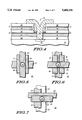
- FIGS. 1-3 illustrate, in cross-sectional form, a method for forming an interconnection structure in accordance with the present invention
- FIG. 4 illustrates, in cross-sectional form, an alternative interconnection structure
- FIG. 5 illustrates in a top perspective view a structure which is analogous to the cross-section of FIG. 3;
- FIG. 6 illustrates in a top perspective view another structure which is analogous to the cross-section of FIG. 3;
- FIG. 7 illustrates in a top perspective view a structure which is analogous to the cross-section of FIG. 4;
- FIGS. 8-9 illustrate, in cross-sectional form, another method for forming an interconnection structure in accordance with the present invention.
- FIGS. 10-14 each illustrate, in cross-sectional form, alternative interconnection structures which are formed via the structure illustrated in FIG. 8;
- FIGS. 15-17 illustrate, in cross-sectional form, yet another interconnection method which is in accordance with the present invention.
- Described herein is a contact and/or interconnection strategy which allows for the formation of a fully self-aligned contact and/or interconnect.
- the contact and/or interconnect hereafter referred to primarily as one of either a contact or an interconnect, allows for increased yield, increased process windows, reduced capacitive coupling between conductive layers, improved lifetime reliability, decreased integrated circuit surface area (i.e. more dense circuits), improved flexibility and improved functionality of conductive layers when compared to conventional methods of contacting.
- selective contacts between multiple layers may be formed.
- three conductive layers such as a diffusion, a second conductive layer, and a fourth conductive layer may be connected in a single self-aligned contact hole, fully self-aligned, with minimal surface area, and will have all of the advantages and flexibility discussed above and herein.
- FIG. 1 Illustrated in FIG. 1 is structure suitable for formation of an interconnection structure.
- a substrate 10 is provided.
- Substrate 10 preferably has a top planar surface prior to semiconductor processing.
- the substrate 10 is formed having a conductivity type which is one of either a P type conductivity or an N type conductivity if the substrate 10 is silicon-based.
- Substrate 10 may be made of silicon, gallium arsenide, silicon on insulator (SOI) structures, epitaxial formations, germanium, germanium silicon, polysilicon, amorphous silicon, and/or like substrate, semiconductive, or conductive materials.
- the substrate 10 is made of single-crystalline silicon, and is usually doped with boron, phosphorus, or arsenic atoms.
- Layer 12 may be a dielectric layer or layer 12 may be a plurality of device layers.
- Device layers are defined as being any conductive, semiconductive, dielectric layer, or similar layer which may be formed on or within the integrated circuit substrate 10.
- Device layers may be used to form devices such as transistors, diodes, capacitors, and the like.
- Layer 12 is used to illustrate that the interconnection structures presented herein may be positioned directly over the substrate 10, may be positioned overlying several layers of material, or may be positioned over one or more active devices.
- Conductive layer 14 is formed overlying the layer 12.
- Conductive layer 14 may be any known conductive layer, such as metal, metal alloys, epitaxial formations, and the like, but is preferably either N-doped or P-doped polysilicon. If conductive layer 14 is a polysilicon layer, a salicided or silicided layer 15 is optionally formed over a top portion of the conductive layer 14 to improve polysilicon conductivity.
- the silicided layer 15 and other silicided layers discussed herein may be formed via tungsten, platinum, titanium, cobalt, or like metallic elements.
- a dielectric layer 16 is formed overlying the silicided layer 15.
- Dielectric layer 16 is formed overlying the conductive layer 14 if the silicided layer 15 is not formed.
- the dielectric layers which are discussed herein may be wet or dry silicon dioxide (SiO 2 ), silicon nitride, tetraethylorthosilicate (TEOS) based oxides, borophospho-silicate-glass (BPSG), phospho-silicate-glass (PSG), boro-silicate-glass (BSG), oxide-nitride-oxide (ONO), oxynitride materials, plasma enhanced silicon nitride (P--SiN x ), a spin on glass (SOG), and/or like dielectric materials or composite dielectric films.
- Dielectric layer 16 is preferably a TEOS-based oxide layer.
- a conductive layer 18 is formed overlying the dielectric layer 16.
- the conductive layer 18 is similar to conductive layer 14 and is preferably a polysilicon layer. Other known conductive or semiconductive layers may be used for conductive layer 18.
- a salicided or silicided layer 17 is formed overlying the conductive layer 18.
- Silicided layer 17 is optional and is similar to silicided layer 15.
- a dielectric layer 20 is formed overlying the silicided layer 17. If the silicided layer 17 is not formed, the dielectric layer 20 is formed overlying the conductive layer 18.
- Dielectric layer 20 is preferably a TEOS based oxide.
- an opening 19 is formed sequentially through the layers 20, 17, 18, and 16.
- a masking layer such as photoresist, is formed overlying the dielectric layer 20.
- the masking layer (not illustrated) is exposed to light or like radiation and developed to form an opening (not illustrated) in the masking layer.
- This opening in the masking layer is used to define the geometry of the opening 19. In most cases, the opening 19 will be less than one micron in diameter.
- oxides may be etched using, for example, a CHF 3 and O 2 plasma or a C 2 F 6 plasma.
- Polysilicon may be etched using an HBr and Cl 2 plasma or a CF 4 /oxygen environment.
- Silicided layers may be etched via a chlorine HBr ambient. Any of the above stated plasma environments may contain one or more inert carrier gases such as Ar, H 2 , He, N 2 , or a like inert carrier gas.
- dielectric layer 20 is reactive ion etched (RIE) or etched in a like manner.
- Both the silicided layer 17 and the conductive layer 18 are preferably etched in an isotropic manner or in a two step RIE/isotropic manner to form a recessed sidewall portion 19a of the opening 19.
- An etch process using an SF 6 /oxygen plasma may be used to simultaneously etch both a silicide layer and a polysilicon layer although a two step process results in a more reliable recessed sidewall profile.
- the silicided layer 17 is etched in a first chemistry and the conductive layer 18 is etched in a second chemistry in a preferred form.
- Dielectric layer 16 is RIE etched wherein the dielectric layer 20 and the overlying masking layer (not illustrated) are used to ensure that the etching of dielectric layer 16 does not form a recessed sidewall as illustrated.
- the opening 19 is etched in a selective manner so that the opening 19 exposes but does not completely remove silicided layer 15 and conductive layer 14.
- etch processes involving several etch chemistries and involving the etching of several different material may be "clustered" in a single etch system under one vacuum ambient environment.
- Many different types of etches may be performed in this manner.
- a single etch system may have two equipment chambers which are each equipped for isotropic etching and two other chambers which are equipped for anisotropic etching. This system may be used to perform "cluster"etching with improved throughput and improved device quality. Less processing time and fewer exposures to different etch equipment systems usually results in less wafer contamination.
- a sidewall dielectric referred to as sidewall spacer 22 is formed adjacent the recessed sidewall portion 19a.
- Sidewall spacer 22 is formed as an oxide material, a nitride material, or a like insulator.
- sidewall spacer 22 is a furnace TEOS or a low pressure chemical vapor deposition (LPCVD) silicon nitride layer.
- LPCVD low pressure chemical vapor deposition
- the spacer 22 may not entirely form in the recessed sidewall portion 19a. If this phenomenon is a problem, a brief sidewall oxidation of the sidewall of the conductive layer 18 may be performed to form a sidewall oxidation layer (not illustrated). Once this sidewall oxidation step has partially or totally filled the recessed sidewall portion 19a, the spacer may be formed adjacent the sidewall oxidation layer (not illustrated). It is important to note that the phenomenon of not entirely filling the recessed sidewall portion 19a has not been observed experimentally when using furnace TEOS or LPCVD silicon nitride.
- a conductive layer 24 is formed within the opening 19, adjacent the spacer 22, and electrically contacting one or both of the silicided layer 15 and the conductive layer 14.
- An interconnection between the conductive layer 24 and the conductive layer 14 has been formed wherein conductive layer 18 is isolated via the spacer 22.
- the conductive layer 24 is a polysilicon layer which is optionally silicided. It is important to note that the conductive layer 24, as well as other conductive layers presented herein are not limited to polysilicon but may be made of metal, metal alloys, silicides, salicides, semiconductive material, and other like conductive and/or semiconductive formations.
- the interconnect structure illustrated in FIG. 3 has several advantages over the prior art.
- the contact opening 19 illustrated in FIG. 3 is illustrated as having an ideal vertical sidewall (i.e. 90° ). This vertical sidewall is said to have a 90° contact profile.
- contact profiles may vary from retrograded (i.e. greater than 90° ) to roughly 60° in profile from contact to contact, die to die, and wafer to wafer within a semiconductor wafer lot.
- Sidewall spacers formed adjacent contact sidewalls which have profiles less than 85° were experimentally found to be thin and unreliable. These thin spacers increase capacitive coupling between conductive layers, increase the tendency for electrical short circuits, reduce wafer lot yield, and reduce integrated circuit lifetime reliability.
- the contact of FIG. 3 has reduced capacitive coupling between conductive layer 18 and conductive layer 24, improved yield, improved integrated circuit lifetime, and reduced tendency towards electrical short circuiting. Furthermore, the contact of FIG. 3 is fully self-aligned and therefore has a small surface area, reduced tolerance limitations, and reduced reliance on lithographic alignment.
- sidewall isolation has been formed in the prior art by using sidewall oxidation techniques.
- Sidewall oxidation techniques or thermal oxidation of sidewalls alone may be feasible for some applications but not all.
- sidewall oxides will either not form or will not be of a good quality when formed from a silicided layer, a polysilicon layer, or a metal layer. Therefore, if a sidewall oxide is formed adjacent silicided layer 17, or if a metallic material is used for conductive layer 18, the sidewall oxidation is either impossible to perform or not reliable due to the fact that oxide growth adjacent these materials are of a poor quality.
- thermal oxide growth on a polysilicon layer is possible but this oxide is inferior in isolation capability and leakage current when compared to an LPCVD nitride spacer or a furnace TEOS spacer. Therefore, the structure illustrated in FIG. 3 is superior to the prior art interconnection structures in many ways.
- the conductive layers which are isolated from the contact are not limited in functionality or position in FIG. 3.
- the conductive layer 18 is in some cases required to be positioned away from the contact opening 19 to avoid electrical short circuiting to conductive layer 24. This positioning is determined by lithographic alignment tolerances and may limit conductive layer 18 by separations/distances which measure on the order of a micron to one tenth of a micron.
- the known tolerance-determined positioning limitation of the prior art interconnection conductive layers may limit the functionality, complexity, performance, surface area, and/or layout freedom associated with a conductive layer.
- the conductive layer 18 is a ground voltage plane
- the reduction in surface area which results from the noted tolerance positioning limitations will increase the resistance of the ground voltage plane or increase ground interconnect wiring. Increased ground resistance and increased ground routing is not desirable. Also conductive layer 18 may not be capable of being easily routed to another integrated circuit location due to an intervening contact hole.
- conductive plug and conductive planarized interconnect technologies exist.
- barrier regions or peripheral regions i.e. titanium nitride, silicides, titanium/tungsten, or the like
- conductive plug materials i.e. tungsten, other refractory metals, metal composites, metals, silicides or salicides, or the like. Any one of these known plugs may be used as conductive layer 24 to improve interconnection performance.
- FIG. 4 illustrates another interconnection structure.
- the structure of FIG. 4 may be manufactured by first performing the steps illustrated and discussed in reference to FIGS. 1-2. After the structure of FIG. 2 is achieved, the spacer 22 is formed in a manner similar to FIG. 3. After the spacer 22 is formed, an etch process is used to etch through the layers 15, 14, and 12 to expose a portion of the surface of the substrate 10. The etch is self-aligned to opening 19 via the spacer 22. An optional diffusion 25 is either previously formed in a non-self-aligned conventional manner prior to formation of the opening 19, or is formed self-aligned to contact opening 19 after the substrate 10 is exposed. The diffusion 25 is a phosphorus, arsenic, and/or boron doped portion of the substrate 10. The opening in conductive layer 14 forms a sidewall of conductive layer 14.
- the conductive layer 24 is formed within the opening 19 and electrically connects conductive layer 24 to conductive layer 14.
- One of either the diffusion 25 or the substrate 10 is electrically contacted via the conductive layer 24.
- a substrate contact or a contact to an electrode of a transistor may be formed in this manner.
- FIGS. 5-7 illustrate several top perspective views of structures which are analogous to one of either FIG. 3 or FIG. 4. Elements in FIGS. 5-7 which are analogous to elements in FIGS. 1-4 are identically labeled.
- the contact opening 19 forms a hole through a central portion of conductive layer 18, and exposes a central portion of conducive layer 14.
- the spacer 22 is formed around a peripheral sidewall of the opening 19.
- Conductive layer 24 is formed within the contact opening 19 to electrically connect conductive layer 24 to conductive layer 14.
- FIG. 6 illustrates the contact opening 19.
- the contact opening 19 intersects a peripheral portion of a first portion of conductive layer 18 and intersects a peripheral portion of a second portion of conductive layer 18.
- Contact opening 19 exposes a central portion of conductive layer 14.
- Spacer 22 is formed and conductive layer 24 is formed to complete the electrical contact.
- Conductive layer 18 is isolated from the connection via the spacer 22.
- FIG. 7 also illustrates the contact opening 19.
- Contact opening 19 intersects a peripheral portion of conductive layer 18, intersects a peripheral portion of conductive layer 14, and exposes a portion of diffusion 25.
- the spacer 22 is formed to isolate selective conductive layers exposed on a sidewall via the opening 19.
- the conductive layer 24 is formed to complete the contact.
- FIGS. 5-7 illustrate only three of several top perspective design possibilities. Other permutations of top down contact configurations exist using intersected lines, spacer isolated lines, and exposed portions of conductive layers. By using the teachings of FIG. 1-7, other interconnection structures may be readily derived.
- FIG. 8 illustrates a structure suitable for formation of an interconnection structure.
- the substrate 10 is illustrated along with the layer 12.
- Substrate 10 and layer 12 are analogous to the substrate 10 and layer 12 of FIG. 1.
- a conductive layer 26 is formed overlying the layer 12.
- a dielectric layer 28 is formed overlying the conductive layer 26.
- a conductive layer 30 is formed overlying dielectric layer 28.
- a dielectric layer 32 is formed overlying conductive layer 30.
- a conductive layer 34 is formed overlying dielectric layer 32.
- a dielectric layer 36 is formed overlying the conductive layer 34.
- the dielectric layers 28, 32, and 36 may be any known insulator or any dielectric material discussed herein.
- Each of the conductive layers 26, 30, and 34 is either a metal, a silicon-based material, or any known conductive or semiconductive material. If a silicon-based conductive material is used to form one or more of the conductive layers 26, 30, and 34, the silicon-based conductive material (e.g. polysilicon, epitaxial silicon, etc.) is optionally silicided or salicided.
- layers 28, 30, 32, 34, and 36 are etched as described herein to form an opening 37.
- Furnace TEOS, LPCVD nitride, or a like conformal dielectric is deposited and RIE etched to form a spacer 35.
- the spacer 35 is vertically recessed downward from a sidewall of conductive layer 34 via an RIE over-etch step.
- the RIE over-etch step exposes the sidewall of conductive layer 34 while isolating conductive layer 30 via spacer 35.
- a conductive layer 38 is formed within opening 37 and electrically connects conductive layer 38, conductive layer 34, and conductive layer 26.
- the isotropic recessed etch process discussed herein is used to laterally recess the sidewalls of conductive layer 30 prior to the formation of spacer 35. This lateral recessing is selective to the adjacent dielectric layers 28, 32, and 36.
- Methods of making sidewall masks are known. These sidewall masks may be used to protect sidewall regions from isotropic etch steps.
- FIG. 10 illustrates another structure which may be formed via the structure of FIG. 8.
- layers 28, 30, 32, 34, and 36 are etched as in FIG. 9 to form the opening 37.
- a spacer 39 which is similar to spacer 25 of FIG. 9 is formed.
- the spacer 39 is used to etch a self-aligned hole through layers 26 and 12 to expose the substrate 10.
- a diffusion 40 is optionally formed within the substrate as taught herein.
- the conductive layer 38 is formed to contact conductive layers 38, 34, and 26 to the diffusion 40 or the substrate 10.
- Conductive layer 30 is isolated from the contact via spacer 39 and a lateral recessing step.
- FIG. 11 illustrates another interconnection structure.
- the structure of FIG. 8 is etched to form the opening 37 through layers 32, 34, and 36.
- a spacer 41 is formed to isolate the conductive layer 34.
- the layers 28 and 30 are etched self-aligned to the spacer 41.
- the layer 34 is isotropically recessed as discussed herein for improved isolation and reliability.
- the conductive layer 38 electrically connects together conductive layers 38, 30, and 26. It should be noted that a contact to the substrate 10 or diffusion contact (not illustrated) may be made via the structure of FIG. 11 by etching through layers 26 and 12 as taught herein.
- FIG. 12 illustrates yet another interconnection structure.
- the structure of FIG. 8 is etched to form the opening 37 through layers 28, 30, 32, 34, and 36.
- the conductive layers 30 and 34 may both be isotropically recessed or be individually isotropically etched as taught herein to improve isolation and reliability.
- a spacer 42 is formed to isolate the conductive layer 34.
- the conductive layer 38 electrically connects together conductive layers 38 and 26 while isolating, in a self-aligned manner and in a small surface area, conductive layers 30 and 34 from the interconnection.
- FIG. 13 illustrates yet another interconnection structure.
- the structure of FIG. 8 is etched to form the opening 37 through layers 12, 26, 28, 30, 32, 34, and 36.
- the conductive layer 26 may be isotropically recessed as taught herein to improve isolation and reliability.
- the conductive layer 38 electrically connects together conductive layers 30, 34, and 38.
- the interconnect contacts to an optional diffusion 44. The interconnect connects to the substrate 10 if the diffusion 44 is not formed.
- FIG. 14 illustrates yet another interconnection structure.
- the structure of FIG. 8 is etched to form the opening 37 through layers 12, 26, 28, 30, 32, 34, and 36.
- the conductive layers 26, 30, and/or 34 may be isotropically recessed via one or more selective isotropic etch steps as taught herein to improved isolation and reliability.
- a spacer 48 is formed to isolate conductive layers 26, 30, and 34 from the interconnection.
- the conductive layer 38 electrically contacts to a diffusion 46 or the substrate 10 to form an interconnect.
- FIGS. 1-14 do not exhaustively illustrate all combinations of interconnect structures which may result using the techniques taught herein. It should be understood from FIGS. 1-14 that other interconnect structures having N conductive layers, wherein N is a positive integer, may be formed.
- the N conductive layers may be isolated by dielectric layers as illustrated herein.
- the N conductive layers may be selectively connected as taught herein via sidewall recess processing, etch processing which is used to form openings, deposition techniques, and spacer formation.
- a typical number for N may be any value ranging from two through eight.
- conductive layers may be formed wherein the six conductive layers are rank-ordered with layer one being a bottom layer and layer six being a top layer.
- Layer six may be connected to layer two, connected to layer one, and optionally connected to a diffusion by forming an opening as taught herein, defining a spacer as taught herein, and depositing a seventh conductive layer to form the interconnection.
- the layers three through five are isolated from the contact via the spacer.
- a spacer formed within the contact or interconnect may not be desirable.
- the spacer reduces a radius of the contact or interconnect thereby increasing contact resistance and adversely affecting contact reliability (i.e. small features may not be completely filled by some conductive materials). Therefore, it is desirable to have a contact having all of the advantages described herein wherein a sidewall spacer is not formed.
- FIGS. 15-17 illustrate a method for forming an interconnection structure wherein isolation is achieved selectively between conductive layers and no spacer is utilized.
- the structure of FIG. 2 is illustrated having a dielectric layer 22a, which is formed by LPCVD nitride, furnace TEOS, or a like dielectric material. All elements in FIG. 15 which are analogous to elements in FIG. 2 are identically labeled.
- the dielectric layer 22a of FIG. 15 is RIE etched to form the spacer 22.
- the spacer 22 is RIE over-etched to form a region which is now referred to as sidewall oxide region 22.
- Sidewall oxide region 22 has less defects and has a leakage current which is less than a thermally grown sidewall oxide.
- a quality sidewall oxide cannot be grown on a sidewall of a silicide layer whereas sidewall oxide region 22 may be formed adjacent silicided layers. If the contact profile of opening 19 is less than 85° , a spacer may not form on the sidewall and a spacer RIE over-etch step, as illustrated in FIGS. 16-17, may not be required to form sidewall oxide region 22.
- FIGS. 15-17 may be applied to any embodiment illustrated herein or any inventive method or structure taught herein.
- the structure illustrated in FIG. 17 has an improved contact resistance, improved isolation due to a higher-quality sidewall dielectric material, and improved contact reliability over the prior art.
- N conductive layers may be used to form self-aligned interconnects via the methods taught herein.
- the contacts discussed herein are useful for memory applications, such as static random access memories (SRAMs) and may be used for vertical integration or vertical logic. Spacers and grown sidewall oxides may be combined to improve isolation between conductive layers (i.e. two different oxide materials may be used, one grown and one deposited).
Abstract
Description
Claims (18)
Priority Applications (1)
| Application Number | Priority Date | Filing Date | Title |
|---|---|---|---|
| US08/286,592 US5408130A (en) | 1992-08-31 | 1994-08-05 | Interconnection structure for conductive layers |
Applications Claiming Priority (3)
| Application Number | Priority Date | Filing Date | Title |
|---|---|---|---|
| US07/937,025 US5262352A (en) | 1992-08-31 | 1992-08-31 | Method for forming an interconnection structure for conductive layers |
| US9892593A | 1993-07-29 | 1993-07-29 | |
| US08/286,592 US5408130A (en) | 1992-08-31 | 1994-08-05 | Interconnection structure for conductive layers |
Related Parent Applications (1)
| Application Number | Title | Priority Date | Filing Date |
|---|---|---|---|
| US9892593A Continuation | 1992-08-31 | 1993-07-29 |
Publications (1)
| Publication Number | Publication Date |
|---|---|
| US5408130A true US5408130A (en) | 1995-04-18 |
Family
ID=25469378
Family Applications (2)
| Application Number | Title | Priority Date | Filing Date |
|---|---|---|---|
| US07/937,025 Expired - Lifetime US5262352A (en) | 1992-08-31 | 1992-08-31 | Method for forming an interconnection structure for conductive layers |
| US08/286,592 Expired - Lifetime US5408130A (en) | 1992-08-31 | 1994-08-05 | Interconnection structure for conductive layers |
Family Applications Before (1)
| Application Number | Title | Priority Date | Filing Date |
|---|---|---|---|
| US07/937,025 Expired - Lifetime US5262352A (en) | 1992-08-31 | 1992-08-31 | Method for forming an interconnection structure for conductive layers |
Country Status (1)
| Country | Link |
|---|---|
| US (2) | US5262352A (en) |
Cited By (49)
| Publication number | Priority date | Publication date | Assignee | Title |
|---|---|---|---|---|
| US5470790A (en) * | 1994-10-17 | 1995-11-28 | Intel Corporation | Via hole profile and method of fabrication |
| US5589713A (en) * | 1992-01-23 | 1996-12-31 | Samsung Electronics Co., Ltd. | Semiconductor device having an improved wiring layer |
| US5599749A (en) * | 1994-10-21 | 1997-02-04 | Yamaha Corporation | Manufacture of micro electron emitter |
| US5616960A (en) * | 1993-07-05 | 1997-04-01 | Sony Corporation | Multilayered interconnection substrate having a resin wall formed on side surfaces of a contact hole |
| US5623160A (en) * | 1995-09-14 | 1997-04-22 | Liberkowski; Janusz B. | Signal-routing or interconnect substrate, structure and apparatus |
| US5633197A (en) * | 1994-05-11 | 1997-05-27 | United Microelectronics Corporation | Metallization to improve electromigration resistance by etching concavo-concave opening |
| US5683930A (en) * | 1995-12-06 | 1997-11-04 | Micron Technology Inc. | SRAM cell employing substantially vertically elongated pull-up resistors and methods of making, and resistor constructions and methods of making |
| US5705409A (en) * | 1995-09-28 | 1998-01-06 | Motorola Inc. | Method for forming trench transistor structure |
| US5717240A (en) * | 1993-12-29 | 1998-02-10 | Mitsubishi Denki Kabushiki Kaisha | Static semiconductor memory device |
| US5757612A (en) * | 1996-04-23 | 1998-05-26 | International Business Machines Corporation | Structure and fabrication method for non-planar memory elements |
| US5795208A (en) * | 1994-10-11 | 1998-08-18 | Yamaha Corporation | Manufacture of electron emitter by replica technique |
| US5847460A (en) * | 1995-12-19 | 1998-12-08 | Stmicroelectronics, Inc. | Submicron contacts and vias in an integrated circuit |
| US5851923A (en) * | 1996-01-18 | 1998-12-22 | Micron Technology, Inc. | Integrated circuit and method for forming and integrated circuit |
| US5869391A (en) * | 1996-08-20 | 1999-02-09 | Micron Technology, Inc. | Semiconductor method of making electrical connection between an electrically conductive line and a node location, and integrated circuitry |
| US5879971A (en) * | 1995-09-28 | 1999-03-09 | Motorola Inc. | Trench random access memory cell and method of formation |
| US5880033A (en) * | 1996-06-17 | 1999-03-09 | Applied Materials, Inc. | Method for etching metal silicide with high selectivity to polysilicon |
| US5883436A (en) * | 1994-11-18 | 1999-03-16 | Intel Corporation | Contact and via fabrication technologies |
| US5886382A (en) * | 1997-07-18 | 1999-03-23 | Motorola, Inc. | Trench transistor structure comprising at least two vertical transistors |
| US5894169A (en) * | 1995-04-05 | 1999-04-13 | International Business Machines Corporation | Low-leakage borderless contacts to doped regions |
| US5965938A (en) * | 1996-03-25 | 1999-10-12 | Taiwan Semiconductor Manufacturing Company, Ltd. | Integrated two-tiered via-plug to improve metal lithography # 4 |
| US5972757A (en) * | 1995-01-31 | 1999-10-26 | Fujitsu Limited | Method of forming a self aligned through-hole on a diffused layer |
| US5976985A (en) * | 1997-08-14 | 1999-11-02 | Micron Technology, Inc. | Processing methods of forming contact openings and integrated circuitry |
| US5987744A (en) | 1996-04-10 | 1999-11-23 | Prolinx Labs Corporation | Method for supporting one or more electronic components |
| US6008139A (en) * | 1996-06-17 | 1999-12-28 | Applied Materials Inc. | Method of etching polycide structures |
| US6033985A (en) * | 1998-06-30 | 2000-03-07 | National Science Council Of Republic Of China | Contact process interconnect poly-crystal silicon layer in thin film SRAM |
| US6090698A (en) * | 1999-07-23 | 2000-07-18 | United Microelectronics Corp | Fabrication method for an insulation structure having a low dielectric constant |
| US6117733A (en) * | 1998-05-27 | 2000-09-12 | Taiwan Semiconductor Manufacturing Company | Poly tip formation and self-align source process for split-gate flash cell |
| US6169010B1 (en) * | 1999-01-26 | 2001-01-02 | Lucent Technologies Inc. | Method for making integrated circuit capacitor including anchored plug |
| US6171964B1 (en) * | 1996-02-02 | 2001-01-09 | Micron Technology, Inc. | Method of forming a conductive spacer in a via |
| US6242321B1 (en) | 1996-04-23 | 2001-06-05 | International Business Machines Corporation | Structure and fabrication method for non-planar memory elements |
| US6259131B1 (en) | 1998-05-27 | 2001-07-10 | Taiwan Semiconductor Manufacturing Company | Poly tip and self aligned source for split-gate flash cell |
| US6274936B1 (en) * | 1995-07-10 | 2001-08-14 | Micron Technology, Inc. | Method for forming a contact during the formation of a semiconductor device |
| US6303438B1 (en) * | 1998-02-02 | 2001-10-16 | Matsushita Electric Industrial Co., Ltd. | Method for manufacturing a nonvolatile semiconductor memory device having increased hot electron injection efficiency |
| EP1030359A3 (en) * | 1999-02-19 | 2002-08-21 | Micronas GmbH | Layered structure and method of making it |
| US20020130380A1 (en) * | 2001-03-16 | 2002-09-19 | Theil Jeremy A. | Simplified upper electrode contact structure for PIN diode active pixel sensor |
| US6577005B1 (en) * | 1997-11-27 | 2003-06-10 | Kabushiki Kaishia Toshiba | Fine protuberance structure and method of production thereof |
| US20030134470A1 (en) * | 1990-03-08 | 2003-07-17 | Fujitsu Limited | Layer structure having contact hole, fin-shaped capacitor using the layer structure, method of producing the fin-shaped capacitor, and dynamic random access memory having the fin-shaped capacitor |
| US20040197976A1 (en) * | 2002-12-30 | 2004-10-07 | Rodgers John C. | Method for manufacturing sidewall contacts for a chalcogenide memory device |
| US6903411B1 (en) * | 2000-08-25 | 2005-06-07 | Agere Systems Inc. | Architecture for circuit connection of a vertical transistor |
| US20050242870A1 (en) * | 2004-03-30 | 2005-11-03 | Hideyuki Aota | Reference voltage generating circuit |
| US20060160351A1 (en) * | 2000-11-01 | 2006-07-20 | Samsung Electronics, Co., Ltd. | Metal interconnect layer of semiconductor device and method for forming a metal interconnect layer |
| CN1329973C (en) * | 2004-02-05 | 2007-08-01 | 台湾积体电路制造股份有限公司 | Interconnect structure , method for its fabricating and IC assembly |
| US20070216015A1 (en) * | 2004-01-30 | 2007-09-20 | Koninklijke Philips Electronics N.V. | Integrated Circuit Chip With Electrostatic Discharge Protection Device |
| US20080239610A1 (en) * | 2006-07-19 | 2008-10-02 | Ho-Chieh Yu | Chip scale gas discharge protective device and fabrication method of the same |
| EP2008300A2 (en) * | 2006-04-04 | 2008-12-31 | International Business Machines Corporation | Self-aligned body contact for an semiconductor-on-insulator trench device and method of fabricating same |
| US20100244255A1 (en) * | 2009-03-26 | 2010-09-30 | Samsung Electronics Co., Ltd. | Wiring structures |
| DE102009043329A1 (en) * | 2009-09-30 | 2011-03-31 | GLOBALFOUNDRIES Dresden Module One Ltd. Liability Company & Co. KG | Clamping technology in a contact plane of semiconductor devices by means of strained conductive layers and an insulating spacer |
| US20110183516A1 (en) * | 2009-03-26 | 2011-07-28 | Samsung Electronics Co., Ltd. | Methods of forming wiring structures |
| CN110021603A (en) * | 2019-04-11 | 2019-07-16 | 德淮半导体有限公司 | Semiconductor structure and forming method thereof |
Families Citing this family (51)
| Publication number | Priority date | Publication date | Assignee | Title |
|---|---|---|---|---|
| JP3166221B2 (en) * | 1991-07-23 | 2001-05-14 | 日本電気株式会社 | Semiconductor device and manufacturing method thereof |
| KR950011556B1 (en) * | 1992-07-03 | 1995-10-06 | 현대전자산업주식회사 | Ohmic contact forming method of semiconductor device |
| KR0136569B1 (en) * | 1992-10-24 | 1998-04-29 | 김주용 | Fabrication method of contact hole in semiconductor device |
| DE4239075C1 (en) * | 1992-11-20 | 1994-04-07 | Itt Ind Gmbh Deutsche | Process for the global planarization of surfaces of integrated semiconductor circuits |
| KR950011983B1 (en) * | 1992-11-23 | 1995-10-13 | 삼성전자주식회사 | Fabricating method of semiconductor device |
| JP2830658B2 (en) * | 1992-11-25 | 1998-12-02 | 日本電気株式会社 | Fine metal wiring forming method |
| JP3158749B2 (en) * | 1992-12-16 | 2001-04-23 | ヤマハ株式会社 | Semiconductor device |
| US5439848A (en) * | 1992-12-30 | 1995-08-08 | Sharp Microelectronics Technology, Inc. | Method for fabricating a self-aligned multi-level interconnect |
| US5357397A (en) * | 1993-03-15 | 1994-10-18 | Hewlett-Packard Company | Electric field emitter device for electrostatic discharge protection of integrated circuits |
| US6690044B1 (en) * | 1993-03-19 | 2004-02-10 | Micron Technology, Inc. | Approach to avoid buckling BPSG by using an intermediate barrier layer |
| DE4309611A1 (en) * | 1993-03-24 | 1994-09-29 | Siemens Ag | Manufacturing process for a contact hole |
| US5650655A (en) * | 1994-04-28 | 1997-07-22 | Micron Technology, Inc. | Integrated circuitry having electrical interconnects |
| KR0136684B1 (en) * | 1993-06-01 | 1998-04-29 | Matsushita Electric Ind Co Ltd | Semiconductor device and manufacture thereof |
| KR0161731B1 (en) * | 1994-10-28 | 1999-02-01 | 김주용 | Method of fabricating fine contact of semiconductor device |
| US6140705A (en) * | 1995-01-03 | 2000-10-31 | Texas Instruments Incorporated | Self-aligned contact through a conducting layer |
| US5753375A (en) * | 1995-01-05 | 1998-05-19 | Santa Barbara Research Center | Microelectronic device having dark mirror coating with vias therethrough |
| JP3160198B2 (en) * | 1995-02-08 | 2001-04-23 | インターナショナル・ビジネス・マシーンズ・コーポレ−ション | Semiconductor substrate on which decoupling capacitor is formed and method of manufacturing the same |
| US5684331A (en) * | 1995-06-07 | 1997-11-04 | Lg Semicon Co., Ltd. | Multilayered interconnection of semiconductor device |
| SG54548A1 (en) * | 1996-08-28 | 1998-11-16 | Texas Instruments Inc | Contact formation for a semiconductor device |
| US6037246A (en) | 1996-09-17 | 2000-03-14 | Motorola Inc. | Method of making a contact structure |
| US5739066A (en) | 1996-09-17 | 1998-04-14 | Micron Technology, Inc. | Semiconductor processing methods of forming a conductive gate and line |
| JPH1098100A (en) * | 1996-09-20 | 1998-04-14 | Nec Corp | Contact hole/through-hole formation method |
| KR100190105B1 (en) * | 1996-10-24 | 1999-07-01 | 윤종용 | Manufacturing method of gate electrode and the structure of the same |
| US20020137890A1 (en) * | 1997-03-31 | 2002-09-26 | Genentech, Inc. | Secreted and transmembrane polypeptides and nucleic acids encoding the same |
| US6054340A (en) | 1997-06-06 | 2000-04-25 | Motorola, Inc. | Method for forming a cavity capable of accessing deep fuse structures and device containing the same |
| US5895264A (en) * | 1997-07-30 | 1999-04-20 | Chartered Semiconductor Manufacturing Ltd. | Method for forming stacked polysilicon |
| US6008123A (en) * | 1997-11-04 | 1999-12-28 | Lucent Technologies Inc. | Method for using a hardmask to form an opening in a semiconductor substrate |
| US6040241A (en) * | 1998-02-11 | 2000-03-21 | United Microelectronics Corp. | Method of avoiding sidewall residue in forming connections |
| US6140217A (en) * | 1998-07-16 | 2000-10-31 | International Business Machines Corporation | Technique for extending the limits of photolithography |
| US6143611A (en) * | 1998-07-30 | 2000-11-07 | Micron Technology, Inc. | Semiconductor processing methods, methods of forming electronic components, and transistors |
| US6448140B1 (en) * | 1999-02-08 | 2002-09-10 | Taiwan Semiconductor Manufacturing Company | Laterally recessed tungsten silicide gate structure used with a self-aligned contact structure including a straight walled sidewall spacer while filling recess |
| US7482278B1 (en) | 1999-02-11 | 2009-01-27 | Taiwan Semiconductor Manufacturing Co., Ltd. | Key-hole free process for high aspect ratio gap filling with reentrant spacer |
| US6153517A (en) * | 1999-03-12 | 2000-11-28 | Taiwan Semiconductor Manufacturing Company | Low resistance poly landing pad |
| KR100295061B1 (en) | 1999-03-29 | 2001-07-12 | 윤종용 | Semiconductor device having chamfered silicide layer and method for manufacturing the same |
| US6136695A (en) * | 1999-08-04 | 2000-10-24 | Taiwan Semiconductor Manufacturing Company | Method for fabricating a self-aligned contact |
| KR100297738B1 (en) | 1999-10-07 | 2001-11-02 | 윤종용 | Method for manufacturing semiconductor device having chamfered metal silicide layer |
| US6566236B1 (en) | 2000-04-26 | 2003-05-20 | Integrated Device Technology, Inc. | Gate structures with increased etch margin for self-aligned contact and the method of forming the same |
| KR100343284B1 (en) * | 2000-06-23 | 2002-07-15 | 윤종용 | Bonding pad structure in semiconductor device and fabrication method thereof |
| US6458646B1 (en) | 2000-06-30 | 2002-10-01 | International Business Machines Corporation | Asymmetric gates for high density DRAM |
| KR100383325B1 (en) * | 2001-01-19 | 2003-05-12 | 삼성전자주식회사 | Wiring of semiconductor device for forming a self-aligned contact and Method of manufacturing the same |
| US6593192B2 (en) * | 2001-04-27 | 2003-07-15 | Micron Technology, Inc. | Method of forming a dual-gated semiconductor-on-insulator device |
| US6906129B2 (en) | 2003-09-05 | 2005-06-14 | Shin-Etsu Chemical Co., Ltd. | Polymer scale preventive agent |
| DE102006007331A1 (en) * | 2006-02-16 | 2007-08-23 | Infineon Technologies Ag | Multilayer capacitance arrangement e.g. metal-insulator-metal capacitance arrangement, for use in integrated circuit, has electrically conductive layer arranged over metallization layer, and dielectric layer arranged over conductive layer |
| JP2009037115A (en) * | 2007-08-03 | 2009-02-19 | Sony Corp | Semiconductor device, its manufacturing method, and display device |
| CN101874301B (en) * | 2007-11-27 | 2012-05-09 | Nxp股份有限公司 | Contact structure for an electronic circuit substrate and electronic circuit comprising said contact structure |
| US8476742B2 (en) * | 2008-02-28 | 2013-07-02 | Hewlett-Packard Development Company, L.P. | Fluid ejection device comprising substrate contact via |
| US7928577B2 (en) * | 2008-07-16 | 2011-04-19 | Micron Technology, Inc. | Interconnect structures for integration of multi-layered integrated circuit devices and methods for forming the same |
| US8735289B2 (en) * | 2010-11-29 | 2014-05-27 | Infineon Technologies Ag | Method of contacting a doping region in a semiconductor substrate |
| FR3030881A1 (en) * | 2014-12-22 | 2016-06-24 | Commissariat Energie Atomique | METHOD FOR MAKING AN INTEGRATED CIRCUIT IN THREE DIMENSIONS |
| US20190086809A1 (en) * | 2017-09-21 | 2019-03-21 | United Microelectronics Corp. | Method for fabricating semiconductor structure involving cleaning mask material |
| US11037874B2 (en) * | 2018-10-29 | 2021-06-15 | Intel Corporation | Plane-less voltage reference interconnects |
Citations (12)
| Publication number | Priority date | Publication date | Assignee | Title |
|---|---|---|---|---|
| US4656732A (en) * | 1984-09-26 | 1987-04-14 | Texas Instruments Incorporated | Integrated circuit fabrication process |
| US4700457A (en) * | 1985-03-29 | 1987-10-20 | Mitsubishi Denki Kabushiki Kaisha | Method of making multilayer capacitor memory device |
| US4872050A (en) * | 1988-03-15 | 1989-10-03 | Mitsubishi Denki Kabushiki Kaisha | Interconnection structure in semiconductor device and manufacturing method of the same |
| US4900695A (en) * | 1986-12-17 | 1990-02-13 | Hitachi, Ltd. | Semiconductor integrated circuit device and process for producing the same |
| US4924295A (en) * | 1986-11-28 | 1990-05-08 | Siemens Aktiengesellschaft | Integrated semi-conductor circuit comprising at least two metallization levels composed of aluminum or aluminum compounds and a method for the manufacture of same |
| US4977105A (en) * | 1988-03-15 | 1990-12-11 | Mitsubishi Denki Kabushiki Kaisha | Method for manufacturing interconnection structure in semiconductor device |
| US5045501A (en) * | 1986-08-25 | 1991-09-03 | Hughes Aircraft Company | Method of forming an integrated circuit structure with multiple common planes |
| US5051794A (en) * | 1988-07-05 | 1991-09-24 | Kabushiki Kaisha Toshiba | Non-volatile semiconductor memory device and method for manufacturing the same |
| US5091762A (en) * | 1988-07-05 | 1992-02-25 | Kabushiki Kaisha Toshiba | Semiconductor memory device with a 3-dimensional structure |
| US5100838A (en) * | 1990-10-04 | 1992-03-31 | Micron Technology, Inc. | Method for forming self-aligned conducting pillars in an (IC) fabrication process |
| US5116776A (en) * | 1989-11-30 | 1992-05-26 | Sgs-Thomson Microelectronics, Inc. | Method of making a stacked copacitor for dram cell |
| US5204286A (en) * | 1991-10-15 | 1993-04-20 | Micron Technology, Inc. | Method of making self-aligned contacts and vertical interconnects to integrated circuits |
-
1992
- 1992-08-31 US US07/937,025 patent/US5262352A/en not_active Expired - Lifetime
-
1994
- 1994-08-05 US US08/286,592 patent/US5408130A/en not_active Expired - Lifetime
Patent Citations (12)
| Publication number | Priority date | Publication date | Assignee | Title |
|---|---|---|---|---|
| US4656732A (en) * | 1984-09-26 | 1987-04-14 | Texas Instruments Incorporated | Integrated circuit fabrication process |
| US4700457A (en) * | 1985-03-29 | 1987-10-20 | Mitsubishi Denki Kabushiki Kaisha | Method of making multilayer capacitor memory device |
| US5045501A (en) * | 1986-08-25 | 1991-09-03 | Hughes Aircraft Company | Method of forming an integrated circuit structure with multiple common planes |
| US4924295A (en) * | 1986-11-28 | 1990-05-08 | Siemens Aktiengesellschaft | Integrated semi-conductor circuit comprising at least two metallization levels composed of aluminum or aluminum compounds and a method for the manufacture of same |
| US4900695A (en) * | 1986-12-17 | 1990-02-13 | Hitachi, Ltd. | Semiconductor integrated circuit device and process for producing the same |
| US4872050A (en) * | 1988-03-15 | 1989-10-03 | Mitsubishi Denki Kabushiki Kaisha | Interconnection structure in semiconductor device and manufacturing method of the same |
| US4977105A (en) * | 1988-03-15 | 1990-12-11 | Mitsubishi Denki Kabushiki Kaisha | Method for manufacturing interconnection structure in semiconductor device |
| US5051794A (en) * | 1988-07-05 | 1991-09-24 | Kabushiki Kaisha Toshiba | Non-volatile semiconductor memory device and method for manufacturing the same |
| US5091762A (en) * | 1988-07-05 | 1992-02-25 | Kabushiki Kaisha Toshiba | Semiconductor memory device with a 3-dimensional structure |
| US5116776A (en) * | 1989-11-30 | 1992-05-26 | Sgs-Thomson Microelectronics, Inc. | Method of making a stacked copacitor for dram cell |
| US5100838A (en) * | 1990-10-04 | 1992-03-31 | Micron Technology, Inc. | Method for forming self-aligned conducting pillars in an (IC) fabrication process |
| US5204286A (en) * | 1991-10-15 | 1993-04-20 | Micron Technology, Inc. | Method of making self-aligned contacts and vertical interconnects to integrated circuits |
Non-Patent Citations (2)
| Title |
|---|
| "A Split Wordline Cell for 16Mb SRAM Using Polysilicon Sidewall Contacts," by Itabashi et al., published via IEDM 1991, pp. 477-480. |
| A Split Wordline Cell for 16Mb SRAM Using Polysilicon Sidewall Contacts, by Itabashi et al., published via IEDM 1991, pp. 477 480. * |
Cited By (87)
| Publication number | Priority date | Publication date | Assignee | Title |
|---|---|---|---|---|
| US20030134470A1 (en) * | 1990-03-08 | 2003-07-17 | Fujitsu Limited | Layer structure having contact hole, fin-shaped capacitor using the layer structure, method of producing the fin-shaped capacitor, and dynamic random access memory having the fin-shaped capacitor |
| US5589713A (en) * | 1992-01-23 | 1996-12-31 | Samsung Electronics Co., Ltd. | Semiconductor device having an improved wiring layer |
| US5930676A (en) * | 1993-07-05 | 1999-07-27 | Sony Corporation | Multilayered interconnection substrate and process for fabricating the same |
| US5616960A (en) * | 1993-07-05 | 1997-04-01 | Sony Corporation | Multilayered interconnection substrate having a resin wall formed on side surfaces of a contact hole |
| US5717240A (en) * | 1993-12-29 | 1998-02-10 | Mitsubishi Denki Kabushiki Kaisha | Static semiconductor memory device |
| US5828134A (en) * | 1994-05-11 | 1998-10-27 | United Microelectronics Corporation | Metallization to improve electromigration resistance |
| US5633197A (en) * | 1994-05-11 | 1997-05-27 | United Microelectronics Corporation | Metallization to improve electromigration resistance by etching concavo-concave opening |
| US5795208A (en) * | 1994-10-11 | 1998-08-18 | Yamaha Corporation | Manufacture of electron emitter by replica technique |
| GB2308234A (en) * | 1994-10-17 | 1997-06-18 | Intel Corp | A novel via hole profile and method fabrication |
| WO1996012295A1 (en) * | 1994-10-17 | 1996-04-25 | Intel Corporation | A novel via hole profile and method of fabrication |
| GB2308234B (en) * | 1994-10-17 | 1999-04-14 | Intel Corp | A novel via hole profile and method fabrication |
| US5470790A (en) * | 1994-10-17 | 1995-11-28 | Intel Corporation | Via hole profile and method of fabrication |
| US5874358A (en) * | 1994-10-17 | 1999-02-23 | Intel Corporation | Via hole profile and method of fabrication |
| US5619071A (en) * | 1994-10-17 | 1997-04-08 | Intel Corporation | Anchored via connection |
| US5599749A (en) * | 1994-10-21 | 1997-02-04 | Yamaha Corporation | Manufacture of micro electron emitter |
| US5883436A (en) * | 1994-11-18 | 1999-03-16 | Intel Corporation | Contact and via fabrication technologies |
| US6495470B2 (en) | 1994-11-18 | 2002-12-17 | Intel Corporation | Contact and via fabrication technologies |
| US5972757A (en) * | 1995-01-31 | 1999-10-26 | Fujitsu Limited | Method of forming a self aligned through-hole on a diffused layer |
| US5894169A (en) * | 1995-04-05 | 1999-04-13 | International Business Machines Corporation | Low-leakage borderless contacts to doped regions |
| US6274936B1 (en) * | 1995-07-10 | 2001-08-14 | Micron Technology, Inc. | Method for forming a contact during the formation of a semiconductor device |
| US5691209A (en) * | 1995-09-14 | 1997-11-25 | Liberkowski; Janusz B. | Lattice interconnect method and apparatus for manufacturing multi-chip modules |
| US5623160A (en) * | 1995-09-14 | 1997-04-22 | Liberkowski; Janusz B. | Signal-routing or interconnect substrate, structure and apparatus |
| US5705409A (en) * | 1995-09-28 | 1998-01-06 | Motorola Inc. | Method for forming trench transistor structure |
| US5879971A (en) * | 1995-09-28 | 1999-03-09 | Motorola Inc. | Trench random access memory cell and method of formation |
| US6037202A (en) * | 1995-09-28 | 2000-03-14 | Motorola, Inc. | Method for growing an epitaxial layer of material using a high temperature initial growth phase and a low temperature bulk growth phase |
| US6242781B1 (en) | 1995-12-06 | 2001-06-05 | Micron Technology, Inc. | Resistor constructions |
| US5998276A (en) * | 1995-12-06 | 1999-12-07 | Micron Tehnology, Inc. | Methods of making a SRAM cell employing substantially vertically elongated pull-up resistors and methods of making resistor constructions |
| US5683930A (en) * | 1995-12-06 | 1997-11-04 | Micron Technology Inc. | SRAM cell employing substantially vertically elongated pull-up resistors and methods of making, and resistor constructions and methods of making |
| US6043117A (en) * | 1995-12-06 | 2000-03-28 | Micron Technology, Inc. | SRAM cell employing substantially vertically elongated pull-up resistors and methods of making, and resistor constructions and method of making |
| US5939760A (en) * | 1995-12-06 | 1999-08-17 | Micron Technology, Inc. | SRAM cell employing substantially vertically elongated pull-up resistors and methods of making, and resistor constructions and methods of making |
| US5744846A (en) * | 1995-12-06 | 1998-04-28 | Micron Technology, Inc. | SRAM cell employing substantially vertically elongated pull-up resistors and methods of making, and resistor constructions and methods of making |
| US5981329A (en) * | 1995-12-06 | 1999-11-09 | Micron Technology, Inc. | SRAM cell employing substantially vertically elongated pull-up resistors and methods of making, and resistor constructions and methods of making |
| US5847460A (en) * | 1995-12-19 | 1998-12-08 | Stmicroelectronics, Inc. | Submicron contacts and vias in an integrated circuit |
| US6033980A (en) * | 1995-12-19 | 2000-03-07 | Stmicroelectronics, Inc. | Method of forming submicron contacts and vias in an integrated circuit |
| US6107196A (en) * | 1996-01-18 | 2000-08-22 | Micron Technology, Inc. | Integrated circuit, and method for forming an integrated circuit |
| US5851923A (en) * | 1996-01-18 | 1998-12-22 | Micron Technology, Inc. | Integrated circuit and method for forming and integrated circuit |
| US5936308A (en) * | 1996-01-18 | 1999-08-10 | Micron Technology, Inc. | Interlocking conductive plug for use with an integrated circuit |
| US6171964B1 (en) * | 1996-02-02 | 2001-01-09 | Micron Technology, Inc. | Method of forming a conductive spacer in a via |
| US6420786B1 (en) | 1996-02-02 | 2002-07-16 | Micron Technology, Inc. | Conductive spacer in a via |
| US6222273B1 (en) * | 1996-02-02 | 2001-04-24 | Micron Technology, Inc. | System having vias including conductive spacers |
| US5965938A (en) * | 1996-03-25 | 1999-10-12 | Taiwan Semiconductor Manufacturing Company, Ltd. | Integrated two-tiered via-plug to improve metal lithography # 4 |
| US5987744A (en) | 1996-04-10 | 1999-11-23 | Prolinx Labs Corporation | Method for supporting one or more electronic components |
| US5757612A (en) * | 1996-04-23 | 1998-05-26 | International Business Machines Corporation | Structure and fabrication method for non-planar memory elements |
| US6242321B1 (en) | 1996-04-23 | 2001-06-05 | International Business Machines Corporation | Structure and fabrication method for non-planar memory elements |
| KR100274917B1 (en) * | 1996-04-23 | 2001-01-15 | 포만 제프리 엘 | Structure and fabrication method for non-planar memory elements |
| US6008139A (en) * | 1996-06-17 | 1999-12-28 | Applied Materials Inc. | Method of etching polycide structures |
| US5880033A (en) * | 1996-06-17 | 1999-03-09 | Applied Materials, Inc. | Method for etching metal silicide with high selectivity to polysilicon |
| US6583042B2 (en) | 1996-08-20 | 2003-06-24 | Micron Technology, Inc. | Semiconductor method of making electrical connection between an electrically conductive line and a node location, and integrated circuitry |
| US6147406A (en) * | 1996-08-20 | 2000-11-14 | Micron Technology, Inc. | Electrical connection between an electrically conductive line and a node location, and integrated circuitry |
| US6261940B1 (en) | 1996-08-20 | 2001-07-17 | Micron Technology, Inc. | Semiconductor method of making electrical connection between an electrically conductive line and a node location, and integrated circuitry |
| US5869391A (en) * | 1996-08-20 | 1999-02-09 | Micron Technology, Inc. | Semiconductor method of making electrical connection between an electrically conductive line and a node location, and integrated circuitry |
| US6351038B1 (en) | 1996-08-20 | 2002-02-26 | Micron Technology, Inc. | Integrated circuitry |
| US5886382A (en) * | 1997-07-18 | 1999-03-23 | Motorola, Inc. | Trench transistor structure comprising at least two vertical transistors |
| US5986347A (en) * | 1997-08-14 | 1999-11-16 | Micron Technology, Inc. | Processing methods of forming contact openings and integrated circuitry |
| US5976985A (en) * | 1997-08-14 | 1999-11-02 | Micron Technology, Inc. | Processing methods of forming contact openings and integrated circuitry |
| US6577005B1 (en) * | 1997-11-27 | 2003-06-10 | Kabushiki Kaishia Toshiba | Fine protuberance structure and method of production thereof |
| US6303438B1 (en) * | 1998-02-02 | 2001-10-16 | Matsushita Electric Industrial Co., Ltd. | Method for manufacturing a nonvolatile semiconductor memory device having increased hot electron injection efficiency |
| US6259131B1 (en) | 1998-05-27 | 2001-07-10 | Taiwan Semiconductor Manufacturing Company | Poly tip and self aligned source for split-gate flash cell |
| US6117733A (en) * | 1998-05-27 | 2000-09-12 | Taiwan Semiconductor Manufacturing Company | Poly tip formation and self-align source process for split-gate flash cell |
| US6033985A (en) * | 1998-06-30 | 2000-03-07 | National Science Council Of Republic Of China | Contact process interconnect poly-crystal silicon layer in thin film SRAM |
| US6169010B1 (en) * | 1999-01-26 | 2001-01-02 | Lucent Technologies Inc. | Method for making integrated circuit capacitor including anchored plug |
| EP1030359A3 (en) * | 1999-02-19 | 2002-08-21 | Micronas GmbH | Layered structure and method of making it |
| US6090698A (en) * | 1999-07-23 | 2000-07-18 | United Microelectronics Corp | Fabrication method for an insulation structure having a low dielectric constant |
| US6903411B1 (en) * | 2000-08-25 | 2005-06-07 | Agere Systems Inc. | Architecture for circuit connection of a vertical transistor |
| US20060160351A1 (en) * | 2000-11-01 | 2006-07-20 | Samsung Electronics, Co., Ltd. | Metal interconnect layer of semiconductor device and method for forming a metal interconnect layer |
| US20020130380A1 (en) * | 2001-03-16 | 2002-09-19 | Theil Jeremy A. | Simplified upper electrode contact structure for PIN diode active pixel sensor |
| US6649993B2 (en) * | 2001-03-16 | 2003-11-18 | Agilent Technologies, Inc. | Simplified upper electrode contact structure for PIN diode active pixel sensor |
| US6815266B2 (en) | 2002-12-30 | 2004-11-09 | Bae Systems Information And Electronic Systems Integration, Inc. | Method for manufacturing sidewall contacts for a chalcogenide memory device |
| US20040197976A1 (en) * | 2002-12-30 | 2004-10-07 | Rodgers John C. | Method for manufacturing sidewall contacts for a chalcogenide memory device |
| US6909107B2 (en) | 2002-12-30 | 2005-06-21 | Bae Systems, Information And Electronic Systems Integration, Inc. | Method for manufacturing sidewall contacts for a chalcogenide memory device |
| US20070216015A1 (en) * | 2004-01-30 | 2007-09-20 | Koninklijke Philips Electronics N.V. | Integrated Circuit Chip With Electrostatic Discharge Protection Device |
| CN1329973C (en) * | 2004-02-05 | 2007-08-01 | 台湾积体电路制造股份有限公司 | Interconnect structure , method for its fabricating and IC assembly |
| US7956672B2 (en) * | 2004-03-30 | 2011-06-07 | Ricoh Company, Ltd. | Reference voltage generating circuit |
| US20050242870A1 (en) * | 2004-03-30 | 2005-11-03 | Hideyuki Aota | Reference voltage generating circuit |
| EP2008300A2 (en) * | 2006-04-04 | 2008-12-31 | International Business Machines Corporation | Self-aligned body contact for an semiconductor-on-insulator trench device and method of fabricating same |
| EP2008300A4 (en) * | 2006-04-04 | 2012-05-23 | Ibm | Self-aligned body contact for an semiconductor-on-insulator trench device and method of fabricating same |
| US20080239610A1 (en) * | 2006-07-19 | 2008-10-02 | Ho-Chieh Yu | Chip scale gas discharge protective device and fabrication method of the same |
| US7733620B2 (en) * | 2006-07-19 | 2010-06-08 | Ta-I Technology Co., Ltd | Chip scale gas discharge protective device and fabrication method of the same |
| US20100244255A1 (en) * | 2009-03-26 | 2010-09-30 | Samsung Electronics Co., Ltd. | Wiring structures |
| US20110183516A1 (en) * | 2009-03-26 | 2011-07-28 | Samsung Electronics Co., Ltd. | Methods of forming wiring structures |
| US8232653B2 (en) * | 2009-03-26 | 2012-07-31 | Samsung Electronics Co., Ltd. | Wiring structures |
| US8298911B2 (en) | 2009-03-26 | 2012-10-30 | Samsung Electronics Co., Ltd. | Methods of forming wiring structures |
| US20110073959A1 (en) * | 2009-09-30 | 2011-03-31 | Kai Frohberg | Stress engineering in a contact level of semiconductor devices by stressed conductive layers and an isolation spacer |
| DE102009043329B4 (en) * | 2009-09-30 | 2012-02-02 | GLOBALFOUNDRIES Dresden Module One Ltd. Liability Company & Co. KG | Strain technology in a contact plane of semiconductor devices by means of strained conductive layers and an insulating spacer in a semiconductor device |
| DE102009043329A1 (en) * | 2009-09-30 | 2011-03-31 | GLOBALFOUNDRIES Dresden Module One Ltd. Liability Company & Co. KG | Clamping technology in a contact plane of semiconductor devices by means of strained conductive layers and an insulating spacer |
| US8338284B2 (en) | 2009-09-30 | 2012-12-25 | Globalfoundries Inc. | Stress engineering in a contact level of semiconductor devices by stressed conductive layers and an isolation spacer |
| CN110021603A (en) * | 2019-04-11 | 2019-07-16 | 德淮半导体有限公司 | Semiconductor structure and forming method thereof |
Also Published As
| Publication number | Publication date |
|---|---|
| US5262352A (en) | 1993-11-16 |
Similar Documents
| Publication | Publication Date | Title |
|---|---|---|
| US5408130A (en) | Interconnection structure for conductive layers | |
| US6369430B1 (en) | Method of preventing two neighboring contacts from a short-circuit caused by a void between them and device having the same | |
| US6159839A (en) | Method for fabricating borderless and self-aligned polysilicon and metal contact landing plugs for multilevel interconnections | |
| US6436805B1 (en) | Local interconnect structures and methods for making the same | |
| US5792703A (en) | Self-aligned contact wiring process for SI devices | |
| EP1532679B1 (en) | Self-aligned contacts to gates | |
| US6165880A (en) | Double spacer technology for making self-aligned contacts (SAC) on semiconductor integrated circuits | |
| JP3468294B2 (en) | Method of forming silicon-on-insulator body contact and body contact structure | |
| US5702981A (en) | Method for forming a via in a semiconductor device | |
| US5496771A (en) | Method of making overpass mask/insulator for local interconnects | |
| US7279419B2 (en) | Formation of self-aligned contact plugs | |
| US7932557B2 (en) | Semiconductor contact device | |
| KR100503519B1 (en) | Semiconductor device and Method of manufacturing the same | |
| US6624057B2 (en) | Method for making an access transistor | |
| US6635576B1 (en) | Method of fabricating borderless contact using graded-stair etch stop layers | |
| JP3102405B2 (en) | Method for manufacturing semiconductor device | |
| US6184129B1 (en) | Low resistivity poly-silicon gate produced by selective metal growth | |
| US6096644A (en) | Self-aligned contacts to source/drain silicon electrodes utilizing polysilicon and metal silicides | |
| US6087727A (en) | Misfet semiconductor device having different vertical levels | |
| US6882017B2 (en) | Field effect transistors and integrated circuitry | |
| US6351038B1 (en) | Integrated circuitry | |
| US6146997A (en) | Method for forming self-aligned contact hole | |
| US20230120532A1 (en) | Semiconductor device including air gap | |
| JPH11135623A (en) | Multilayered wiring device and manufacture thereof | |
| US5880527A (en) | Contact structure for semiconductor device |
Legal Events
| Date | Code | Title | Description |
|---|---|---|---|
| STCF | Information on status: patent grant |
Free format text: PATENTED CASE |
|
| FPAY | Fee payment |
Year of fee payment: 4 |
|
| FPAY | Fee payment |
Year of fee payment: 8 |
|
| AS | Assignment |
Owner name: FREESCALE SEMICONDUCTOR, INC., TEXAS Free format text: ASSIGNMENT OF ASSIGNORS INTEREST;ASSIGNOR:MOTOROLA, INC.;REEL/FRAME:015698/0657 Effective date: 20040404 Owner name: FREESCALE SEMICONDUCTOR, INC.,TEXAS Free format text: ASSIGNMENT OF ASSIGNORS INTEREST;ASSIGNOR:MOTOROLA, INC.;REEL/FRAME:015698/0657 Effective date: 20040404 |
|
| FPAY | Fee payment |
Year of fee payment: 12 |
|
| AS | Assignment |
Owner name: CITIBANK, N.A. AS COLLATERAL AGENT, NEW YORK Free format text: SECURITY AGREEMENT;ASSIGNORS:FREESCALE SEMICONDUCTOR, INC.;FREESCALE ACQUISITION CORPORATION;FREESCALE ACQUISITION HOLDINGS CORP.;AND OTHERS;REEL/FRAME:018855/0129 Effective date: 20061201 Owner name: CITIBANK, N.A. AS COLLATERAL AGENT,NEW YORK Free format text: SECURITY AGREEMENT;ASSIGNORS:FREESCALE SEMICONDUCTOR, INC.;FREESCALE ACQUISITION CORPORATION;FREESCALE ACQUISITION HOLDINGS CORP.;AND OTHERS;REEL/FRAME:018855/0129 Effective date: 20061201 |
|
| AS | Assignment |
Owner name: CITIBANK, N.A., AS COLLATERAL AGENT,NEW YORK Free format text: SECURITY AGREEMENT;ASSIGNOR:FREESCALE SEMICONDUCTOR, INC.;REEL/FRAME:024397/0001 Effective date: 20100413 Owner name: CITIBANK, N.A., AS COLLATERAL AGENT, NEW YORK Free format text: SECURITY AGREEMENT;ASSIGNOR:FREESCALE SEMICONDUCTOR, INC.;REEL/FRAME:024397/0001 Effective date: 20100413 |
|
| AS | Assignment |
Owner name: ZOZO MANAGEMENT, LLC, DELAWARE Free format text: ASSIGNMENT OF ASSIGNORS INTEREST;ASSIGNOR:FREESCALE SEMICONDUCTOR, INC.;REEL/FRAME:034034/0236 Effective date: 20120814 |
|
| AS | Assignment |
Owner name: APPLE INC., CALIFORNIA Free format text: ASSIGNMENT OF ASSIGNORS INTEREST;ASSIGNOR:ZOZO MANAGEMENT, LLC;REEL/FRAME:034732/0019 Effective date: 20141219 |
|
| AS | Assignment |
Owner name: FREESCALE SEMICONDUCTOR, INC., TEXAS Free format text: PATENT RELEASE;ASSIGNOR:CITIBANK, N.A., AS COLLATERAL AGENT;REEL/FRAME:037354/0225 Effective date: 20151207 Owner name: FREESCALE SEMICONDUCTOR, INC., TEXAS Free format text: PATENT RELEASE;ASSIGNOR:CITIBANK, N.A., AS COLLATERAL AGENT;REEL/FRAME:037356/0143 Effective date: 20151207 Owner name: FREESCALE SEMICONDUCTOR, INC., TEXAS Free format text: PATENT RELEASE;ASSIGNOR:CITIBANK, N.A., AS COLLATERAL AGENT;REEL/FRAME:037356/0553 Effective date: 20151207 |