US5443689A - Dry etching process utilizing a recessed electrode - Google Patents
Dry etching process utilizing a recessed electrode Download PDFInfo
- Publication number
- US5443689A US5443689A US08/202,882 US20288294A US5443689A US 5443689 A US5443689 A US 5443689A US 20288294 A US20288294 A US 20288294A US 5443689 A US5443689 A US 5443689A
- Authority
- US
- United States
- Prior art keywords
- base material
- electrode
- insulating layer
- dry etching
- rear surface
- Prior art date
- Legal status (The legal status is an assumption and is not a legal conclusion. Google has not performed a legal analysis and makes no representation as to the accuracy of the status listed.)
- Expired - Lifetime
Links
Images


Classifications
-
- C—CHEMISTRY; METALLURGY
- C23—COATING METALLIC MATERIAL; COATING MATERIAL WITH METALLIC MATERIAL; CHEMICAL SURFACE TREATMENT; DIFFUSION TREATMENT OF METALLIC MATERIAL; COATING BY VACUUM EVAPORATION, BY SPUTTERING, BY ION IMPLANTATION OR BY CHEMICAL VAPOUR DEPOSITION, IN GENERAL; INHIBITING CORROSION OF METALLIC MATERIAL OR INCRUSTATION IN GENERAL
- C23F—NON-MECHANICAL REMOVAL OF METALLIC MATERIAL FROM SURFACE; INHIBITING CORROSION OF METALLIC MATERIAL OR INCRUSTATION IN GENERAL; MULTI-STEP PROCESSES FOR SURFACE TREATMENT OF METALLIC MATERIAL INVOLVING AT LEAST ONE PROCESS PROVIDED FOR IN CLASS C23 AND AT LEAST ONE PROCESS COVERED BY SUBCLASS C21D OR C22F OR CLASS C25
- C23F1/00—Etching metallic material by chemical means
- C23F1/02—Local etching
-
- H—ELECTRICITY
- H01—ELECTRIC ELEMENTS
- H01J—ELECTRIC DISCHARGE TUBES OR DISCHARGE LAMPS
- H01J37/00—Discharge tubes with provision for introducing objects or material to be exposed to the discharge, e.g. for the purpose of examination or processing thereof
- H01J37/32—Gas-filled discharge tubes
- H01J37/32431—Constructional details of the reactor
-
- H—ELECTRICITY
- H01—ELECTRIC ELEMENTS
- H01L—SEMICONDUCTOR DEVICES NOT COVERED BY CLASS H10
- H01L21/00—Processes or apparatus adapted for the manufacture or treatment of semiconductor or solid state devices or of parts thereof
- H01L21/67—Apparatus specially adapted for handling semiconductor or electric solid state devices during manufacture or treatment thereof; Apparatus specially adapted for handling wafers during manufacture or treatment of semiconductor or electric solid state devices or components ; Apparatus not specifically provided for elsewhere
- H01L21/67005—Apparatus not specifically provided for elsewhere
- H01L21/67011—Apparatus for manufacture or treatment
- H01L21/67017—Apparatus for fluid treatment
- H01L21/67063—Apparatus for fluid treatment for etching
- H01L21/67069—Apparatus for fluid treatment for etching for drying etching
-
- H—ELECTRICITY
- H01—ELECTRIC ELEMENTS
- H01J—ELECTRIC DISCHARGE TUBES OR DISCHARGE LAMPS
- H01J2237/00—Discharge tubes exposing object to beam, e.g. for analysis treatment, etching, imaging
- H01J2237/004—Charge control of objects or beams
Definitions
- the present invention relates to a dry etching apparatus for use in the manufacture of semiconductors, thin film devices, etc.
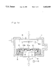
- FIG. 4 there is shown a reaction chamber 1 of a conventional dry etching apparatus which can be kept under a vacuum.
- a lower electrode 2 for holding a base material 4 is connected to a high frequency power source 7.
- a thin insulating layer 3 is provided on the upper surface of the lower electrode 2 as in contact with the entire rear surface of the to-be-processed base material 4.
- An upper electrode 6 is grounded and is provided with a reaction gas entrance (not shown).
- Reference numeral 5 designates an insulating spacer.
- the lower electrode 2 is made of aluminum and the insulating layer 3 is formed of hard aluminum obtained by anodizing aluminum, having a thickness of 20-80 ⁇ m.
- the lower electrode 2 is shown in detail in FIGS. 5A and 5B.
- reference numerals 8 and 9 designate a path along which cooling water flows to cool the base material 4 and a push-up mechanism to push the base material 4 upward so as to transfer the base material 4, respectively.
- the push-up mechanism 9 is moved up and down, the base material 4 is lowered onto the lower electrode 2 or is lifted up and then transferred.
- a reaction gas is introduced in the reaction chamber 1 and the reaction chamber is placed under a desired degree of vacuum.
- the high frequency power is supplied from the high frequency power source 7, plasma is generated and the base material 4 is etched.
- the base material 4 has a minus potential (approximately -500 V--1500 V) corresponding to the decreasing voltage of the cathode because of the plasma.
- the lower electrode 2 is covered with the insulating layer 3, a direct current potential is O V. Therefore, the base material 4 and the lower electrode 2 constitute the electrodes of a capacitor with the insulating layer 3 interposed therebetween, and the impression of the voltage to the capacitor brings about an electrostatic attraction force.
- the base material 4 is tightly adhered to the insulating layer 3 by the lower electrode 2. Accordingly, a good thermal conduction is achieved, and the temperature of the base material 4 becomes close to that of the lower electrode 2, thus making it possible to process the base material 4 at low temperatures.
- the temperature of the wafer after the electrostatic attraction is 40° C. Without the electrostatic attraction, that is, when the insulating layer 3 is not provided, the wafer is at 120° C.
- the minus charges stored in the base material 4 remain even after the power source 7 is turned OFF. Therefore, the electrostatic attraction continues, causing the base material 4 to leap and shift when the push-up mechanism 9 pushes the base material 4 upward as shown by dotted lines I and II in FIG. 5B.
- the base material 4 is not smoothly handed over to a transfer arm which, in the worst case, results in the base material 4 being broken.
- the output of the high frequency power source 7 can be lowered before the transfer of the base material 4 so as to decrease the charging potential of the base material 4 or N 2 gas can be blown in order to reduce the residual attraction force, it is hard to completely remove the residual attraction force.
- the object of the present invention is, therefore, to provide a dry etching apparatus capable of weakening the residual electrostatic attraction force so as to obviate transfer problems.
- an improved dry etching apparatus provided with flat parallel electrodes confronting each other, wherein a high frequency voltage is impressed between the electrodes, the improvement characterized in that the one electrode which supports a base material has a recess in its surface and the surface of the electrode is covered with an insulating layer, so that part of the structure constituted by the insulating layer and electrode is not in contact with the base material.
- FIG. 1A is a cross-sectional view of one embodiment of a dry etching apparatus of the present invention
- FIG. 1B is a plan view of an electrode of the apparatus shown in FIG. 1;
- FIG. 2 is a graph of the relationship of the opening ratio of recesses, the temperature of a base material and the residual electrostatic attraction force in the embodiment of the present invention
- FIG. 3 is a cross-sectional view of another embodiment of a dry etching apparatus of the present invention.
- FIG. 4 is a cross-sectional view of a conventional dry etching apparatus.
- FIGS. 5A and 5B are a plan view and a cross-sectional view of the detailed structure of a lower electrode in the conventional dry etching apparatus.
- FIG. 1A shows a reaction chamber 1 of one preferred embodiment of a dry etching apparatus of the present invention.
- the reaction chamber 1 can be maintained under a vacuum.
- a lower electrode 2 made of aluminum for holding a base material 4, such as a semiconducting substrate made of gallium arsenide, silicone, or glass, is connected to a high frequency power source 7.
- a high frequency power is supplied from the power source 7 to the lower electrode 2.
- a thin insulating layer 3 is formed at the upper surface of the lower electrode 2.
- An insulating spacer 5 upper electrode 6 confronting the lower electrode 2 is grounded and has a reaction gas entrance 6a.
- a reaction gas entrance is shown by a chain line in FIG. 1.
- the lower electrode 2 has in the upper surface thereof recesses 10 including a circular recess 10a at its center and an annular recess 10b extending around the circular recess 10a as shown in FIGS. 1A and 1B.
- the base material 4 is not close to the upper surface of the lower electrode 2.
- the 20-80 ⁇ m thick insulating layer 3 which is formed of hard anodized aluminum covers the entire upper surface of the lower electrode 2.
- the thickness of the hard aluminum is not less than 100 ⁇ and the thickness of the aluminum of the electrode is not less than 0.3 mm.
- material having a thermal conductivity that increases when in a vacuum is used for the insulating layer 3.
- the contact area between the insulating layer 3 and the base material is small.
- the relationship of the opening ratio of the recesses 10, the temperature of the base material 4 and the residual electrostatic attraction force is shown in a graph of FIG. 2. As is clear from FIG. 2, the residual attraction force is eliminated when the opening ratio is 20%. Although the temperature of the base material 4 is 10° C. higher when the opening ratio is 20% as compared to when there are not recesses, the increased temperature is not practically a problem. If the temperature of the cooling water for cooling the lower electrode 2 is lowered by approximately 10° C., the base material 4 can be at the same temperature as when the opening ratio is 0%.
- the lower electrode 2 has recesses 10 in the upper surface to thereby reduce the area of contact with the base material 4. Therefore, the residual attraction force is decreased, and the problems when the base material 4 is transferred can be solved.
- the opening ratio of the recesses and the cooling temperature of the electrode may be selected suitably.
- the opening ratio of the recesses 10 is not less than 20% with respect to a semiconducting substrate made of silicon. It is also preferred that the opening ratio of the recesses 10 not be less than 25% with respect to a semiconducting substrate made of glass.
- the lower electrode 2 has the recesses 10 in the upper surface thereof, and the insulating layer 3 is formed over the entire upper surface of the lower electrode 2.
- the insulating layer 3 may be formed while the upper surface of the lower electrode 2 is masked or the insulating layer 3 may be partially etched and removed after it is formed over the entire surface of the lower electrode 2.
- recesses 11 having a similar configuration to the recesses 10 are formed between the base material 4 and the lower electrode 2 where the insulating layer 3 is not present.
- the configuration of the recesses 10 and 11 may be changed as desired, e.g. the recesses may extend radially or be in the form of concentric circles.
- the electrode for holding a base material has a recess and the surface of the electrode is covered with the insulating layer so that part of the structure does not contact the base material.
- the surface of the electrode is covered with the insulating layer so that the insulating layer alone contacts the base material. Therefore, the area of contact with the base material is small, thus resulting in a weaker electrostatic attraction force. Since the residual electrostatic attraction force is reduced while the temperature rise of the base material on the electrode is restricted, the base material can be readily transferred.
Abstract
A dry etching apparatus is provided with parallel electrodes confronting each other, and a high frequency voltage is impressed between the electrodes. The electrode for holding a base material has a recess in its surface and the surface of the electrode is covered with an insulating layer so that part of the structure constituted by the insulating layer and electrode is not in contact with the base material.
Description
This application is a continuation of now abandoned application, Ser. No. 07/988,692, filed Dec. 10, 1992.
The present invention relates to a dry etching apparatus for use in the manufacture of semiconductors, thin film devices, etc.
Since such devices as referred to above have been increasingly miniaturized in recent years, severe requirements are demanded for a dry etching apparatus. For example, high dimensional accuracy, high anisotropic properties, high selectivity for a resist, an undercoating film or the like, etc. must be provided. In one device, the temperature of a wafer during etching has been controlled with good accuracy in an attempt to maintain the wafer at a low temperature.
An example of a conventional dry etching apparatus will be described below.
Referring to FIG. 4, there is shown a reaction chamber 1 of a conventional dry etching apparatus which can be kept under a vacuum. A lower electrode 2 for holding a base material 4 is connected to a high frequency power source 7. A thin insulating layer 3 is provided on the upper surface of the lower electrode 2 as in contact with the entire rear surface of the to-be-processed base material 4. An upper electrode 6 is grounded and is provided with a reaction gas entrance (not shown). Reference numeral 5 designates an insulating spacer.
Generally, the lower electrode 2 is made of aluminum and the insulating layer 3 is formed of hard aluminum obtained by anodizing aluminum, having a thickness of 20-80 μm.
The lower electrode 2 is shown in detail in FIGS. 5A and 5B. Referring to FIGS. 5A and 5B, reference numerals 8 and 9 designate a path along which cooling water flows to cool the base material 4 and a push-up mechanism to push the base material 4 upward so as to transfer the base material 4, respectively. When the push-up mechanism 9 is moved up and down, the base material 4 is lowered onto the lower electrode 2 or is lifted up and then transferred.
The operation of the dry etching apparatus having the above-described structure will now be described.
A reaction gas is introduced in the reaction chamber 1 and the reaction chamber is placed under a desired degree of vacuum. As the high frequency power is supplied from the high frequency power source 7, plasma is generated and the base material 4 is etched. At this time, the base material 4 has a minus potential (approximately -500 V--1500 V) corresponding to the decreasing voltage of the cathode because of the plasma. Since the lower electrode 2 is covered with the insulating layer 3, a direct current potential is O V. Therefore, the base material 4 and the lower electrode 2 constitute the electrodes of a capacitor with the insulating layer 3 interposed therebetween, and the impression of the voltage to the capacitor brings about an electrostatic attraction force. As a result of this, the base material 4 is tightly adhered to the insulating layer 3 by the lower electrode 2. Accordingly, a good thermal conduction is achieved, and the temperature of the base material 4 becomes close to that of the lower electrode 2, thus making it possible to process the base material 4 at low temperatures.
In one example, when a 6-inch wafer is processed for one minute with O2 gas, at 150 mTorr pressure, under 300 W of high frequency power at 13.56 MHz, and with a 100 mm distance between electrodes 2 and 6 while the lower electrode 2 is at 20° C., the temperature of the wafer after the electrostatic attraction is 40° C. Without the electrostatic attraction, that is, when the insulating layer 3 is not provided, the wafer is at 120° C.
In the above structure, the minus charges stored in the base material 4 remain even after the power source 7 is turned OFF. Therefore, the electrostatic attraction continues, causing the base material 4 to leap and shift when the push-up mechanism 9 pushes the base material 4 upward as shown by dotted lines I and II in FIG. 5B. The base material 4 is not smoothly handed over to a transfer arm which, in the worst case, results in the base material 4 being broken.
Although the output of the high frequency power source 7 can be lowered before the transfer of the base material 4 so as to decrease the charging potential of the base material 4 or N2 gas can be blown in order to reduce the residual attraction force, it is hard to completely remove the residual attraction force.
The object of the present invention is, therefore, to provide a dry etching apparatus capable of weakening the residual electrostatic attraction force so as to obviate transfer problems.
In accomplishing this and other objects according to the present invention, there is provided an improved dry etching apparatus provided with flat parallel electrodes confronting each other, wherein a high frequency voltage is impressed between the electrodes, the improvement characterized in that the one electrode which supports a base material has a recess in its surface and the surface of the electrode is covered with an insulating layer, so that part of the structure constituted by the insulating layer and electrode is not in contact with the base material.
This and other objects and features of the present invention will become clearer from the following description taken in conjunction with the preferred embodiments thereof with reference to the accompanying drawings throughout which like parts are designated by like reference numerals, and in which:
FIG. 1A is a cross-sectional view of one embodiment of a dry etching apparatus of the present invention;
FIG. 1B is a plan view of an electrode of the apparatus shown in FIG. 1;
FIG. 2 is a graph of the relationship of the opening ratio of recesses, the temperature of a base material and the residual electrostatic attraction force in the embodiment of the present invention;
FIG. 3 is a cross-sectional view of another embodiment of a dry etching apparatus of the present invention;
FIG. 4 is a cross-sectional view of a conventional dry etching apparatus; and
FIGS. 5A and 5B are a plan view and a cross-sectional view of the detailed structure of a lower electrode in the conventional dry etching apparatus.
A dry etching apparatus according to preferred embodiments of the present invention will be described hereinbelow with reference to FIGS. 1 and 2.
FIG. 1A shows a reaction chamber 1 of one preferred embodiment of a dry etching apparatus of the present invention. The reaction chamber 1 can be maintained under a vacuum. A lower electrode 2 made of aluminum for holding a base material 4, such as a semiconducting substrate made of gallium arsenide, silicone, or glass, is connected to a high frequency power source 7. A high frequency power is supplied from the power source 7 to the lower electrode 2. A thin insulating layer 3 is formed at the upper surface of the lower electrode 2. An insulating spacer 5 upper electrode 6 confronting the lower electrode 2 is grounded and has a reaction gas entrance 6a. Alternatively, a reaction gas entrance is shown by a chain line in FIG. 1.
The lower electrode 2 has in the upper surface thereof recesses 10 including a circular recess 10a at its center and an annular recess 10b extending around the circular recess 10a as shown in FIGS. 1A and 1B. At the recesses 10, the base material 4 is not close to the upper surface of the lower electrode 2. The 20-80 μm thick insulating layer 3 which is formed of hard anodized aluminum covers the entire upper surface of the lower electrode 2. Preferably, the thickness of the hard aluminum is not less than 100μ and the thickness of the aluminum of the electrode is not less than 0.3 mm. Preferably, material having a thermal conductivity that increases when in a vacuum is used for the insulating layer 3.
The operation of the dry etching apparatus having the above-described structure will be discussed below.
Since recesses 10 are formed in the surface of the lower electrode 2, the contact area between the insulating layer 3 and the base material is small. The relationship of the opening ratio of the recesses 10, the temperature of the base material 4 and the residual electrostatic attraction force is shown in a graph of FIG. 2. As is clear from FIG. 2, the residual attraction force is eliminated when the opening ratio is 20%. Although the temperature of the base material 4 is 10° C. higher when the opening ratio is 20% as compared to when there are not recesses, the increased temperature is not practically a problem. If the temperature of the cooling water for cooling the lower electrode 2 is lowered by approximately 10° C., the base material 4 can be at the same temperature as when the opening ratio is 0%.
In the embodiment described hereinabove, the lower electrode 2 has recesses 10 in the upper surface to thereby reduce the area of contact with the base material 4. Therefore, the residual attraction force is decreased, and the problems when the base material 4 is transferred can be solved.
Moreover, because the residual electrostatic attraction force may vary in dependence with kind of the base material 4, the opening ratio of the recesses and the cooling temperature of the electrode may be selected suitably. Preferably, the opening ratio of the recesses 10 is not less than 20% with respect to a semiconducting substrate made of silicon. It is also preferred that the opening ratio of the recesses 10 not be less than 25% with respect to a semiconducting substrate made of glass.
In the foregoing embodiment, the lower electrode 2 has the recesses 10 in the upper surface thereof, and the insulating layer 3 is formed over the entire upper surface of the lower electrode 2. However, it is possible to form the insulating layer 3 on only part of the upper surface of the lower electrode 2 without forming recesses in the electrode 2 itself as illustrated in FIG. 3. That is, the insulating layer 3 may be formed while the upper surface of the lower electrode 2 is masked or the insulating layer 3 may be partially etched and removed after it is formed over the entire surface of the lower electrode 2. In this case, recesses 11 having a similar configuration to the recesses 10 are formed between the base material 4 and the lower electrode 2 where the insulating layer 3 is not present.
The effect achieved in this case is the same as that in the first embodiment.
In the embodiments, the configuration of the recesses 10 and 11 may be changed as desired, e.g. the recesses may extend radially or be in the form of concentric circles.
According to one aspect of the present invention, the electrode for holding a base material has a recess and the surface of the electrode is covered with the insulating layer so that part of the structure does not contact the base material. Alternatively, only part of the surface of the electrode is covered with the insulating layer so that the insulating layer alone contacts the base material. Therefore, the area of contact with the base material is small, thus resulting in a weaker electrostatic attraction force. Since the residual electrostatic attraction force is reduced while the temperature rise of the base material on the electrode is restricted, the base material can be readily transferred.
Although the present invention has been fully described in connection with the preferred embodiments thereof with reference to the accompanying drawings, it is to be noted that various changes and modifications will become apparent to those skilled in the art. Such changes and modifications are to be understood as included within the scope of the present invention as defined by the appended claims unless they otherwise depart therefrom.
Claims (3)
1. In a dry etching process, the improvement comprising: providing an electrode having at least one recess in a surface thereof that faces toward another electrode disposed parallel thereto, and an insulating layer covering said surface; placing a base material atop said electrode with a rear surface of the base material contacting said insulating layer and covering said at least one recess in its entirety, said rear surface having such an area that the opening ratio of the entirety of the at least one recess over which the rear surface of the base material lies is not less than 20% with respect to said rear surface; and impressing a high frequency voltage between said electrodes.
2. A dry etching process comprising: providing an electrode having at least one recess in a surface thereof that faces toward another electrode disposed parallel thereto and wherein an insulating layer covers said surface; supporting a base material having a rear surface atop said electrode with the rear surface contacting said insulating layer and overlying said at least one recess in its entirety, the rear surface having such an area that the opening ratio of said at least one recess over which the rear surface of the base material lies is not more than 20% with respect to said rear surface; creating a vacuum in a space between said electrodes; and impressing a high frequency voltage between said electrodes.
3. The dry etching process as claimed in claim 2, and further comprising subsequently translating a push-up rod through said one of the electrodes to push the base material upward from the surface of said one of the electrodes.
Priority Applications (1)
| Application Number | Priority Date | Filing Date | Title |
|---|---|---|---|
| US08/202,882 US5443689A (en) | 1991-12-11 | 1994-02-28 | Dry etching process utilizing a recessed electrode |
Applications Claiming Priority (4)
| Application Number | Priority Date | Filing Date | Title |
|---|---|---|---|
| JP32718091A JP2758755B2 (en) | 1991-12-11 | 1991-12-11 | Dry etching apparatus and method |
| JP3-327180 | 1991-12-11 | ||
| US98869292A | 1992-12-10 | 1992-12-10 | |
| US08/202,882 US5443689A (en) | 1991-12-11 | 1994-02-28 | Dry etching process utilizing a recessed electrode |
Related Parent Applications (1)
| Application Number | Title | Priority Date | Filing Date |
|---|---|---|---|
| US98869292A Continuation | 1991-12-11 | 1992-12-10 |
Publications (1)
| Publication Number | Publication Date |
|---|---|
| US5443689A true US5443689A (en) | 1995-08-22 |
Family
ID=18196206
Family Applications (1)
| Application Number | Title | Priority Date | Filing Date |
|---|---|---|---|
| US08/202,882 Expired - Lifetime US5443689A (en) | 1991-12-11 | 1994-02-28 | Dry etching process utilizing a recessed electrode |
Country Status (3)
| Country | Link |
|---|---|
| US (1) | US5443689A (en) |
| JP (1) | JP2758755B2 (en) |
| KR (1) | KR950014076B1 (en) |
Cited By (14)
| Publication number | Priority date | Publication date | Assignee | Title |
|---|---|---|---|---|
| US5681419A (en) * | 1994-12-28 | 1997-10-28 | Hyundai Electronics Industries Co., Ltd. | Reactive ion etching apparatus |
| US5792304A (en) * | 1993-09-16 | 1998-08-11 | Hitachi, Ltd. | Method of holding substrate and substrate holding system |
| US5958140A (en) * | 1995-07-27 | 1999-09-28 | Tokyo Electron Limited | One-by-one type heat-processing apparatus |
| US5976309A (en) * | 1996-12-17 | 1999-11-02 | Lsi Logic Corporation | Electrode assembly for plasma reactor |
| US6228438B1 (en) * | 1999-08-10 | 2001-05-08 | Unakis Balzers Aktiengesellschaft | Plasma reactor for the treatment of large size substrates |
| US20020173161A1 (en) * | 2001-04-05 | 2002-11-21 | Matsushita Electric Industrial Co., Ltd. | Plasma processing method |
| US6524428B2 (en) | 1993-09-16 | 2003-02-25 | Hitachi, Ltd. | Method of holding substrate and substrate holding system |
| WO2003075333A1 (en) * | 2002-03-04 | 2003-09-12 | Ci Science, Inc. | Electrode for dry etching a wafer |
| US6712019B2 (en) * | 1996-02-08 | 2004-03-30 | Canon Kabushiki Kaisha | Film forming apparatus having electrically insulated element that introduces power of 20-450MHz |
| US20040173469A1 (en) * | 2003-03-04 | 2004-09-09 | Ryujiro Udo | Plasma processing apparatus and method for manufacturing electrostatic chuck |
| US20050023254A1 (en) * | 2002-02-28 | 2005-02-03 | Daisuke Hayashi | Plasma processing apparatus, electrode unit, feeder member and radio frequency feeder rod |
| WO2006088114A1 (en) * | 2005-02-15 | 2006-08-24 | Matsushita Electric Industrial Co., Ltd. | Plasma treatment apparatus |
| WO2007032418A1 (en) * | 2005-09-12 | 2007-03-22 | Matsushita Electric Industrial Co., Ltd. | Plasma treating apparatus and electrode member therefor and electrode member manufacturing and recycling method |
| US20150044424A1 (en) * | 2013-02-19 | 2015-02-12 | Boe Technology Group Co., Ltd. | Bottom electrode and manufacturing method thereof |
Families Citing this family (3)
| Publication number | Priority date | Publication date | Assignee | Title |
|---|---|---|---|---|
| US7232591B2 (en) | 2002-04-09 | 2007-06-19 | Matsushita Electric Industrial Co., Ltd. | Method of using an adhesive for temperature control during plasma processing |
| KR100511854B1 (en) | 2002-06-18 | 2005-09-02 | 아네르바 가부시키가이샤 | Electrostatic chuck device |
| CN100345274C (en) * | 2003-02-27 | 2007-10-24 | 株式会社日立高新技术 | Method of producing electrostatic suction cup |
Citations (7)
| Publication number | Priority date | Publication date | Assignee | Title |
|---|---|---|---|---|
| JPS5555530A (en) * | 1978-10-18 | 1980-04-23 | Takuo Sugano | Electrode device for plasma processor |
| JPS59181620A (en) * | 1983-03-31 | 1984-10-16 | Toshiba Corp | Reactive-ion etching method |
| US4793975A (en) * | 1985-05-20 | 1988-12-27 | Tegal Corporation | Plasma Reactor with removable insert |
| US4897171A (en) * | 1985-11-26 | 1990-01-30 | Tadahiro Ohmi | Wafer susceptor |
| JPH02155230A (en) * | 1988-12-07 | 1990-06-14 | Matsushita Electric Ind Co Ltd | Dry etching system |
| US4968374A (en) * | 1988-06-09 | 1990-11-06 | Anelva Corporation | Plasma etching apparatus with dielectrically isolated electrodes |
| JPH0429315A (en) * | 1990-05-24 | 1992-01-31 | Matsushita Electric Ind Co Ltd | Plasma treatment device |
Family Cites Families (1)
| Publication number | Priority date | Publication date | Assignee | Title |
|---|---|---|---|---|
| JPH0722150B2 (en) * | 1984-03-07 | 1995-03-08 | 株式会社日立製作所 | Plasma processing device |
-
1991
- 1991-12-11 JP JP32718091A patent/JP2758755B2/en not_active Expired - Fee Related
-
1992
- 1992-12-09 KR KR1019920023687A patent/KR950014076B1/en not_active IP Right Cessation
-
1994
- 1994-02-28 US US08/202,882 patent/US5443689A/en not_active Expired - Lifetime
Patent Citations (7)
| Publication number | Priority date | Publication date | Assignee | Title |
|---|---|---|---|---|
| JPS5555530A (en) * | 1978-10-18 | 1980-04-23 | Takuo Sugano | Electrode device for plasma processor |
| JPS59181620A (en) * | 1983-03-31 | 1984-10-16 | Toshiba Corp | Reactive-ion etching method |
| US4793975A (en) * | 1985-05-20 | 1988-12-27 | Tegal Corporation | Plasma Reactor with removable insert |
| US4897171A (en) * | 1985-11-26 | 1990-01-30 | Tadahiro Ohmi | Wafer susceptor |
| US4968374A (en) * | 1988-06-09 | 1990-11-06 | Anelva Corporation | Plasma etching apparatus with dielectrically isolated electrodes |
| JPH02155230A (en) * | 1988-12-07 | 1990-06-14 | Matsushita Electric Ind Co Ltd | Dry etching system |
| JPH0429315A (en) * | 1990-05-24 | 1992-01-31 | Matsushita Electric Ind Co Ltd | Plasma treatment device |
Non-Patent Citations (2)
| Title |
|---|
| Alfred Johnsen et al., "A Physical Phenomenon and its Applications to Telegraphy, Telephony, etc.", IEE Journal, vol. 61, No. 320, pp. 713-715 Jul. 1923. |
| Alfred Johnsen et al., A Physical Phenomenon and its Applications to Telegraphy, Telephony, etc. , IEE Journal, vol. 61, No. 320, pp. 713 715 Jul. 1923. * |
Cited By (36)
| Publication number | Priority date | Publication date | Assignee | Title |
|---|---|---|---|---|
| US6676805B2 (en) | 1993-09-16 | 2004-01-13 | Hitachi, Ltd. | Method of holding substrate and substrate holding system |
| US6899789B2 (en) | 1993-09-16 | 2005-05-31 | Hitachi, Ltd. | Method of holding substrate and substrate holding system |
| US20030192647A1 (en) * | 1993-09-16 | 2003-10-16 | Naoyuki Tamura | Method of holding substrate and substrate holding system |
| US6645871B2 (en) | 1993-09-16 | 2003-11-11 | Hitachi, Ltd. | Method of holding substrate and substrate holding system |
| US5961774A (en) * | 1993-09-16 | 1999-10-05 | Hitachi, Ltd. | Method of holding substrate and substrate holding system |
| US5792304A (en) * | 1993-09-16 | 1998-08-11 | Hitachi, Ltd. | Method of holding substrate and substrate holding system |
| US5985035A (en) * | 1993-09-16 | 1999-11-16 | Hitachi, Ltd. | Method of holding substrate and substrate holding system |
| US6221201B1 (en) | 1993-09-16 | 2001-04-24 | Hitachi, Ltd. | Method of holding substrate and substrate holding system |
| US5906684A (en) * | 1993-09-16 | 1999-05-25 | Hitachi, Ltd. | Method of holding substrate and substrate holding system |
| US6336991B1 (en) * | 1993-09-16 | 2002-01-08 | Hitachi, Ltd. | Method of holding substrate and substrate holding system |
| US6610171B2 (en) | 1993-09-16 | 2003-08-26 | Hitachi, Ltd. | Method of holding substrate and substrate holding system |
| US6524428B2 (en) | 1993-09-16 | 2003-02-25 | Hitachi, Ltd. | Method of holding substrate and substrate holding system |
| US6544379B2 (en) * | 1993-09-16 | 2003-04-08 | Hitachi, Ltd. | Method of holding substrate and substrate holding system |
| US6610170B2 (en) | 1993-09-16 | 2003-08-26 | Hitachi, Ltd. | Method of holding substrate and substrate holding system |
| US5681419A (en) * | 1994-12-28 | 1997-10-28 | Hyundai Electronics Industries Co., Ltd. | Reactive ion etching apparatus |
| US5958140A (en) * | 1995-07-27 | 1999-09-28 | Tokyo Electron Limited | One-by-one type heat-processing apparatus |
| US6712019B2 (en) * | 1996-02-08 | 2004-03-30 | Canon Kabushiki Kaisha | Film forming apparatus having electrically insulated element that introduces power of 20-450MHz |
| US6767593B2 (en) | 1996-02-08 | 2004-07-27 | Canon Kabushiki Kaisha | Apparatus and process for forming a deposited film |
| US20040079288A1 (en) * | 1996-02-08 | 2004-04-29 | Kazuyoshi Akiyama | Apparatus and process for forming a deposited film |
| US5976309A (en) * | 1996-12-17 | 1999-11-02 | Lsi Logic Corporation | Electrode assembly for plasma reactor |
| US6228438B1 (en) * | 1999-08-10 | 2001-05-08 | Unakis Balzers Aktiengesellschaft | Plasma reactor for the treatment of large size substrates |
| US20020173161A1 (en) * | 2001-04-05 | 2002-11-21 | Matsushita Electric Industrial Co., Ltd. | Plasma processing method |
| US6867146B2 (en) * | 2001-04-05 | 2005-03-15 | Matsushita Electric Industrial Co., Ltd. | Plasma processing method |
| US20050023254A1 (en) * | 2002-02-28 | 2005-02-03 | Daisuke Hayashi | Plasma processing apparatus, electrode unit, feeder member and radio frequency feeder rod |
| US20070284085A1 (en) * | 2002-02-28 | 2007-12-13 | Daisuke Hayashi | Plasma processing apparatus, electrode unit, feeder member and radio frequency feeder rod |
| US7230202B2 (en) * | 2002-02-28 | 2007-06-12 | Tokyo Electron Limited | Plasma processing apparatus, electrode unit, feeder member and radio frequency feeder rod |
| WO2003075333A1 (en) * | 2002-03-04 | 2003-09-12 | Ci Science, Inc. | Electrode for dry etching a wafer |
| US20050178505A1 (en) * | 2002-03-04 | 2005-08-18 | Young Yul Kim | Electrode for dry etching a wafer |
| US20060121195A1 (en) * | 2003-02-24 | 2006-06-08 | Ryujiro Udo | Plasma processing apparatus and method for manufacturing electrostatic chuck |
| US20040173469A1 (en) * | 2003-03-04 | 2004-09-09 | Ryujiro Udo | Plasma processing apparatus and method for manufacturing electrostatic chuck |
| WO2006088114A1 (en) * | 2005-02-15 | 2006-08-24 | Matsushita Electric Industrial Co., Ltd. | Plasma treatment apparatus |
| US8016974B2 (en) | 2005-02-15 | 2011-09-13 | Panasonic Corporation | Plasma treatment apparatus |
| US20080251208A1 (en) * | 2005-02-15 | 2008-10-16 | Tetsuo Korenaga | Plasma Treatment Apparatus |
| WO2007032418A1 (en) * | 2005-09-12 | 2007-03-22 | Matsushita Electric Industrial Co., Ltd. | Plasma treating apparatus and electrode member therefor and electrode member manufacturing and recycling method |
| US20090011120A1 (en) * | 2005-09-12 | 2009-01-08 | Matsushita Electric Industrial Co., Ltd | Plasma Treating Apparatus, Electrode Member for Plasma Treating Apparatus, Electrode Member Manufacturing Method and Recycling Method |
| US20150044424A1 (en) * | 2013-02-19 | 2015-02-12 | Boe Technology Group Co., Ltd. | Bottom electrode and manufacturing method thereof |
Also Published As
| Publication number | Publication date |
|---|---|
| KR930013208A (en) | 1993-07-21 |
| KR950014076B1 (en) | 1995-11-21 |
| JP2758755B2 (en) | 1998-05-28 |
| JPH05160076A (en) | 1993-06-25 |
Similar Documents
| Publication | Publication Date | Title |
|---|---|---|
| US5443689A (en) | Dry etching process utilizing a recessed electrode | |
| US7160392B2 (en) | Method for dechucking a substrate | |
| JP3082624B2 (en) | How to use electrostatic chuck | |
| US5847918A (en) | Electrostatic clamping method and apparatus for dielectric workpieces in vacuum processors | |
| US7667945B2 (en) | Bipolar carrier wafer and mobile bipolar electrostatic wafer arrangement | |
| US20040072426A1 (en) | Process chamber for manufacturing a smiconductor device | |
| JP2000502837A (en) | Electrostatic clamp with lip seal for board clamp | |
| KR20210119296A (en) | Edge ring, substrate support, plasma processing system and method of replacing edge ring | |
| JPH0622213B2 (en) | Sample temperature control method and apparatus | |
| JP3113796B2 (en) | Plasma processing equipment | |
| JPH07335570A (en) | Control method of substrate temperature in plasma treatment | |
| US11398397B2 (en) | Electrostatic chuck and plasma processing apparatus including the same | |
| JP2580791B2 (en) | Vacuum processing equipment | |
| JPH07183280A (en) | Plasma treatment device | |
| JPH0670984B2 (en) | Sample temperature control method and apparatus | |
| JPS63131519A (en) | Dry etching apparatus | |
| JPH07312362A (en) | Dry etching device | |
| JP3587919B2 (en) | Method for manufacturing semiconductor device | |
| JPH07273176A (en) | Sample holding method for vacuum processing system | |
| JP2636781B2 (en) | Vacuum processing method | |
| JPH02110927A (en) | Specimen holding device | |
| KR20030000768A (en) | electro static chuck with shadow ring | |
| JP2636782B2 (en) | Control method of heat transfer gas for sample temperature control | |
| KR20030008724A (en) | Electrostatic Chuck with Improved Chucking capability in Edge thereof | |
| KR20050102378A (en) | Electrostatic chuck structure in semiconductor fabrication equipment |
Legal Events
| Date | Code | Title | Description |
|---|---|---|---|
| STCF | Information on status: patent grant |
Free format text: PATENTED CASE |
|
| FEPP | Fee payment procedure |
Free format text: PAYOR NUMBER ASSIGNED (ORIGINAL EVENT CODE: ASPN); ENTITY STATUS OF PATENT OWNER: LARGE ENTITY |
|
| FPAY | Fee payment |
Year of fee payment: 4 |
|
| FPAY | Fee payment |
Year of fee payment: 8 |
|
| FPAY | Fee payment |
Year of fee payment: 12 |