US5447067A - Acceleration sensor and method for manufacturing same - Google Patents
Acceleration sensor and method for manufacturing same Download PDFInfo
- Publication number
- US5447067A US5447067A US08/207,080 US20708094A US5447067A US 5447067 A US5447067 A US 5447067A US 20708094 A US20708094 A US 20708094A US 5447067 A US5447067 A US 5447067A
- Authority
- US
- United States
- Prior art keywords
- proof mass
- silicon layer
- electrodes
- substrate
- resilient element
- Prior art date
- Legal status (The legal status is an assumption and is not a legal conclusion. Google has not performed a legal analysis and makes no representation as to the accuracy of the status listed.)
- Expired - Lifetime
Links
Images

Classifications
-
- G—PHYSICS
- G01—MEASURING; TESTING
- G01P—MEASURING LINEAR OR ANGULAR SPEED, ACCELERATION, DECELERATION, OR SHOCK; INDICATING PRESENCE, ABSENCE, OR DIRECTION, OF MOVEMENT
- G01P15/00—Measuring acceleration; Measuring deceleration; Measuring shock, i.e. sudden change of acceleration
- G01P15/02—Measuring acceleration; Measuring deceleration; Measuring shock, i.e. sudden change of acceleration by making use of inertia forces using solid seismic masses
- G01P15/08—Measuring acceleration; Measuring deceleration; Measuring shock, i.e. sudden change of acceleration by making use of inertia forces using solid seismic masses with conversion into electric or magnetic values
- G01P15/125—Measuring acceleration; Measuring deceleration; Measuring shock, i.e. sudden change of acceleration by making use of inertia forces using solid seismic masses with conversion into electric or magnetic values by capacitive pick-up
-
- G—PHYSICS
- G01—MEASURING; TESTING
- G01P—MEASURING LINEAR OR ANGULAR SPEED, ACCELERATION, DECELERATION, OR SHOCK; INDICATING PRESENCE, ABSENCE, OR DIRECTION, OF MOVEMENT
- G01P15/00—Measuring acceleration; Measuring deceleration; Measuring shock, i.e. sudden change of acceleration
- G01P15/02—Measuring acceleration; Measuring deceleration; Measuring shock, i.e. sudden change of acceleration by making use of inertia forces using solid seismic masses
- G01P15/08—Measuring acceleration; Measuring deceleration; Measuring shock, i.e. sudden change of acceleration by making use of inertia forces using solid seismic masses with conversion into electric or magnetic values
- G01P15/0802—Details
-
- G—PHYSICS
- G01—MEASURING; TESTING
- G01P—MEASURING LINEAR OR ANGULAR SPEED, ACCELERATION, DECELERATION, OR SHOCK; INDICATING PRESENCE, ABSENCE, OR DIRECTION, OF MOVEMENT
- G01P15/00—Measuring acceleration; Measuring deceleration; Measuring shock, i.e. sudden change of acceleration
- G01P15/02—Measuring acceleration; Measuring deceleration; Measuring shock, i.e. sudden change of acceleration by making use of inertia forces using solid seismic masses
- G01P15/08—Measuring acceleration; Measuring deceleration; Measuring shock, i.e. sudden change of acceleration by making use of inertia forces using solid seismic masses with conversion into electric or magnetic values
- G01P15/12—Measuring acceleration; Measuring deceleration; Measuring shock, i.e. sudden change of acceleration by making use of inertia forces using solid seismic masses with conversion into electric or magnetic values by alteration of electrical resistance
- G01P15/123—Measuring acceleration; Measuring deceleration; Measuring shock, i.e. sudden change of acceleration by making use of inertia forces using solid seismic masses with conversion into electric or magnetic values by alteration of electrical resistance by piezo-resistive elements, e.g. semiconductor strain gauges
-
- G—PHYSICS
- G01—MEASURING; TESTING
- G01P—MEASURING LINEAR OR ANGULAR SPEED, ACCELERATION, DECELERATION, OR SHOCK; INDICATING PRESENCE, ABSENCE, OR DIRECTION, OF MOVEMENT
- G01P15/00—Measuring acceleration; Measuring deceleration; Measuring shock, i.e. sudden change of acceleration
- G01P15/02—Measuring acceleration; Measuring deceleration; Measuring shock, i.e. sudden change of acceleration by making use of inertia forces using solid seismic masses
- G01P15/08—Measuring acceleration; Measuring deceleration; Measuring shock, i.e. sudden change of acceleration by making use of inertia forces using solid seismic masses with conversion into electric or magnetic values
- G01P2015/0805—Measuring acceleration; Measuring deceleration; Measuring shock, i.e. sudden change of acceleration by making use of inertia forces using solid seismic masses with conversion into electric or magnetic values being provided with a particular type of spring-mass-system for defining the displacement of a seismic mass due to an external acceleration
- G01P2015/0808—Measuring acceleration; Measuring deceleration; Measuring shock, i.e. sudden change of acceleration by making use of inertia forces using solid seismic masses with conversion into electric or magnetic values being provided with a particular type of spring-mass-system for defining the displacement of a seismic mass due to an external acceleration for defining in-plane movement of the mass, i.e. movement of the mass in the plane of the substrate
- G01P2015/0811—Measuring acceleration; Measuring deceleration; Measuring shock, i.e. sudden change of acceleration by making use of inertia forces using solid seismic masses with conversion into electric or magnetic values being provided with a particular type of spring-mass-system for defining the displacement of a seismic mass due to an external acceleration for defining in-plane movement of the mass, i.e. movement of the mass in the plane of the substrate for one single degree of freedom of movement of the mass
- G01P2015/0814—Measuring acceleration; Measuring deceleration; Measuring shock, i.e. sudden change of acceleration by making use of inertia forces using solid seismic masses with conversion into electric or magnetic values being provided with a particular type of spring-mass-system for defining the displacement of a seismic mass due to an external acceleration for defining in-plane movement of the mass, i.e. movement of the mass in the plane of the substrate for one single degree of freedom of movement of the mass for translational movement of the mass, e.g. shuttle type
Definitions
- the present invention is directed to an acceleration sensor, and in particular to an acceleration sensor constructed on an SOI (silicon-on-insulator) substrate, for exact measurement of minute accelerations, as well as to a method for manufacturing such an acceleration sensor.
- SOI silicon-on-insulator
- the mechanical long-term stability of these parts is inadequate under certain circumstances in comparison to the expected service life of the systems in which they are utilized.
- the mechanical properties of such parts such as the modulus of elasticity and the intrinsic stress of the layers, are sensitively dependent on the particular manufacturing conditions.
- the thermal curing of the intrinsic stress of the layers requires additional temperature steps in the manufacturing process, which have a disadvantageous effect on the simultaneously manufactured electronics which are integrated in the sensor.
- long-lasting and complicated depositions of semiconductor layers are necessary.
- an acceleration sensor having a proof mass attached to one or more resilient spring elements, the proof mass and the resilient elements being formed in a monocrystalline silicon layer of a SOI substrate, with the insulator layer of the substrate being removed in a region which is sufficiently large to permit free mobility of the proof mass.
- Means are provided for determining the excursion (amount of displacement) of the proof mass due to acceleration from a quiescent position.
- the acceleration sensor of the invention avoids the disadvantages associated with the use of polysilicon layers for the mechanically movable parts, by instead using single-crystal silicon for these parts.
- Monocrystalline silicon has precisely known mechanical properties, which are not dependent on the particular parameters of the manufacturing process used to make the parts. Moreover, the mechanical properties are not subject to chronological degradation, so that the long-term stability is better.
- the use of SOI substrates is particularly advantageous, because in such substrates, the monocrystalline silicon layer is located on the insulator layer.
- the main constituent of these substrates can be a monocrystalline silicon body, so that two monocrystalline silicon layers are separated by an intervening insulator layer.
- the mechanically moving parts are fashioned in the silicon layer, on the insulator layer, and the insulator layer is removed beneath the structured region of the silicon layer in order to enable the free mobility of the micromechanical parts.
- FIG. 1 is a plan view of a first embodiment of an acceleration sensor constructed in accordance with the principles of the present invention, in the form of a piezoresistive acceleration sensor.
- FIG. 2 is a plan view of a second embodiment of an acceleration sensor constructed in accordance with the principles of the present invention in the form of a capacitive acceleration sensor.
- FIG. 3 is a plan view of a third embodiment of an acceleration sensor constructed in accordance with the principles of the present invention, also in the form of a capacitive acceleration sensor.
- FIG. 4 is a plan view of a fourth embodiment of an acceleration sensor constructed in accordance with the principles of the present invention, also in the form of a capacitive acceleration sensor.
- FIG. 1 shows the structure of a piezoresistive acceleration sensor on an SOI substrate in a plan view.
- the structure of the mechanical parts is etched out of the upper, monocrystalline silicon layer 1 of the substrate.
- a proof mass 2 is suspended by one or more resilient elements 3, and is connected via the resilient elements 3 to the remaining portion of the silicon layer 1.
- Piezoresistors 4, which change their electrical resistance dependent on a mechanical deformation thereof, are disposed at the location at which the resilient elements 3 are secured to the silicon layer 1.
- the silicon layer 1 is sufficiently doped so as to be electrically conductive, so that a change in the resistance of the piezoresistors 4 can be identified.
- the piezoresistors 4 can be attached at arbitrary locations of the resilient elements 3, as long as they are disposed at a location which is subject to mechanical deformation as a result of the acceleration to which the sensor is subjected.
- the piezoresistors 4 are attached at locations at which the material of the silicon layer 1 is particularly highly deformed given a movement of the proof mass 2.
- the insulator layer is removed beneath the proof mass 2 and beneath the resilient elements 3 in a region sufficiently large to permit mobility of the proof mass 2.
- the proof mass 2 can be provided with holes in order to facilitate the removal of this insulator layer during manufacture. If the width of the resilient elements 3, i.e., their lateral dimension in the plan view shown in FIG. 1, is small in comparison to their thickness, the axis of the principal sensitivity of the sensor will lie in the plane of the silicon layer 1.
- the axis of the principal sensitivity of the sensor will be perpendicular to the silicon layer 1.
- the direction of an acceleration to be detected is perpendicular to the longitudinal direction of the resilient elements 3.
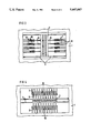
- FIG. 2 shows the structure of an acceleration sensor in plan view wherein a capacitive measurement of the acceleration is undertaken.
- the micromechanical elements are again etched out of the upper, single-crystal silicon layer 1 of the substrate.
- the proof mass 2 is connected to the remaining portion of the silicon layer 1 by means of resilient elements 3.
- the proof mass 2 is doped so as to be electrically conductive, and forms a capacitor in combination with corresponding, doped regions in the silicon layer 1, which are disposed opposite the proof mass 2, and form the cooperating electrodes 5.
- the proof mass 2 thus forms a separate capacitor with each of the electrodes 5.
- capacitors are arranged so that the respective capacitances thereof change as a consequence of the modified spacing of the conductors which occurs given a movement of the proof mass 2 perpendicular to the longitudinal direction of the resilient elements 3.
- This change in the capacitances ensues oppositely at the respective capacitors disposed at the opposite sides of the proof mass 2.
- the acceleration can therefore be directly identified from the difference between the respective capacitance changes of the two capacitors.
- the force acting perpendicularly relative to the longitudinal direction of the resilient elements 3 due to an acceleration in the plane of the silicon layer 1 can be compensated by applying an appropriate polarization voltage to the doped electrodes of the capacitors.
- the measured signal is highly linearized, and the range of measurement is expanded, the resilient constant of the suspension of the proof mass 2 formed by the resilient elements 3 being negligible in a first approximation.
- This structure is suitable for detecting accelerations in the plane of the silicon layer 1 perpendicular to the longitudinal direction of the resilient elements 3.
- FIG. 3 shows a further version of a capacitively measuring acceleration sensor in plan view wherein the capacitors are formed by finger-shaped electrodes.
- the proof mass 2 is connected to the remaining portion of the silicon layer 1 by resilient elements 3.
- the proof mass 2 is shown in FIG. 3 with holes therein, which make the insulator layer beneath the proof mass 2 more easily accessible for being etched away during manufacture.
- Finger-shaped electrodes 6, which are doped so as to be electrically conductive, are located at the proof mass 2.
- the electrodes 6 form a plurality of capacitors together with corresponding, finger-shaped electrodes 7 and 8, respectively disposed on opposite sides of each electrode 6 and connected to the remaining silicon layer 1.
- An acceleration of the proof mass 2 in the plane of the silicon layer 1, perpendicular to the resilient elements 3, causes a change in capacitance between one of the finger-shaped electrodes 6 of the proof mass 2 and one of the electrodes 7 and 8 of the silicon layer 1 arranged next to the electrode 6.
- the electrodes 7 on each side of the proof mass 2 are all electrically connected together, so as to form a group of capacitors 91 in combination with the electrodes 6.
- the measured signal is extremely highly linearized, and the range of measurement is expanded, and a possible change in the spring constant of the spring elements 3, given larger excursions, need not be taken into consideration in the calculation which takes place in an evaluation circuit (not shown) connected to each of the capacitors.
- This structure is suitable for detecting accelerations in the plane of the silicon layer 1 perpendicular to the longitudinal direction of the resilient elements 3.
- FIG. 4 shows a further version of an acceleration sensor wherein a capacitative measurement of acceleration is undertaken, wherein the excursion of the proof mass 2 ensues in the longitudinal direction of the finger-shaped electrodes.
- An acceleration of the substrate perpendicular to the longitudinal direction of the resilient elements 3, holding the proof mass 2 is also detected in the embodiment of FIG. 4.
- the finger-shaped electrodes 6 applied to the proof mass 2 are arranged so that their longitudinal directions extend perpendicularly to the longitudinal direction of the resilient elements 3.
- Interdigital capacitors 91 and 92 are thus formed at each side of the proof mass 2. These two capacitors 91 and 92 respectively change their capacitance in opposite directions given an acceleration of the substrate, and thus an excursion of the proof mass 2 in the plane of the silicon layer 1 perpendicular to the longitudinal direction of the resilient elements 3. The acceleration can be directly identified from the difference between the capacitance changes of the two capacitors 91 and 92.
- Each of the above embodiments regardless of the individual structure thereof, includes a proof mass which is suspended by one or more resilient elements, with the proof mass and the springs being fashioned in the silicon layer of an SOI substrate.
- the ratio of the width-to-thickness of the spring elements defines the direction of the sensitivity of the acceleration sensor (perpendicular to the longitudinal direction of the spring elements).
- a measurement of the inertial force acting on the proof mass 2 as a consequence of an acceleration of the substrate can be undertaken substantially more precisely in the embodiments wherein the measurement is made capacitively, as opposed to the embodiment employing a piezoresistor.
- Such a capacitively measuring acceleration sensor is less dependent on temperature.
- capacitively measuring sensors can be more easily manufactured in large quantity given low tolerances.
- a capacitive measurement also has the advantage that the inertial forces which arise can be compensated by electrostatic forces, by applying appropriate potentials to the electrodes of the capacitors. It is theoretically possible also to measure accelerations capacitively arising perpendicularly to the plane of the silicon layer, with an appropriate embodiment of the acceleration sensor of the invention. In such an embodiment, however, a cooperating electrode above the plane of the proof mass 2 would then be required, in addition to a substrate electrode, so that the differences in the capacitance changes occurring above and below the proof mass 2 could be measured.
- This cooperating electrode which simplifies the measurement, may be formed, for example, by a further layer produced by applying a polysilicon layer onto the SOI substrate.
- the sensor of the invention is manufactured by electrically doping an SOI substrate so as to render the substrate conductive, at least in the regions required for the electrical conductors for the piezoresistors, or for the capacitors and their terminals.
- the silicon layer is then structured, for example, using a lithographic process (for example, electron beam lithography).
- the micromechanical parts are formed in the silicon layer by removing portions of the silicon layer in an etching process (for example, anisotropic dry etching).
- the material of the insulator layer (for example, SiO 2 ) situated beneath the manufactured structure is removed with a further etching process (for example, wet chemical etching).
- sublimating chemicals for example, cyclohexane or dichlorobenzene
- the electronic circuit is first produced up to the metallization stage.
- the parts of the substrate which do not belong to the sensor are covered with a protective layer, for example, photoresist, and the micromechanical elements are then produced and the protective layer is subsequently removed.
- the deposition of an additional layer is eliminated in the manufacturing process, thereby simplifying the manufacturing process. Moreover, no tempering for curing the intrinsic stress of the mechanical components is required. Electronic components integrated in the substrate are therefore not influenced at all, in terms of their electrical properties, by the manufacture of the sensor part. The most modern manufacturing processes for generating small structural sizes can therefore be utilized for the electronic elements. Sensors with integrated electronics can therefore be manufactured with extremely small dimensions. The overall manufacturing process is thereby further simplified. An arrangement of a plurality of sensors as disclosed herein in a sensor array, for detecting acceleration in three orthogonal spatial directions, is possible in a simple manner. High precision, even for detecting minutes accelerations, with high long-term stability, are ensured.
Abstract
Description
Claims (7)
Applications Claiming Priority (2)
| Application Number | Priority Date | Filing Date | Title |
|---|---|---|---|
| DE4310352 | 1993-03-30 | ||
| DE4310352.9 | 1993-03-30 |
Publications (1)
| Publication Number | Publication Date |
|---|---|
| US5447067A true US5447067A (en) | 1995-09-05 |
Family
ID=6484251
Family Applications (1)
| Application Number | Title | Priority Date | Filing Date |
|---|---|---|---|
| US08/207,080 Expired - Lifetime US5447067A (en) | 1993-03-30 | 1994-03-08 | Acceleration sensor and method for manufacturing same |
Country Status (5)
| Country | Link |
|---|---|
| US (1) | US5447067A (en) |
| EP (1) | EP0618450A1 (en) |
| JP (1) | JPH06302832A (en) |
| KR (1) | KR940022091A (en) |
| TW (1) | TW230237B (en) |
Cited By (51)
| Publication number | Priority date | Publication date | Assignee | Title |
|---|---|---|---|---|
| US5569852A (en) * | 1994-01-05 | 1996-10-29 | Robert Bosch Gmbh | Capacitive accelerometer sensor and method for its manufacture |
| US5578755A (en) * | 1993-12-03 | 1996-11-26 | Robert Bosch Gmbh | Accelerometer sensor of crystalline material and method for manufacturing the same |
| US5604312A (en) * | 1994-11-25 | 1997-02-18 | Robert Bosch Gmbh | Rate-of-rotation sensor |
| EP0810441A2 (en) * | 1996-05-30 | 1997-12-03 | Texas Instruments Incorporated | Composite sensor |
| WO1998011443A1 (en) * | 1996-09-13 | 1998-03-19 | Robert Bosch Gmbh | Sensor for capacitively recording an acceleration |
| US5731229A (en) * | 1994-06-28 | 1998-03-24 | Nissan Motor Co., Ltd. | Method of producing device having minute structure |
| US5734105A (en) * | 1992-10-13 | 1998-03-31 | Nippondenso Co., Ltd. | Dynamic quantity sensor |
| US5747353A (en) * | 1996-04-16 | 1998-05-05 | National Semiconductor Corporation | Method of making surface micro-machined accelerometer using silicon-on-insulator technology |
| US5750904A (en) * | 1994-08-16 | 1998-05-12 | Siemens Aktiengesellschaft | Force a displacement sensor with a capacitive transducer |
| US5818093A (en) * | 1996-01-25 | 1998-10-06 | Motorola, Inc. | Semiconductor device having a movable gate |
| US5851851A (en) * | 1994-03-07 | 1998-12-22 | Nippondenso Co., Ltd. | Method for fabricating a semiconductor acceleration sensor |
| US5880369A (en) * | 1996-03-15 | 1999-03-09 | Analog Devices, Inc. | Micromachined device with enhanced dimensional control |
| US5905203A (en) * | 1995-11-07 | 1999-05-18 | Temic Telefunken Microelectronic Gmbh | Micromechanical acceleration sensor |
| US5911157A (en) * | 1994-01-18 | 1999-06-08 | Siemens Aktiengesellschaft | Tunnel effect sensor |
| US5959208A (en) * | 1995-02-08 | 1999-09-28 | Robert Bosch GmbH | Acceleration sensor |
| US5992233A (en) * | 1996-05-31 | 1999-11-30 | The Regents Of The University Of California | Micromachined Z-axis vibratory rate gyroscope |
| US6000280A (en) * | 1995-07-20 | 1999-12-14 | Cornell Research Foundation, Inc. | Drive electrodes for microfabricated torsional cantilevers |
| US6073484A (en) * | 1995-07-20 | 2000-06-13 | Cornell Research Foundation, Inc. | Microfabricated torsional cantilevers for sensitive force detection |
| US6084285A (en) * | 1997-10-20 | 2000-07-04 | The Board Of Trustees Of The Leland Stanford Junior University | Lateral flux capacitor having fractal-shaped perimeters |
| US6121552A (en) * | 1997-06-13 | 2000-09-19 | The Regents Of The University Of Caliofornia | Microfabricated high aspect ratio device with an electrical isolation trench |
| US6183097B1 (en) | 1999-01-12 | 2001-02-06 | Cornell Research Foundation Inc. | Motion amplification based sensors |
| US6203523B1 (en) | 1998-02-02 | 2001-03-20 | Medtronic Inc | Implantable drug infusion device having a flow regulator |
| US6214243B1 (en) * | 1995-10-20 | 2001-04-10 | Robert Bosch Gmbh | Process for producing a speed of rotation coriolis sensor |
| WO2001051931A2 (en) * | 2000-01-13 | 2001-07-19 | Bae Systems Plc | Accelerometer |
| US6291875B1 (en) | 1998-06-24 | 2001-09-18 | Analog Devices Imi, Inc. | Microfabricated structures with electrical isolation and interconnections |
| US6367786B1 (en) * | 1999-06-07 | 2002-04-09 | California Institute Of Technology | Micromachined double resonator |
| US6433401B1 (en) | 1999-04-06 | 2002-08-13 | Analog Devices Imi, Inc. | Microfabricated structures with trench-isolation using bonded-substrates and cavities |
| US6448624B1 (en) * | 1996-08-09 | 2002-09-10 | Denso Corporation | Semiconductor acceleration sensor |
| US6450031B1 (en) * | 1999-07-26 | 2002-09-17 | Denso Corporation | Semiconductor physical quantity sensor |
| US20030048036A1 (en) * | 2001-08-31 | 2003-03-13 | Lemkin Mark Alan | MEMS comb-finger actuator |
| US6536280B1 (en) * | 2000-09-12 | 2003-03-25 | Ic Mechanics, Inc. | Thin film MEMS sensors employing electrical sensing and force feedback |
| US6703679B1 (en) | 1999-08-31 | 2004-03-09 | Analog Devices, Imi, Inc. | Low-resistivity microelectromechanical structures with co-fabricated integrated circuit |
| US6706549B1 (en) | 2002-04-12 | 2004-03-16 | The United States Of America As Represented By The Administrator Of The National Aeronautics And Space Administration | Multi-functional micro electromechanical devices and method of bulk manufacturing same |
| US6705166B2 (en) * | 2001-06-18 | 2004-03-16 | Honeywell International, Inc. | Small size, high capacitance readout silicon based MEMS accelerometer |
| US20040103720A1 (en) * | 2002-11-29 | 2004-06-03 | Chou Bruce C. S. | Thermal bubble type micro inertial sensor |
| US20040158439A1 (en) * | 2002-12-10 | 2004-08-12 | Kim Kyoung Soo | Magnetic field and acceleration sensor and method for simultaneously detecting magnetism and acceleration |
| US20050081632A1 (en) * | 2003-02-28 | 2005-04-21 | Malvern Alan R. | Accelerometer |
| US20050126287A1 (en) * | 2003-12-15 | 2005-06-16 | Honeywell International, Inc. | Internally shock caged serpentine flexure for micro-machined accelerometer |
| WO2005083451A1 (en) * | 2004-02-27 | 2005-09-09 | Bae Systems Plc | Accelerometer |
| SG114631A1 (en) * | 2003-10-10 | 2005-09-28 | Sony Corp | A mems accelerometer |
| US20070163346A1 (en) * | 2006-01-18 | 2007-07-19 | Honeywell International Inc. | Frequency shifting of rotational harmonics in mems devices |
| US20080048979A1 (en) * | 2003-07-09 | 2008-02-28 | Xolan Enterprises Inc. | Optical Method and Device for use in Communication |
| WO2009120193A1 (en) * | 2008-03-26 | 2009-10-01 | Hewlett-Packard Development Company, L.P. | Capacitive sensor having cyclic and absolute electrode sets |
| US7617729B2 (en) | 2006-02-21 | 2009-11-17 | Physical Logic Ag | Accelerometer |
| WO2010107436A1 (en) * | 2009-03-19 | 2010-09-23 | Hewlett-Packard Development Company, L.P. | Three phase capacitance-based sensing |
| DE10124822B4 (en) * | 2000-05-22 | 2011-11-03 | Toyota Jidosha Kabushiki Kaisha | Sensor device and sensor device |
| US20120090398A1 (en) * | 2010-10-14 | 2012-04-19 | Solid State System Co., Ltd. | Micro-electromechanical systems (mems) structure |
| US20120133003A1 (en) * | 2010-11-26 | 2012-05-31 | Jochen Reinmuth | Micromechanical component |
| US20120297873A1 (en) * | 2011-05-23 | 2012-11-29 | Senodia Technologies (Shanghai) Co., Ltd. | Mems devices sensing both rotation and acceleration |
| US10571485B2 (en) | 2014-06-06 | 2020-02-25 | Atlantic Inertial Systems, Limited | Accelerometers |
| CN110887977A (en) * | 2019-11-28 | 2020-03-17 | 上海应用技术大学 | Nanoscale piezoresistive acceleration sensor and preparation method thereof |
Families Citing this family (10)
| Publication number | Priority date | Publication date | Assignee | Title |
|---|---|---|---|---|
| DE4439238A1 (en) * | 1994-11-03 | 1996-05-09 | Telefunken Microelectron | Capacitive acceleration sensor |
| DE19503623B4 (en) * | 1995-02-03 | 2008-01-10 | Robert Bosch Gmbh | Yaw rate sensor |
| US6323550B1 (en) | 1995-06-06 | 2001-11-27 | Analog Devices, Inc. | Package for sealing an integrated circuit die |
| US6911727B1 (en) | 1995-06-06 | 2005-06-28 | Analog Devices, Inc. | Package for sealing an integrated circuit die |
| DE19632060B4 (en) * | 1996-08-09 | 2012-05-03 | Robert Bosch Gmbh | Method for producing a rotation rate sensor |
| TWI266877B (en) | 2003-05-28 | 2006-11-21 | Au Optronics Corp | Capacitive acceleration sensor |
| DE102006023070A1 (en) * | 2006-05-17 | 2007-11-22 | Conti Temic Microelectronic Gmbh | Acceleration sensors for motor vehicle, have g-cell programmable for different measuring ranges that are adjustable by programming, where acceleration sensor is programmable over interface of controller |
| DE102006059928A1 (en) * | 2006-12-19 | 2008-08-21 | Robert Bosch Gmbh | Accelerometer with comb electrodes |
| TWI393884B (en) * | 2010-02-02 | 2013-04-21 | Hon Hai Prec Ind Co Ltd | Acceleration induction device and electronic device utilizing the same |
| TWI477780B (en) * | 2011-10-12 | 2015-03-21 | Richwave Technology Corp | Piezoresistive type z-axis accelerometer |
Citations (6)
| Publication number | Priority date | Publication date | Assignee | Title |
|---|---|---|---|---|
| US4893509A (en) * | 1988-12-27 | 1990-01-16 | General Motors Corporation | Method and product for fabricating a resonant-bridge microaccelerometer |
| US5025346A (en) * | 1989-02-17 | 1991-06-18 | Regents Of The University Of California | Laterally driven resonant microstructures |
| DE4017265A1 (en) * | 1990-05-29 | 1991-12-05 | Fraunhofer Ges Forschung | MICROMECHANICAL COMPONENT AND METHOD FOR PRODUCING THE SAME |
| DE4022464A1 (en) * | 1990-07-14 | 1992-01-16 | Bosch Gmbh Robert | ACCELERATION SENSOR |
| US5233873A (en) * | 1991-07-03 | 1993-08-10 | Texas Instruments Incorporated | Accelerometer |
| US5357803A (en) * | 1992-04-08 | 1994-10-25 | Rochester Institute Of Technology | Micromachined microaccelerometer for measuring acceleration along three axes |
Family Cites Families (2)
| Publication number | Priority date | Publication date | Assignee | Title |
|---|---|---|---|---|
| FR2580389B2 (en) * | 1985-04-16 | 1989-03-03 | Sfena | ELECTROSTATIC RECALL MICRO-FACTORY ACCELEROMETER |
| US5095401A (en) * | 1989-01-13 | 1992-03-10 | Kopin Corporation | SOI diaphragm sensor |
-
1994
- 1994-03-02 EP EP94103125A patent/EP0618450A1/en not_active Ceased
- 1994-03-03 TW TW083101867A patent/TW230237B/en not_active IP Right Cessation
- 1994-03-08 US US08/207,080 patent/US5447067A/en not_active Expired - Lifetime
- 1994-03-28 JP JP6082552A patent/JPH06302832A/en active Pending
- 1994-03-30 KR KR1019940006494A patent/KR940022091A/en not_active Application Discontinuation
Patent Citations (6)
| Publication number | Priority date | Publication date | Assignee | Title |
|---|---|---|---|---|
| US4893509A (en) * | 1988-12-27 | 1990-01-16 | General Motors Corporation | Method and product for fabricating a resonant-bridge microaccelerometer |
| US5025346A (en) * | 1989-02-17 | 1991-06-18 | Regents Of The University Of California | Laterally driven resonant microstructures |
| DE4017265A1 (en) * | 1990-05-29 | 1991-12-05 | Fraunhofer Ges Forschung | MICROMECHANICAL COMPONENT AND METHOD FOR PRODUCING THE SAME |
| DE4022464A1 (en) * | 1990-07-14 | 1992-01-16 | Bosch Gmbh Robert | ACCELERATION SENSOR |
| US5233873A (en) * | 1991-07-03 | 1993-08-10 | Texas Instruments Incorporated | Accelerometer |
| US5357803A (en) * | 1992-04-08 | 1994-10-25 | Rochester Institute Of Technology | Micromachined microaccelerometer for measuring acceleration along three axes |
Non-Patent Citations (2)
| Title |
|---|
| "Silicon Micromechanics: Sensors and Actuators on a Chip", Howe et al. IEEE Spectrum, Jul. 1990, pp. 29-35. |
| Silicon Micromechanics: Sensors and Actuators on a Chip , Howe et al. IEEE Spectrum, Jul. 1990, pp. 29 35. * |
Cited By (77)
| Publication number | Priority date | Publication date | Assignee | Title |
|---|---|---|---|---|
| USRE42359E1 (en) | 1992-10-13 | 2011-05-17 | Denso Corporation | Dynamical quantity sensor |
| US6128953A (en) * | 1992-10-13 | 2000-10-10 | Nippondenso Co., Ltd | Dynamical quantity sensor |
| US5734105A (en) * | 1992-10-13 | 1998-03-31 | Nippondenso Co., Ltd. | Dynamic quantity sensor |
| US6470747B1 (en) | 1992-10-13 | 2002-10-29 | Denso Corporation | Dynamical quantity sensor |
| US5792675A (en) * | 1993-12-03 | 1998-08-11 | Bosch Gmbh Robert | Method for manufacturing an accelerometer sensor of crystalline material |
| US5578755A (en) * | 1993-12-03 | 1996-11-26 | Robert Bosch Gmbh | Accelerometer sensor of crystalline material and method for manufacturing the same |
| US5569852A (en) * | 1994-01-05 | 1996-10-29 | Robert Bosch Gmbh | Capacitive accelerometer sensor and method for its manufacture |
| US5911157A (en) * | 1994-01-18 | 1999-06-08 | Siemens Aktiengesellschaft | Tunnel effect sensor |
| US5851851A (en) * | 1994-03-07 | 1998-12-22 | Nippondenso Co., Ltd. | Method for fabricating a semiconductor acceleration sensor |
| US5731229A (en) * | 1994-06-28 | 1998-03-24 | Nissan Motor Co., Ltd. | Method of producing device having minute structure |
| US5750904A (en) * | 1994-08-16 | 1998-05-12 | Siemens Aktiengesellschaft | Force a displacement sensor with a capacitive transducer |
| US5604312A (en) * | 1994-11-25 | 1997-02-18 | Robert Bosch Gmbh | Rate-of-rotation sensor |
| US5959208A (en) * | 1995-02-08 | 1999-09-28 | Robert Bosch GmbH | Acceleration sensor |
| US6055858A (en) * | 1995-02-10 | 2000-05-02 | Robert Bosch Gmbh | Acceleration sensor |
| US6000280A (en) * | 1995-07-20 | 1999-12-14 | Cornell Research Foundation, Inc. | Drive electrodes for microfabricated torsional cantilevers |
| US6073484A (en) * | 1995-07-20 | 2000-06-13 | Cornell Research Foundation, Inc. | Microfabricated torsional cantilevers for sensitive force detection |
| US6214243B1 (en) * | 1995-10-20 | 2001-04-10 | Robert Bosch Gmbh | Process for producing a speed of rotation coriolis sensor |
| US5905203A (en) * | 1995-11-07 | 1999-05-18 | Temic Telefunken Microelectronic Gmbh | Micromechanical acceleration sensor |
| US5818093A (en) * | 1996-01-25 | 1998-10-06 | Motorola, Inc. | Semiconductor device having a movable gate |
| US6282960B1 (en) * | 1996-03-15 | 2001-09-04 | Analog Devices, Inc. | Micromachined device with enhanced dimensional control |
| US5880369A (en) * | 1996-03-15 | 1999-03-09 | Analog Devices, Inc. | Micromachined device with enhanced dimensional control |
| US5747353A (en) * | 1996-04-16 | 1998-05-05 | National Semiconductor Corporation | Method of making surface micro-machined accelerometer using silicon-on-insulator technology |
| EP0810441A2 (en) * | 1996-05-30 | 1997-12-03 | Texas Instruments Incorporated | Composite sensor |
| EP0810441A3 (en) * | 1996-05-30 | 1998-12-16 | Texas Instruments Incorporated | Composite sensor |
| US5992233A (en) * | 1996-05-31 | 1999-11-30 | The Regents Of The University Of California | Micromachined Z-axis vibratory rate gyroscope |
| US6448624B1 (en) * | 1996-08-09 | 2002-09-10 | Denso Corporation | Semiconductor acceleration sensor |
| WO1998011443A1 (en) * | 1996-09-13 | 1998-03-19 | Robert Bosch Gmbh | Sensor for capacitively recording an acceleration |
| US6121552A (en) * | 1997-06-13 | 2000-09-19 | The Regents Of The University Of Caliofornia | Microfabricated high aspect ratio device with an electrical isolation trench |
| US6084285A (en) * | 1997-10-20 | 2000-07-04 | The Board Of Trustees Of The Leland Stanford Junior University | Lateral flux capacitor having fractal-shaped perimeters |
| US6203523B1 (en) | 1998-02-02 | 2001-03-20 | Medtronic Inc | Implantable drug infusion device having a flow regulator |
| US6878135B1 (en) | 1998-02-02 | 2005-04-12 | Medtronic, Inc. | Implantable drug infusion device having a flow regulator |
| US6291875B1 (en) | 1998-06-24 | 2001-09-18 | Analog Devices Imi, Inc. | Microfabricated structures with electrical isolation and interconnections |
| US6309077B1 (en) | 1999-01-12 | 2001-10-30 | Cornell Research Foundation Inc. | Motion amplification based sensors |
| US6183097B1 (en) | 1999-01-12 | 2001-02-06 | Cornell Research Foundation Inc. | Motion amplification based sensors |
| US6433401B1 (en) | 1999-04-06 | 2002-08-13 | Analog Devices Imi, Inc. | Microfabricated structures with trench-isolation using bonded-substrates and cavities |
| US6367786B1 (en) * | 1999-06-07 | 2002-04-09 | California Institute Of Technology | Micromachined double resonator |
| US6450031B1 (en) * | 1999-07-26 | 2002-09-17 | Denso Corporation | Semiconductor physical quantity sensor |
| US6703679B1 (en) | 1999-08-31 | 2004-03-09 | Analog Devices, Imi, Inc. | Low-resistivity microelectromechanical structures with co-fabricated integrated circuit |
| WO2001051931A3 (en) * | 2000-01-13 | 2002-02-21 | Bae Systems Plc | Accelerometer |
| US6631643B2 (en) | 2000-01-13 | 2003-10-14 | Bae Systems Plc | Accelerometer |
| WO2001051931A2 (en) * | 2000-01-13 | 2001-07-19 | Bae Systems Plc | Accelerometer |
| AU776106B2 (en) * | 2000-01-13 | 2004-08-26 | Bae Systems Plc | Accelerometer |
| DE10124822B4 (en) * | 2000-05-22 | 2011-11-03 | Toyota Jidosha Kabushiki Kaisha | Sensor device and sensor device |
| US6536280B1 (en) * | 2000-09-12 | 2003-03-25 | Ic Mechanics, Inc. | Thin film MEMS sensors employing electrical sensing and force feedback |
| US6705166B2 (en) * | 2001-06-18 | 2004-03-16 | Honeywell International, Inc. | Small size, high capacitance readout silicon based MEMS accelerometer |
| US20030048036A1 (en) * | 2001-08-31 | 2003-03-13 | Lemkin Mark Alan | MEMS comb-finger actuator |
| US6706549B1 (en) | 2002-04-12 | 2004-03-16 | The United States Of America As Represented By The Administrator Of The National Aeronautics And Space Administration | Multi-functional micro electromechanical devices and method of bulk manufacturing same |
| US6769303B1 (en) | 2002-04-12 | 2004-08-03 | The United States Of America As Represented By The Administrator Of The National Aeronautics And Space Administration | Multi-functional micro electromechanical silicon carbide accelerometer |
| US20040103720A1 (en) * | 2002-11-29 | 2004-06-03 | Chou Bruce C. S. | Thermal bubble type micro inertial sensor |
| US7069785B2 (en) | 2002-11-29 | 2006-07-04 | Lightuning Tech Inc. | Thermal bubble type micro inertial sensor |
| US20040158439A1 (en) * | 2002-12-10 | 2004-08-12 | Kim Kyoung Soo | Magnetic field and acceleration sensor and method for simultaneously detecting magnetism and acceleration |
| US7047808B2 (en) | 2003-02-28 | 2006-05-23 | Bae Systems Plc | Accelerometer |
| US20050081632A1 (en) * | 2003-02-28 | 2005-04-21 | Malvern Alan R. | Accelerometer |
| US20080048979A1 (en) * | 2003-07-09 | 2008-02-28 | Xolan Enterprises Inc. | Optical Method and Device for use in Communication |
| SG114631A1 (en) * | 2003-10-10 | 2005-09-28 | Sony Corp | A mems accelerometer |
| US7024933B2 (en) | 2003-12-15 | 2006-04-11 | Honeywell International, Inc. | Internally shock caged serpentine flexure for micro-machined accelerometer |
| US20050126287A1 (en) * | 2003-12-15 | 2005-06-16 | Honeywell International, Inc. | Internally shock caged serpentine flexure for micro-machined accelerometer |
| US7013730B2 (en) | 2003-12-15 | 2006-03-21 | Honeywell International, Inc. | Internally shock caged serpentine flexure for micro-machined accelerometer |
| US20050183503A1 (en) * | 2003-12-15 | 2005-08-25 | Honeywell International, Inc. | Internally shock caged serpentine flexure for micro-machined accelerometer |
| WO2005083451A1 (en) * | 2004-02-27 | 2005-09-09 | Bae Systems Plc | Accelerometer |
| US7267006B2 (en) | 2004-02-27 | 2007-09-11 | Bae Systems Plc | Accelerometer |
| US20060112765A1 (en) * | 2004-02-27 | 2006-06-01 | Bae Systems Pic | Accelerometer |
| US20070163346A1 (en) * | 2006-01-18 | 2007-07-19 | Honeywell International Inc. | Frequency shifting of rotational harmonics in mems devices |
| US7617729B2 (en) | 2006-02-21 | 2009-11-17 | Physical Logic Ag | Accelerometer |
| CN102047126B (en) * | 2008-03-26 | 2013-01-16 | 惠普开发有限公司 | Capacitive sensor having cyclic and absolute electrode sets |
| WO2009120193A1 (en) * | 2008-03-26 | 2009-10-01 | Hewlett-Packard Development Company, L.P. | Capacitive sensor having cyclic and absolute electrode sets |
| US8661901B2 (en) | 2009-03-19 | 2014-03-04 | Hewlett-Packard Development Company, L.P. | Three phase capacitance-based sensing |
| WO2010107436A1 (en) * | 2009-03-19 | 2010-09-23 | Hewlett-Packard Development Company, L.P. | Three phase capacitance-based sensing |
| CN102356323B (en) * | 2009-03-19 | 2014-07-30 | 惠普开发有限公司 | Three phase capacitance-based sensing |
| US20120090398A1 (en) * | 2010-10-14 | 2012-04-19 | Solid State System Co., Ltd. | Micro-electromechanical systems (mems) structure |
| US8464589B2 (en) * | 2010-10-14 | 2013-06-18 | Solid State System Co., Ltd. | Micro-electromechanical systems (MEMS) structure |
| US20120133003A1 (en) * | 2010-11-26 | 2012-05-31 | Jochen Reinmuth | Micromechanical component |
| US8436434B2 (en) * | 2010-11-26 | 2013-05-07 | Robert Bosch Gmbh | Micromechanical component |
| US20120297873A1 (en) * | 2011-05-23 | 2012-11-29 | Senodia Technologies (Shanghai) Co., Ltd. | Mems devices sensing both rotation and acceleration |
| US9010184B2 (en) * | 2011-05-23 | 2015-04-21 | Senodia Technologies (Shanghai) Co., Ltd. | MEMS devices sensing both rotation and acceleration |
| US10571485B2 (en) | 2014-06-06 | 2020-02-25 | Atlantic Inertial Systems, Limited | Accelerometers |
| CN110887977A (en) * | 2019-11-28 | 2020-03-17 | 上海应用技术大学 | Nanoscale piezoresistive acceleration sensor and preparation method thereof |
Also Published As
| Publication number | Publication date |
|---|---|
| JPH06302832A (en) | 1994-10-28 |
| KR940022091A (en) | 1994-10-20 |
| TW230237B (en) | 1994-09-11 |
| EP0618450A1 (en) | 1994-10-05 |
Similar Documents
| Publication | Publication Date | Title |
|---|---|---|
| US5447067A (en) | Acceleration sensor and method for manufacturing same | |
| JP3457037B2 (en) | Integrated accelerometer | |
| US5488864A (en) | Torsion beam accelerometer with slotted tilt plate | |
| US6750775B2 (en) | Integrated sensor having plurality of released beams for sensing acceleration and associated methods | |
| US8806940B2 (en) | Micromechanical component | |
| EP0054707B1 (en) | Acceleration detecting devices and methods of fabrication thereof | |
| US8752430B2 (en) | Micromechanical acceleration sensor | |
| US5465604A (en) | Method for adjusting sensitivity of a sensor | |
| US5404749A (en) | Boron doped silicon accelerometer sense element | |
| JP3941694B2 (en) | Acceleration sensor | |
| US6133059A (en) | Integrated micromechanical sensor device and process for producing it | |
| US9128114B2 (en) | Capacitive sensor device and a method of sensing accelerations | |
| US6028343A (en) | Integrated released beam sensor for sensing acceleration and associated methods | |
| KR100508198B1 (en) | Acceleration sensor | |
| US5911157A (en) | Tunnel effect sensor | |
| KR20030026872A (en) | Acceleration sensor | |
| US20240044932A1 (en) | Microelectromechanical sensor device with active offset compensation | |
| JP5292600B2 (en) | Acceleration sensor | |
| US20050066704A1 (en) | Method and device for the electrical zero balancing for a micromechanical component | |
| CN115420907B (en) | MEMS accelerometer and forming method thereof | |
| JPH0564747B2 (en) | ||
| KR100195437B1 (en) | High precision silicon accelerating speed measuring apparatus and its method by using lc tuning circuit |
Legal Events
| Date | Code | Title | Description |
|---|---|---|---|
| AS | Assignment |
Owner name: SIEMENS AKTIENGESELLSCHAFT, GERMANY Free format text: ASSIGNMENT OF ASSIGNORS INTEREST;ASSIGNORS:BIEBL, MARKUS;SCHEITER, THOMAS;KLOSE, HELMUT;REEL/FRAME:006908/0743;SIGNING DATES FROM 19940216 TO 19940228 |
|
| STCF | Information on status: patent grant |
Free format text: PATENTED CASE |
|
| FEPP | Fee payment procedure |
Free format text: PAYOR NUMBER ASSIGNED (ORIGINAL EVENT CODE: ASPN); ENTITY STATUS OF PATENT OWNER: LARGE ENTITY |
|
| FPAY | Fee payment |
Year of fee payment: 4 |
|
| FEPP | Fee payment procedure |
Free format text: PAYOR NUMBER ASSIGNED (ORIGINAL EVENT CODE: ASPN); ENTITY STATUS OF PATENT OWNER: LARGE ENTITY Free format text: PAYER NUMBER DE-ASSIGNED (ORIGINAL EVENT CODE: RMPN); ENTITY STATUS OF PATENT OWNER: LARGE ENTITY |
|
| FPAY | Fee payment |
Year of fee payment: 8 |
|
| REMI | Maintenance fee reminder mailed | ||
| FPAY | Fee payment |
Year of fee payment: 12 |
|
| AS | Assignment |
Owner name: INFINEON TECHNOLOGIES AG, GERMANY Free format text: ASSIGNMENT OF ASSIGNORS INTEREST;ASSIGNOR:SIEMENS AKTIENGESELLSCHAFT;REEL/FRAME:026358/0703 Effective date: 19990331 |