US5452239A - Method of removing gated clocks from the clock nets of a netlist for timing sensitive implementation of the netlist in a hardware emulation system - Google Patents
Method of removing gated clocks from the clock nets of a netlist for timing sensitive implementation of the netlist in a hardware emulation system Download PDFInfo
- Publication number
- US5452239A US5452239A US08/000,844 US84493A US5452239A US 5452239 A US5452239 A US 5452239A US 84493 A US84493 A US 84493A US 5452239 A US5452239 A US 5452239A
- Authority
- US
- United States
- Prior art keywords
- clock
- sub
- logic
- net
- chip
- Prior art date
- Legal status (The legal status is an assumption and is not a legal conclusion. Google has not performed a legal analysis and makes no representation as to the accuracy of the status listed.)
- Expired - Lifetime
Links
Images


Classifications
-
- G—PHYSICS
- G06—COMPUTING; CALCULATING OR COUNTING
- G06F—ELECTRIC DIGITAL DATA PROCESSING
- G06F30/00—Computer-aided design [CAD]
- G06F30/30—Circuit design
- G06F30/32—Circuit design at the digital level
- G06F30/33—Design verification, e.g. functional simulation or model checking
- G06F30/3308—Design verification, e.g. functional simulation or model checking using simulation
- G06F30/331—Design verification, e.g. functional simulation or model checking using simulation with hardware acceleration, e.g. by using field programmable gate array [FPGA] or emulation
-
- G—PHYSICS
- G06—COMPUTING; CALCULATING OR COUNTING
- G06F—ELECTRIC DIGITAL DATA PROCESSING
- G06F30/00—Computer-aided design [CAD]
- G06F30/30—Circuit design
- G06F30/32—Circuit design at the digital level
- G06F30/327—Logic synthesis; Behaviour synthesis, e.g. mapping logic, HDL to netlist, high-level language to RTL or netlist
-
- G—PHYSICS
- G06—COMPUTING; CALCULATING OR COUNTING
- G06F—ELECTRIC DIGITAL DATA PROCESSING
- G06F30/00—Computer-aided design [CAD]
- G06F30/30—Circuit design
- G06F30/34—Circuit design for reconfigurable circuits, e.g. field programmable gate arrays [FPGA] or programmable logic devices [PLD]
-
- G—PHYSICS
- G06—COMPUTING; CALCULATING OR COUNTING
- G06F—ELECTRIC DIGITAL DATA PROCESSING
- G06F30/00—Computer-aided design [CAD]
- G06F30/30—Circuit design
- G06F30/34—Circuit design for reconfigurable circuits, e.g. field programmable gate arrays [FPGA] or programmable logic devices [PLD]
- G06F30/347—Physical level, e.g. placement or routing
-
- G—PHYSICS
- G06—COMPUTING; CALCULATING OR COUNTING
- G06F—ELECTRIC DIGITAL DATA PROCESSING
- G06F2117/00—Details relating to the type or aim of the circuit design
- G06F2117/04—Clock gating
-
- G—PHYSICS
- G06—COMPUTING; CALCULATING OR COUNTING
- G06F—ELECTRIC DIGITAL DATA PROCESSING
- G06F2119/00—Details relating to the type or aim of the analysis or the optimisation
- G06F2119/12—Timing analysis or timing optimisation
Definitions
- the field of the present invention is computer assisted design (CAD) systems and methods, and more particularly, circuit emulation systems and methods.
- CAD computer assisted design
- the present invention is directed to a system and method for minimizing hold time violations in a configured circuit or system.
- the present invention utilizes a mux (or partial cross bar) architecture and a plurality of specialized software modules to minimize hold time violations which may result upon circuit configuration.
- Exemplary software routines include logic optimization to clean clock trees and provide support for automatic hold time violation correction, timing driven configuration or partitioning, and automatic delay insertion to compensate for hold time violations identified through timing analysis.
- FIG. 1 is a block diagram of an emulation system in accordance with the present invention.
- FIG. 2 is a block diagram showing an illustrative example of the architecture of the emulation array utilized in accordance with the present invention.
- FIG. 3 is a block diagram illustrating the hierarchical nature of an emulation system in accordance with the present invention, and showing an architecture having two levels, one of a level as depicted in FIG. 2, and a second, higher level.
- FIG. 4 is an illustration of chip connectivity on the emulation board of an emulation system in accordance with the present invention.
- FIG. 5 is an illustration of the lay-out of LCA or logic chips and mux chips (also commonly referred to as interconnect chips) on an emulation board of an emulation system in accordance with the present invention.
- FIG. 6 is an illustration of a backplane mux interconnect.
- FIG. 7 is an illustration of the connectivity architecture between a mux board and an emulation board of a system in accordance with the present invention.
- FIG. 8 is an illustration of low skew signal distribution in accordance with the present invention.
- FIG. 9 is an illustration of low skew signal distribution on an emulation board of a system in accordance with the present invention.
- FIG. 10 is a detailed illustration of emulation module low skew distribution circuitry showing how low skew signals are buffered.
- FIG. 11 is an illustration of system board low skew clock distribution circuitry.
- FIG. 12 is an illustration of a functional block diagram of a mux chip in accordance with the present invention.
- FIG. 13 illustrates timing analysis in a configuration process in accordance with the present invention.
- FIG. 14 illustrates configuration flow in accordance with the present invention.
- FIG. 15 illustrates configuration database interactions in accordance with the present invention.
- FIG. 15(a) is an illustration of system configuration flow.
- FIG. 15(b) is an illustration of a QBIC tree.
- FIG. 16 illustrates a simple clock tree
- FIG. 17 illustrates the parser and configuration server interface.
- FIG. 18 illustrates a plurality of steps in AND-tree optimization.
- FIGS. 19(a)-(v) illustrate a plurality of rules utilized by the optimization module in accordance with the present invention.
- FIG. 20 is an illustration of clock divider circuitry.
- FIG. 21 is an illustration of timing analysis process architecture in a system in accordance with the present invention.
- FIG. 22 illustrates the file directory structure for the timing subsystem.
- FIG. 23(a) illustrates physical hierarchy in timing analysis.
- FIG. 23(b) illustrates delay back annotation after chip level place and route.
- FIG. 24 illustrates on-chip routine delay back annotation.
- FIG. 25 provides an example of missing reconvergence.
- FIG. 26 is an illustration of control flow during timing analysis.
- FIG. 27 is an illustration of the control flow employed during a timing analysis task request.
- FIG. 28 is an illustration of the control flow during timing analysis on a partition.
- FIG. 29 illustrates setup margins dependent only on clock speed calculations.
- FIG. 30 illustrates the flow of the delay insertion module in accordance with the present invention.
- FIG. 31 illustrates the top level architecture of modular configuration.
- FIG. 32 illustrates the process structure of modular configuration.
- FIG. 33 is an example of a first user's tristate net and a functionally equivalent system implementation.
- FIG. 34 is a second example of a user's tristate net and a functionally equivalent system implementation.
- FIG. 35 is a third example of a user's tristate net and a functionally equivalent system implementation.
- FIG. 36 is a fourth example of a user's tristate net and a functionally equivalent system implementation.
- FIG. 37 is a fifth example of a user's tristate net and a functionally equivalent system implementation.
- FIG. 38 is an illustration of external connections and considerations in timing analysis.
- FIG. 39(a) illustrates netlist transformation during optimization.
- FIG. 39(b) illustrates timing analysis data flow.
- FIG. 40 illustrates system interconnect and timing modelling.
- FIG. 41 illustrates pod timing modelling
- FIG. 42 illustrates component adaptor timing modelling
- FIG. 43 illustrates storage-to-storage datapath delay from emulation hardware to component adaptors.
- FIG. 44 illustrates datapath delay and component adaptors.
- FIG. 45 illustrates the hierarchy of external timing information.
- FIG. 46 illustrates verification of inputs and outputs.
- FIG. 47 provides an example of external input signals.
- FIG. 48 provides an example of external setup and hold time calculations.
- FIG. 49 provides an example of path elimination
- FIG. 50 provides an example of feedback loop breaking.
- FIG. 51 provides an example of net grouping.
- FIG. 52 provides an example of zero cycle setup path.
- FIG. 53 illustrates a multicycle setup path.
- FIGS. 54(a)-(c) illustrate gating clock optimization.
- FIGS. 55(a)-(e) provide an example of clock gating logic.
- FIGS. 56(a)-(e) provide an example of clock generation logic.
- FIGS. 57(a)-(c) provide an example of gated clock transformation.
- FIG. 58 illustrates a gated clock circuit
- FIG. 59 is an example of a circuit which may be subject to gated clock transformation.
- FIG. 60 illustrates a circuit which results upon the optimization of the circuit described illustrated in FIG. 74.
- FIGS. 61(a)-(e) illustrate the flow of a transformation condition check algorithm in accordance with the present invention
- FIGS. 62(a) and (b) provide an illustration of the transfer of clock path logic to clock enable.
- FIG. 63 provides an illustration of the equivalence and function between a clock gating implementation and a clock enable transformation.
- FIG. 64 provides an example of a functionally nonequivalent transformation.
- FIG. 65 provides an example of ANDed multiple clocks.
- FIG. 66 provides an example of muxed multiple clocks.
- FIG. 67 illustrates a simple case of using data as a clock.
- FIG. 68 illustrates a general case of using data as a clock.
- FIG. 69 illustrates the general form of a clock path.
- FIG. 70 illustrates logic transformation
- FIG. 71 is a first example of symbolic simulation.
- FIG. 72 is second example of symbolic simulation.
- FIG. 73 is an illustration of the control and data flow of a gated clock removal.
- FIG. 74 is an example of a divided clock.
- FIG. 75 provides two examples of combined clocks.
- FIG. 76 provides an example of functionally equivalent transformation.
- FIG. 77 provides an example of a clock net adjustment.
- FIG. 78 provides an example of a typical circuit network.
- FIG. 79 provides an illustration of cone based partitioning.
- FIG. 80 comprises an outline of a partitioning algorithm in accordance with the present invention.
- FIG. 81(a) provides an outline of a proposed partitioning algorithm.
- FIG. 81(b) illustrates a cone of influence for a flip-flop input.
- FIGS. 81(c) and (d) illustrate path length reduction through clustering.
- FIG. 82 illustrates the steps utilized in a first level clustering option.
- FIG. 83 illustrates a register read-write cycle
- FIG. 84 illustrates a LCA program/readback.
- FIG. 85 illustrates JTAG format for inputting and outputting data.
- FIG. 86 illustrates a first embodiment of the chip place and route module.
- FIG. 87 illustrates a second embodiment of the chip place and route module.
- FIG. 88 provides a summary of process, communications, control, and data functions in the chip place and route module.
- FIG. 89 illustrates data flow in the chip place and route module.
- FIG. 90 illustrates data flow within a vendor chip place and route service.
- FIG. 91 illustrates technology libraries and their consumption.
- FIG. 92 illustrates beefy buffer insertion.
- FIG. 93 is an illustration of the layout of the system MUX board.
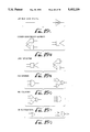
- an emulation system 10 in accordance with the present invention comprises a data entry workstation 12, at which a user enters information describing an electronic circuit or system which it is desired to emulate.
- Configuration information created by the data entry work station 12 is passed to a configuration unit 14.
- Configuration unit 14 contains the circuitry necessary to accomplish the programming of the programmable gate arrays (discussed more fully below) which are contained within an emulation module 16.
- Emulation module 16 includes a plurality of logic chips 18(a)-18(c) and a plurality of interconnect chips 20(a)-20(c) arranged in an array.
- emulation module 16 of FIG. 1 is shown having three logic chips 18(a) 18b and 18c and three interconnect chips 20a 20b and 20c.
- the emulation module will be discussed in more detail in section 1.3 below.
- the array size depicted in FIG. 1 is for illustration only and that, in an actual embodiment, the size of emulation module 16 is limited only by simple design choice.
- Data entry work station 12 may be a presently-available work station such as those manufactured by Daisy, Mentor, and Valid Logic.
- Data entry workstation 12 generates a description of the electronic circuit or system, e.g., a gate level netlist, from data input by a user in a manner well known in the art. Using several software programs, the operation of which will be described in detail in section 2 below, data entry workstation 12 produces a set of files necessary to program the interconnections and logic functions within each of the programmable gate array chips in emulation module 16, probing logic section 22, logic analyzer/pattern generator 24 and interface 26, which provides the connection to the user's external system 28 which is to work in conjunction with the emulated circuit.
- Configuration unit 14 then configures the system using the files produced by data entry workstation 12.
- Emulation array 16 includes provisions for connections to external VLSI devices 30 and external memory devices 32, which may thus be included in the circuit emulation performed by system 10.
- logic chips 18(a)-(c) The primary function of the logic chips 18(a)-(c) is to implement a large combination of logic circuit elements and is limited only by the available pin count and the integration capacity of the chips. Those of ordinary skill in the art will recognize that a large number of presently-available logic circuit kernels will function satisfactorily in the architecture of the present invention.
- logic chips 18(a)-c may be integrated circuits available from Xilinx of San Jose, Calif., (part Nos. XC3090, XC4005, and XC4013 are exemplary).
- interconnect chips 20(a)-(c) (which may be referred to herein also as mux chips of QT mux chips) is to provide connectivity between logic circuits in the logic modules 18(a)-c as well as to provide connectivity to signals originating outside of emulation array 16, such as signals originating in the user's external system 28, as well as external VLSI devices 30 and external memory devices 32 which may be part of the emulated design or may be included in the user's system which includes the emulated design.
- Each interconnect chip 20 acts as a crosspoint switch where each pin can be defined as either an input or an output, and each input can be connected to any output or group of outputs.
- the Xilinx XC3090 provides an interconnect capability which is satisfactory for the present invention.
- each interconnect chip 20 is connected by one or more conductors to each logic chip 18 and also has additional connections to external signals.
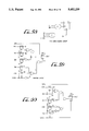
- the functionality of and interaction between logic chips 18(a)-(c) and interconnect chips 20a- c may be more easily seen with reference to FIG. 2.
- the emulation module 16 of the present invention is presented in somewhat more detail.
- a number of logic chips, 18(a)-(c) are connected to a number of interconnect chips 20(a)-(c), so that each logic chip makes one or more connections to each interconnect chip.
- logic chip 18(a) is shown connected to interconnect chip 20(a) by connections 40, to interconnect chip 20(b) by connections 42, and to interconnect chip 20(c) by connections 44.
- logic chip 18(b) is shown connected to interconnect chip 20(a) by connections 46, to interconnect chip 20(b) by connections 48, and to interconnect chip 20(c) by connections 50.
- Logic chip 18(c) is shown connected to interconnect chip 20(a) by connections 52, to interconnect chip 20(b) by connections 54, and to interconnect chip 20(c) by connections 56.
- the logic chip 18(a)-(c) may also have local interconnects; that is, each logic chip may have one or more of its pins connected to the pins of adjacent logic chips. This feature of the invention is illustrated by connections 58 and 60. While the use of an architecture including local interconnects is within the scope of the present invention, it may render certain designs placement sensitive.
- the logic and interconnect functionality may be implemented on a single chip.
- This implementation has the disadvantage that fewer I/O pins are available to connect to logic within the chip. Thus, less effective partitioning results.
- the number of conductors used to connect each logic chip 18 with each interconnect chip 20 may vary in any individual emulation system constructed in accordance with the present invention, and those of ordinary skill in the art will thus recognize that conductors 40-60 are symbolic and each may include one or more individual conductors.
- N the number of logic chips needed to attain the desired capacity
- P the number of pins available on each interconnect chip
- S the number of signals from each interconnect chip which must connect to external devices, including other emulation arrays
- C the number of conductors to use to connect between chips as dictated by the particular design.
- any logic chip 18 may be connected to any other logic chip 18 with only a single pass through an interconnect chip 20.
- the chip-to-chip delay is therefore both short and consistent throughout an emulated design.
- a frequent requirement for clock distribution is star routing, in which one signal connects to many logic chips. Implementation of such routing is simple and straightforward using the architecture of the present invention, and provides a uniform clock delay since one interconnect chip 20 connects to all logic chips 18.
- emulation modules 16a-c are connected together through interconnect chips 22(a)-(c). More specifically, emulation module 16a is interconnected to interconnect chips 22(a)-(c) via connections 68, 70, and 72, respectively.
- Emulation module 16b is interconnected to interconnect chips 22(a)-(c) via connections 74, 76, and 78, respectively.
- Emulation module 16c is interconnected to interconnect chips 22(a)-(c) via connections 80, 82, and 84, respectively.
- external VLSI devices 30 and external memory 32 may be connected to the circuit through one or more interconnect chips 22(a)-22(c) via connections 86 and 88, respectively.
- a single circuit board as just described may be thought of as a single logic chip, and a plurality of such circuit boards may be connected to one another by a plurality of interconnect chips to form an emulation array system.
- individual emulation systems may be thought of as individual logic chips 18 and may be connected together by use of interconnect chips.
- FIG. 2 By considering the architecture of FIG. 2 to be a single logic module (whether implemented as an integrated circuit or as a printed circuit board containing more than one integrated circuit) those of ordinary skill in the art will appreciate how the architecture of the present invention may be extended to the system level, thus allowing the construction of systems with arbitrary gate capacity.
- Rent's rule which is well known to those skilled in the art, is used to predict the number of external connections needed based upon the total amount of logic being implemented.
- the chip, board, and system boundaries do not necessarily match the architectural boundaries in the present invention. For example, it is possible to have two hierarchical levels within a single printed circuit board. This is not usually desirable, however, because the limited interconnect at each architectural boundary will constrain the placement of logic to be emulated. Fewer architectural boundaries will result in fewer constraints and a larger effective overall gate capacity.
- the emulation system 10 of the present invention utilizes a multiplexed (mux) interconnect architecture, wherein the chips comprising the emulation modules 16 are divided into two types: logic chips 18 and mux or interconnect chips 20.
- the logic chips 18 contain logic and generally do not provide any through routing.
- the mux chips 20 generally do not implement any logic; they generally implement routing.
- the circuit board traces may be multiplexed (switched) among many logic chips 18.
- Each logic chip pin (other than control pins) is wired to a mux chip 20 on the same emulation module 16 shown in FIG. 1.
- Each mux chip pin (other than control pins) is wired to a logic chip 18 or an external I/O.
- Each emulation module external I/O pin is also wired to a mux chip 20. (The special purpose I/O pins, control, programming, J-tag, etc., are handled separately).
- Each mux chip 20 has at least one connection to each logic chip 18 on the same emulation module 16. Thus, a signal can be routed from one logic chip 18 to any other logic chip 18 or to an external by passing through only one mux chip 20.
- each backplane mux chip 22 has several connections to each emulation module 16 and several connections to external pins. A signal is routed from one emulation module 16 to any other emulation module 16 or to an external I/O pin in just one hop.
- This scheme assumes that pods and component adapters allow arbitrary pin assignment, otherwise system routing becomes difficult.
- no backplane mux chip 22 will have more connections to any one pod or component adapter mux chip than it does to any emulation module 16.
- the hardware components of an emulation system 10 in accordance with the present invention are controlled through a a serial bus referred to as the PBUS (described below).
- the PBUS is routed through the backplane 24, providing access to all emulation modules 16, pods, component adapters, and a logic analyzer.
- the PBUS is tranformed into a standard VME BUS (not described) which is then connected to the workstation bus through a Bit 3 adapter available from Bit 3 Corporation of Minneapolis, Minn. Logically it is mapped into the workstation memory.
- the emulation module 16 of the present invention contains logic chips 18 and multiplexer chips 20 along with other logic.
- Preferred specifications are:
- the multiplexer chips 20 and logic chips 18 are surface mounted to the top of the emulation module board.
- the logic chips 18 alternate with multiplexer chips 20 as shown in FIG. 5.
- the layout shown is presently preferred for board routing.
- Emulation modules 16 are approximately 18.5" ⁇ 22". This is considered to be the largest size which fits current assembly equipment. External I/O is achieved through two high density 600 pin connectors on the front edge of the board. The connectors have 6 rows of pins on 0.1" ⁇ 0.1" centers and are approximately 9" long. Four connectors give a total available pinout of 2400 pins which is sufficient for power, ground, a VME bus, a programming bus, and the I/O signals. The connectors mate to the midplane as shown in FIGS. 6 and 7. There are no pod connectors on the emulation module 16. Pods connect to the multiplexed backplanes instead.
- circuitry on the emulation module includes:
- Programming Bus--A serial programming bus is used to transfer data inside the system, and each emulation module contains an interface.
- the programming bus also includes a JTAG test port.
- Test and Configuration Circuitry--Circuitry is provided so that all logic chips and all multiplexed chips can run both system interconnect and internal tests through the JTAG port.
- Clock Buffering Circuitry--Six low-skew clocks are provided.
- the clocks go to all logic chips in the system and also to the component adaptor and pod connectors.
- Special circuitry is provided to generate and buffer the clocks so that skew between boards and chips is kept to a minimum.
- the minimum number of emulation boards which are utilized in the emulation system 10 of the present invention is one, representing 30K gates.
- the maximum number is 11, representing 330K gates.
- each emulation board 16 has a capacity of 30K gates. This number is based on a total of 46 LCAs on each emulation board, with an average capacity of 652 gates per LCA.
- the emulation board 16 supports only 1,368 I/O pins on the backplane 24.
- Each mux board 26 (see FIG. 7) has 88 connections to any given emulation board 16.
- sixteen mux boards 26 are utilized per system. Note that in the preferred form sixteen mux boards 26 are always utilized for 30K emulation boards, no matter how many emulation boards are used in the system. This is a consequence of the midplane architecture (discussed more fully below).
- the LCA or logic chip 18 connectivity is designed for symmetry. This means that a design file for one LCA or logic chip 18 can be moved to any other LCA in the entire system, without totally reconfiguring the LCA. This greatly simplifies the placement software, because once a design has been partitioned into emulation boards 16, the placement no longer matters. Symmetry is achieved when the number of mux chips 20, connections per mux chip 20, and clock lines are all balanced to make all LCAs 18 look the same. Symmetry is also affected by the number of I/O pins on the LCA 18 and the QT mux chip 20.
- the system 10 of the present invention uses LCAs in 208 pin PQFP packages, with 144 I/O pins. It also uses QT mux chips in 208 pin PQFP packages with 168 I/O pins.
- the largest symmetry point which fits on the current emulation board form factor requires 46 LCAs 18 and 46 QT mux chips 20.
- Each LCA 18 has three connections to each QT mux chip 20.
- the remaining six LCA I/O pins are used for low skew signals.
- Those skilled in the art will recognize, however, that the number of LCA 18 and mux chips 20 and the number of connections between them is purely a design choice. A symmetric connectivity is not essential to the system, although it is desirable.
- QT mux chip connectivity is not symmetric. As shown in FIG. 4, QT mux chps MUXxx00 through MUXxx -- 05 are special in that they have two pins devoted to the global and local signals. This places some constraints on the router software, but the constraints are not serious.
- each mux chip 20 has three connections to each logic chip 18.
- the remaining 28 or 30 mux chip I/O pins are used for backplane I/O nets to the mux boards.
- the 40 regular and six special QT mux chips 20 represent 1,368 total connections to the mux boards.
- the system 10 of the present invention utilizes a midplane architecture, which removes QT mux chips 20 from the backplane and moves them to mux boards.
- the emulation boards and mux boards share many of the same physical pins on the backplane.
- the resulting connectivity is unusual, and affected by such things as connector pitch, number of connector rows and columns, and connector spacing.
- each emulation board/mux board intersection there are 96 pins.
- the emulation board uses an 12:1 interleave pattern for power/ground pins. This requires 8 pins from each intersection, leaving a total of 88 user I/O pins between any emulation board and any other mux board. Again, 1,368 I/O nets per emulation board, at 88 pins per mux board, requires a minimum of sixteen mux boards per system.
- the PBUS 30 which is discussed more fully below, is used to program and monitor all the LCAs and QT mux chips in the system, and to configure the low skew nets.
- the emulation board supports 44 PBUS signals which are described more fully in section 1.4.1 below.
- the interface to the PBUS is presently implemented using three Xilinx XC 3090 LCAs.
- This logic receives the PBUS data stream, and supplies two data streams to the emulation board: the LCA bit stream, and the JTAG bit stream. For efficiency, this logic should be the same design used on the mux board.
- the clock distribution network is shown in FIGS. 8 and 9.
- clocks are routed to the system board on the nets GLOB -- xx -- S -- 0:5. Clocks may be driven onto these nets from the emulation boards or the mux boards through the mux chips labelled MC 0:5.
- Each set of backplane nets is designed to have the same length to minimize skew.
- variable clock oscillator which provides clock signals to the emulated design if it is not being driven by an external clock.
- IOB192, IOB195 which are clocks provided by the internal pattern generator.
- RVE -- DS which is a clock provided by the RVE circuitry described later.
- Six BNC connectors are also provided on the system board which may be used to source or output signals to/from the clock nets.
- FIG. 9 shows how clocks are distributed on the emulation board.
- Clocks may be input either from the backplane through the GLOB -- S -- xx -- 0:5 signals or provided locally from the LOCALxx -- 0:5 signals.
- the upper four emulation board clock signals are multiplexed with JTAG signals TDO, TCK, TDI and TMS.
- the JTAG signals are used during testing of the FPGAs and board interconnect.
- a multiplexer is used to drive the LOSKEWxx -- 0:5 signals which go to the 46 LCAs 18 on the emulation board 16. There are actually additional buffers not shown in FIG. 9 to obtain sufficient current for driving all 46 LCAs.
- the main functions of the system board are:
- the porting of 160 channel logic analyzer from conventional systems is done by depopulating all unnecessary parts from the control board of those systems (for example, the RPM emulation system manufactured by Quickturn Systems of Mountain View, Calif.) converting the control board into a VME slave board and mounting it on the system board, with the required I/O and signal interfaces routed through this board.
- RVE is embedded in the present system 10 by mounting the control board of RVE directly on the system board, with all necessary control signals and vector channel signals routed through the system board.
- the RVE is a commercial product which may be purchased from Quickturn Systems of Mountain View, Calif., and is used when running the emulation system with test vectors.
- the host workstation 12 communicates with emulation board 10 through a bus extender card available from Bit-3 Corporation of Minneapolis, Minn. This drives a VME bus which again is converted into an internal bus called PBUS. This PBUS is then used to program all devices and set various control registers of all boards in the system.
- the logic to convert the 32 bit parallel VME bus data to serial PBUS data, latches to hold the PBUS address lines static while the bus performs some functions etc. will all reside in the system board.
- This board supports the Global lines routing scheme where the multiplexing of different sources of clocks (from/to Pods, BNCs, EMs, are handled. Also, there are a total of 12 BNC connectors on the board--two of which are from the 160 Channel LA/PG, another four from the RVE and the other six are for bringing in/out external clocks to system and routing them into the clock multiplexers.
- the PBUS is used for communication between the host or system board and emulation modules, mux boards and pods. Its primary functions are programming, readback and testing of LCAs 18 and mux chips 20. It may also be used for programming and reading back other registers in the system.
- the PBUS consists of a set of parallel address and control lines along with a set of serial data lines.
- Four different serial formats are supported; Register format for reading and writing board registers, LCA format for programming and reading back LCAs, JTAG-MUX format for programming and testing mux chips and for testing system interconnect and JTAG-LCA format for testing LCA to mux chip interconnect.
- the PBUS is synchronous with no ready or acknowledge line.
- the bus master is assumed to know what the acceptable data rate is for each slave device.
- the PBUS is a single master bus. There is no facility for switching the bus master. The system board located in slot 38 will automatically become the bus master. Other system boards will be PBUS slaves. Physically, the PBUS is split into two halves to keep the length and loading reasonable. One half goes to connectors in the mux board side of the cardcage and the other half goes to connectors in the emulation module side of the cardcage.
- the address portion of the PBUS contains 16 address signals SB -- xx -- PA0:15 which select an individual board and chip for programming, readback or testing.
- SB -- xx -- PA0 is the least significant bit.
- the address field is partitioned as shown:
- Address Type is one of the following:
- Register address--Used when reading or writing control registers on boards attached to the PBUS are also used when the system is emulating the user design. Note that some registers on the VME to PBUS interface logic are attached directly to the VME bus, rather than to the PBUS.
- LCA address--Used to program or readback LCAs An LCA address may not be given when the user design is emulating because the DIN pin on LCAs is also used as a global clock and is switched to the data-in function whenever an LCA address is selected. Once an LCA address is selected and programming or readback is started, the address must not be changed until the program or readback operation is complete. Otherwise, the program or readback operation will not complete correctly and there is a possibility of the part being damaged due to a bad bitstream.
- JTAG -- MUX addresses may be used while the user design is emulating. This is necessary to determine the source and pin number of I/O conflict interrupts. Mux chip addresses should only be changed when the mux chips are in the TEST-LOGIC-RESET or RUN-TEST-IDLE states. TMS is either held constant or forced high for unselected mux chips.
- the low-skew clock lines are redefined to be JTAG control lines.
- LCAs 18 must be programmed with a JTAG bitstream before selecting this address type and erased afterwards to avoid conflicts on the low-skew lines.
- the low-skew clock register must be reinitialized before the user's design will run.
- LCA chip addresses should only be changed when the LCA chips are in the TEST-LOGIC-RESET or RUN-TEST-IDLE states. PTMS is either held constant or forced high for unselected chips.
- the top bit of the board address field will be used to select between mux board connectors and emulation module connectors in the system. This is only an addressing difference; it does not imply anything about the board type.
- the emulation module connector will accept several different types of boards.
- the device address field is used to select a particular LCA 18, mux chip 20 or register. It may be further subdivided on some boards. On mux boards, part of the device field is used to select different I/O connectors.
- Boards may have hard-programmed LCAs as well as user-programmed devices.
- the emulation module 16 will use several LCAs for the PBUS interface and programming address decoder. These devices may have diagnostic readback addresses which should be located at the top of the device address space.
- Global addressing can be used for parallel programming all LCAs or all mux chips in a system or on a board. It is also possible to test all mux chips on a board or in the system in parallel. Global addressing does not support specific board types. For example, it is possible to program all mux chips in the system or all mux chips on mux board 5 but not all mux chips on all mux boards or all LCAs in pods.
- PA14,15 determine whether LCAs or mux chips are accessed with a global address. On I/O connectors, only 4 bits of the device address appear on the connector. The global device address becomes:
- the slot ID signals are compared to the board address portion of the PA address to determine if a particular board has been selected. Slot ID signals are connected to ground or left unconnected on the backplane to uniquely identify a board slot. The slot ID signals will have pullups on each board.
- Mux boards will have slot identifications of 00H to 17H (0-23 decimal) and emulation modules will have slot IDs of 20H to 2BH (32 to 43 decimals).
- the master system board must reside in slot 26H (38 decimal). This is the board that drives the PBUS.
- SB -- xx -- ID5 is a 1 for boards on the emulation module side of the cardcage and a 0 for boards on the mux side of the cardcage.
- Signal type is defined with respect to the emulation and mux boards.
- I is an input to the board
- T is a tristate output
- OC is an open-collector output with a pullup on the backplane.
- Some of the controls signals have different functions when JTAG or LCA addresses are selected.
- PTDI, PTMS and PSYNC-- are valid before the rising edge of PTCK and PTDO and PINT-- change after the falling edge. Address is changed only when PTCK is in the high state.
- PTCK is decoded on each board into separate clocks for mux chips, LCAs and LCAs in JTAG mode and goes to all devices of a given type. This is like the CPU board today but unlike the current emulation module.
- the PBUS interface will automatically load array LCAs with a blank bitstream file known as "empty.bit" during the bootup process.
- I/O connectors have individually decoded PTCKs and are not loaded with empty.bit during the bootup process. This allows the system to recover gracefully if pods or CA cards are removed and replaced while an emulation is in progress.
- PTCK will stop in the high state when the host CPU is fetching new data or when no operations are in progress. Excess clocks after programming or readback is complete are ignored by registers, LCAs and mux chips.
- the PTDI signal When generating a strobe for LCA program or readback, the PTDI signal is used to select between the Done/Program pin (program LCA) and the M0 pin (readback LCA).
- a 0 level means program and a 1 level means readback.
- the same encoding scheme is used in the current pod.
- SB -- xx -- PTMS--Model select signal in JTAG mode for the JTAG logic in mux chips or LCAs.
- PTMS is sampled on the rising edge of PTCK.
- PTMS is decoded so that it only goes to the device(s) selected. For unselected devices, it either remains high or remains in the last selected state depending on a bit in the board control register.
- JTAG testing it is necessary to write data to some chips and have them remain in the EXTERNAL-TEST state while reading data from other chips. This is done by placing unselected chips in the RUN-TEST-IDLE state with PTMS low.
- Many mux chips may be operated in parallel by selecting one of the global addresses and placing the appropriate 1/0 pattern on the TMS signal. This technique can be used to do an internal test on all mux chips in the system in parallel.
- the PTMS signal When an LCA program/readback address is selected, the PTMS signal becomes an active-low global LCA reset. It is used to reset LCAs before reprogramming or before starting emulation. This reset will not affect the configuration of LCAs.
- the PTMS signal When a register address is selected, the PTMS signal becomes the active-low write enable signal. If PTMS is low, register contents will be changed to reflect the data input on TDI. If PTMS is high, register contents will be read out but not changed. Register contents may change one bit at a time or all together depending on the particular register. Unmodified register bits will not toggle during the writing process, however.
- SB -- xx -- PRST--PRST- is a reset for all boards attached to the PBUS. It operates similar to the VME bus reset signal and a VME reset will also cause a PBUS reset.
- PRST- causes all hard-programmed LCAs to reprogram and all interface logic to reset. It has the same effect as power-cycling the interface logic. It is not the same as the user design reset which is done by placing a 0 on PTMS while giving an LCA address.
- SB -- xx -- PSYNC--PSYNC- is an active-low synchronization signal for register reads and writes. It pulses low to reset the bit counters before data is shifted in or out of the register.
- PSYNC- is used to generate the D/P or M0 strobes.
- the PTDI signal determines whether a D/P (program) or M0 (readback) strobe is generated.
- the PSYNC- signal is used to clear the TDO comparison latch before starting a mux chip internal test.
- Typical PBUS Waveforms are Illustrated in FIGS. 83-85
- FIG. 83 An example of an 8 bit register read/write operation is shown in FIG. 83.
- the PSYNC- signal clears an internal bit counter. The counter increments until it reaches 8 then it stops. Further clocks have no effect.
- TDI data is sampled by the rising edge of PTCK and TDO data changes on the falling edge.
- the TMS signal is used as a write enable.
- LCA program and readback have similar waveforms.
- the PSYNC- pulse is wider and there are more clocks but the timing is the same.
- Input data is sampled on the rising edge of PTCK and output data changes on the falling edge of PTCK.
- JTAG format again, has similar timing as shown in FIG. 100.
- PTDI and PTMS change after the falling edge of PTCK and are sampled by the rising edge.
- PTDO changes after the falling edge of PTCK.
- the mux board is a PC board that is long and narrow, with five system I/O connectors on one edge.
- the mux board plugs into the system backplane 24.
- the mux board has ten QT mux ICs mounted thereon.
- Each QT mux IC has 168 programmable I/O, and is able to switch any incoming signal onto any other outgoing signal (either back to some other emulation module 16 or to the outside world).
- the programming of the mux ICs is done through the backplane PBUS from the system board, and the VMEbus is not used on this board.
- a minimum of sixteen mux boards are plugged into each backplane connector slot (on the mux side of the backplane, not the emulation module side).
- a maximum of 24 can be plugged into the backplane, and the system emulation capacity can be expanded to a theoretical limit of around 500,000 gates (as per Rent's rule).
- the mux ICs are configured through the PBUS entering the mux board from the backplane 24, as per the addressing scheme given in the discussion of the PBUS in section 1.4.2 above.
- Emulation boards and the system board are connected together through a switching midplane.
- the switching midplane is more fully disclosed in co-pending U.S. patent application Ser. No. 07/896,068, filed Jun. 8, 1992, and entitled "SWITCHING MIDPLANE AND INTERCONNECTION SYSTEM FOR INTERCONNECTING LARGE NUMBERS OF SIGNALS".
- the switching midplane includes a midplane printed circuit board with connectors on one side for the emulation modules and system board and connectors on the other side for the mux boards. The connectors are oriented at right angles to each other such that each mux board connects to the system board and all the emulation modules. This is illustrated in FIG. 7.
- the combination of the midplane circuit board and mux boards comprises the switching midplane.
- the switching midplane allows signals to be routed from any emulation module to another emulation module, the system board, or an I/O connector with only one pass through a mux chip.
- the multiplexer chip 20 has a large number of bidirectional I/O pins. Any pin can be defined as an input, output, or bidirectional.
- the chip acts like a large crosspoint switch. Any input can be connected to any output or any group of outputs. It is possible for one input to drive up to half of the other pins on the chip.
- I/O pins and connection patterns are defined by loading a serial configuration pattern into static RAM inside the chip.
- the chip is statically non-blocking. For any pattern of inputs and outputs, there is a configuration pattern which will make the desired connections. Internally, the chip is a large crosspoint switch where each configuration bit causes a connection between an input pin and an output pin.
- the multiplexer chip 20 may also serve as a wired and bus extender. In this case, multiple inputs are tied together through a pulldown bus which is then routed to an output pin. Multiplexer chips may be arranged in a hierarchy to propagate buses throughout the system 10.
- mux chips are used in 3 distinct places, each of which has slightly different characteristics.
- Mux chips 20 have a number of connections to each logic chip 18 and a number of additional connections to the backplane connector. All connections are static. There are no bidirectional or tristate signals. CMOS input levels are used for all pins. A single input may fan out to approximately 46 outputs. It is possible for all pins to switch simultaneously, at least in a localized area of the chip. Outputs drive one CMOS input and may have up to 3 feet of trace with a typical impedance of 50-75 Ohms.
- 76 Pins connect to the system through the I/O connector. 76 additional pins are available for connection to a user design. These pins can be used in various ways. Up to 38 of them can be bidirectional with separate enables or more if enables can be shared. Up to 76 pins can be static inputs or outputs.
- the mux chip includes a JTAG port which is used for testing and configuration.
- the JTAG port follows the IEEE 1149.1 specification. There are 4 JTAG pins with the following functions:
- TCK--Clock input used for shifting data and changing the JTAG mode.
- TCK also provides a clock for the error detection logic and is expected to run continuously while the design is emulating.
- TDI and TMS are sampled on the rising edge of TCK and TDO changes on the falling edge.
- TCK is common to all chips in the system.
- TMS--Test mode select pin which is toggled up and down along with TCK to change the current test mode.
- TMS is left at a 1 in the default or reset state.
- TMS is decoded to select one mux chip in the system.
- TDI--TDI is the data input for configuration and test data. TDI is common to all chips in the system.
- TDO--TDO is the data output for test data. It is also used to output configuration data to the next chip when chips are daisy-chained together. TDO is a tristate output. Only the chip actively shifting data drives TDO.
- the JTAG logic is composed of an instruction register and a series of data registers.
- the instruction register has 4 bits and selects the test or configuration mode. The following codes are used:
- the instruction register When read back, the instruction register contains program and I/O error status bits.
- the serial and parallel configuration modes are described in detail in the configuration section.
- the bypass register is a 1 bit register which is selected by default when none of the other modes are active.
- the bypass register is used to reduce test time when daisy-chaining many chips together.
- the external and internal test modes are described below.
- the serial programming mode is selected by writing the appropriate address to the JTAG instruction register when the part is placed in the SHIFT DR state and the programming data is shifted in. Outputs will be tristated as soon as the part is placed in the SHIFT DR state and will remain tristated until programming is complete.
- the open collector DONE output will be pulled low at power up and as long as the part is not programmed. When reprogramming, DONE will go low before the outputs are tristated and remain low until programming is complete and the outputs are enabled again.
- the chip will come up in the unprogrammed state with all outputs and internal drivers tristated and the JTAG logic in the Test-Logic-Reset state.
- a status bit is available in the instruction register which allows the CPU to determine that the part has not been programmed.
- the part can also be programmed in a non-JTAG environment by pulling the PGM/pin low then clocking configuration data in on TDI along with a clock on TCK.
- the mux chip may be booted from a Xilinx 3000 or 4000 series part and placed in a daisy-chain with other mux chips or Xilinx parts.
- a serial configuration pattern is used to load the mux chip.
- the format is similar to that used for a Xilinx 4000 series chip and is compatible in the sense that Xilinx 3000 or 4000 chips and mux chips may be daisy-chained together and loaded using a Xilinx chip as the master.
- the configuration pattern is composed of a header followed by a series of data frames. Each data frame starts with a 0 followed by 168 data bits followed by 4 bits of CRC check. The chip requires 256 data frames.
- a parallel programming mode is also supported to make chip testing possible.
- the parallel programming mode allows the part to be completely programmed in approximately 300 clocks instead of 43,000 clocks for the serial mode.
- a complete frame minus the start bit and the CRC check bits is placed on all the I/O pins at the same time. There is no start or stop sequence.
- the part is placed in the parallel programming mode by writing to the JTAG instruction register then moving to the SHIFT DR state.
- the TDI pin is held low until the last frame is entered then set high. If TDI is set high before configuration is complete or the JTAG logic is moved out of the SHIFT DR state, configuration will be aborted. With each clock, a new frame of data is written. The order of data frames is reversed in this mode.
- I/O pins have either 2 or 3 connections to the switching matrix. These are the input, output and output enable. Each output or output enable may be connected to any input or any combination of inputs. Any number of outputs may be connected to one input. This provides a fanout capability which is useful for distributing clocks. Outputs and output enables may also be configured to be a constant 1 or 0. If no input connections are programmed, the output or output enable will be a constant 1. If the cell in a diagonal location is programmed it will cause the output or output enable to be a constant 0. This cell would normally connect a pin back to itself which is not a useful function.
- Each I/O pin may be defined at configuration time as an input, output, bidirectional, open collector or open emitter by setting the I/O register and the output and output enable appropriately.
- a board in the system 10 will have approximately 8,000 wires which may have lengths from a few inches to many feet. Reflections, crosstalk and ground bounce must be tightly controlled but there is no room to add extra termination resistors or discrete buffers. Since there is no fixed signal definition, there may be many signals switching at once and clock and data signals may be intermixed.
- Normal outputs drive a PC board and/or cable with 50-75 Ohm impedance connected to exactly one CMOS input pin. There is no requirement for large amounts of DC current since normal outputs only drive CMOS inputs on other chips.
- I/O pins are individually selectable for CMOS or TTL input levels. Outputs are always CMOS levels. CMOS mode is intended for pins that must communicate with standard CMOS or logic such as Xilinx chips or AC parts. TTL mode is for external I/O on component adaptors or buffer pods. Only CMOS input levels are needed on configuration and test pins.
- Outputs are able to withstand a short circuit of unlimited duration so the part is tolerant of programming errors in the system and shorts in the plug hardware. This is achieved by incorporating error detection logic into the I/O buffer.
- a slow error clock is provided. If the output is trying to drive low and is above 0.8 V or is trying to drive high and is below 2 V continuously for a time equal to the slow error time period, the error detection logic will be triggered and the strong driver on the pin will be turned off. A parallel weak driver will remain enabled so the pin will recover when the short has been removed. The strong driver will only be turned off on the pin(s) which have experienced an I/O protection error. Drivers on other pins will remain enabled.
- the IOERR/line When an I/O error has been detected, the IOERR/line will go low. The user may use this signal to trigger an oscilloscope or logic analyzer. Software can determine which pin caused an I/O error by reading back the data register in the external test mode. Reading back the register will clear the error status and reset the error detection logic. The IOEER status bit can also be polled in the instruction register.
- FIGS. 13-15 The flow of the configuration process is illustrated in FIGS. 13-15.
- the parser 100 reads the user's netlists and interfaces with the downstream part of the configuration system through a public procedural interface.
- the link and expand module 102 links the netlist with the component libraries and then flattens the design description.
- the optimizer 104 transforms the logic for better implementation in the system hardware. In general it handles all transformations more complex than simple library element replacement. Its goals are improved clocking (mainly through blasting of inverters, removing buffers in the clock path and transforming gated clock logic to datapath logic), improved capacity, and implementation of structures (such as tri-state signals or bus retainers) that cannot be implemented well, or at all, with library elements.
- the optimizer module 104 There are two parts to the optimizer module 104: a framework for handling differences between the user's netlist and the implemented logic, and a set of transformations.
- the difference handling framework provides utilities for applying logic transformations and for mapping between the user's signals and gates and the implemented signals and gates. This is used both in interpreting directions from the user (e.g. TA net exclusion or incremental changes), and in returning reports to the user.
- the clock analysis module 106 finds clock trees and decides how the nets on the clock tree should be implemented. Large nets are placed on low-skew hardware, the smaller clock nets are routed on the regular interconnect but are given higher priority in the system partitioner 108 and in the chip placer and router 112.
- the partition module 108 partitions the logic into emulation modules and logic (Xilinx) chips.
- the user can influence this. He can specify that certain of his blocks be kept together on an emulation module or logic chip. Even without any such directives, the partitioner may try to use or preserve the user's netlist partitioning, both to speed up partitioning and to reduce the extent of incremental changes.
- the system router 110 assigns system level nets to specific multiplexed chips. The effect of this is to assign nets to specific chip pins.
- the chip place and route module can swap chip pins that connect to the same mux chip.
- the chip place and route module (CPR) 112 produces bit streams and delay data at an individual chip level.
- the timing analysis module 114 finds hold time violations, the maximum emulation speed, and path delays. Timing analysis is hierarchical. First, a chip level timing analysis is performed. Then splice the chip level results are spliced together to produce a design level analysis. This increases the speed of the timing analysis (TA) by splattering it across the network. It also speeds up timing analysis of incremental changes because only the chips that have changed are re-analyzed.
- TA timing analysis
- the delay insertion module 116 fixes hold violations through insertion of delay elements.
- partition module 108 the system router 110, and the chip place and route module 112 are comprised within the Timing Driven Configuration Engine 120 shown in FIG. 13.
- the configuration database contains all the data produced by the configuration system. Some of the configuration database, the part describing the input netlist, is used by both the configuration system and the user interface. Most of it will only be used by the configuration system.
- Access requirements are different for different parts of the database.
- the system partitioner iterates through its data thousands or hundreds of thousands of times to perform its task. Access to individual elements must be very fast, on the order of a few machine instructions, but relatively long open times to the system partition part of the database can be tolerated.
- the user interface accesses the configuration database to validate names entered by the user and to translate names between internal and external formats.
- Interactive access times are needed to individual objects--hundreds of milliseconds per access, but all of the names are generally not accessed during one session. However fast open times are preferred.
- the chip level placement and timing data has access requirements between these two extremes. This data is accessed on a per chip basis. All the chip level place and route data or all the timing data for one chip is accumulated and shipped off to the chip place and route module 112 or the timing analysis module 114.
- the netlist comparison module 118 accesses stored descriptions of the user's original blocks. These are accessed by blocks. A mapping from this hierarchical description to the flattened system configuration database is maintained.
- the configuration database may be organized in three or four sections: name 122, netlist 124, system place and route 126, and chip 128. (The name and netlist sections may be combined).
- the name database 122 stores the user's netlist. It assigns short internal ID's for signal and pin instances. It supports searching on signal and pin names and mapping between user names and internal ID's.
- the netlist database 124 is implemented as a random access database.
- the netlist database 124 describes the user's hierarchical netlist and the mapping to the flattened netlist. It is accessed by block during incremental netlist comparison.
- the system place and route database 126 describes the flattened netlist and which chip or chips will hold each of the elements in the netlist. It is read entirely into virtual memory when it is opened. Thereafter access is directly from virtual memory. To minimize the swap space and swapping required, the system place and route database 126 is made as small as possible. It contains no more than is necessary for system partitioning and routing, and references to the other sections of the configuration database.
- the chip database 128 describes the detailed configuration and timing of each chip. It contains bitstreams and enough other data to allow incremental changes. It is randomly accessed by chip place and route module 112 and by the timing analysis module 114. It supports access to all the place and route module or all the timing data for one chip with one call. It is mid-way between the netlist and system place and route databases in organization and performance.
- a problem inherent in emulation is that delays do not scale from the user's target technology to the emulation. This is particularly true for routing delays.
- a net that has only a few nanoseconds delay in the target technology may have anywhere from 0 to about 150 ns. delay in the emulation system 10.
- the average emulated path has more routing delay than gate delay.
- the worst paths have much more routing delay than gate delay.
- a path that is emulated in one logic chip will be quite fast; one that jumps from chip to chip or, worse, board to board will be quite slow.
- the variation in routing delay between different paths is quite high, even if the paths have the same amount of logic. The opposite is true in most target technologies.
- Hold violations occur because of skew in a clock tree.
- Set-up violations occur because one of the datapaths has a large amount of delay, generally routing delay.
- Timing problems are created primarily in the system partitioner 106 and in the chip level place and route system 112 and, once created, timing problems can be difficult to solve.
- the system router 110 does not affect timing unless it is allowed to split a source onto two or more chip pins. All chip to chip routes have the same delay and all board to board routes have the same delay (except for variations between individual mux chips). Because it is preferred that each configuration work with any emulation module, worst case mux chip timings are assumed. If the system router splits a source onto two or more chip pins then the system level router will increase the skew on the net.
- the configuration software of the present invention is directed to avoid hold violations.
- the optimizer 104 removes buffers and inverters from the clock tree (and all other paths) and transforms gated clock logic from a clock path and adds it to a datapath when possible.
- the clock tree analyzer 106 extracts and analyzes the clock tree before partitioning. It decides which clock nets to route on low skew hardware and directs the system partitioner 106 and chip place and route module 112 to reduce delays on the rest of the clock nets. If the system level router 110 is allowed to split source pins it will be told not to do so on the clock tree. This eliminates hold violations unless the design has a very complicated clock tree.
- delay insertion When a clock tree is complex, hold violations are eliminated through delay insertion. Delay is generally inserted after the initial configuration. For example, when the timing analyzer 114 finds hold violations, it estimates their magnitude, and delay elements are inserted incrementally.
- Emulation speed is improved by reducing system level interconnect delay on the critical paths. This is achieved by using timing driven partitioning algorithms.
- One of the ways to cause the partitioner 106 to prevent a certain net from being cut is to give that net a higher weight. However, if this mechanism is used on too many nets, the effect on the quality of the partition may become unpredictable or it may become ineffective altogether. Also, for timing purposes, it is the path that is important, not the net itself. Timing driven partitioning attempts to find the critical paths and uses cone based partitioning and path based clustering algorithms to reduce the delays on critical paths.
- timing driven partitioning generates delay budgets to FPGA chip level placement and routing along the critical path portion of the datapaths. By doing this, delays on the critical path can be further reduced.
- the goal of incremental mode is to quickly change the configuration in response to small changes in the input. It must also preserve the timing of the emulation as much as possible.
- a change record is of the form "delete object” or "add object”.
- Change records are generated by the user interface when a probe or pod is changed, or by the parser 100 when the netlist is changed.
- the set is then moved through the modules of the configuration system. As the set moves through the system the change records are transformed, both in quantity and type. Initially the change records refer to logical objects in the input netlist. When they get to chip level place and route they refer to specific gates and nets in particular chips.
- Incremental configuration uses one module not used in the initial configuration, a netlist comparison module 118.
- the parser 100 detects massive changes to a block or netlist file it simply issues a delete record for the whole netlist block or file and issues add records for the objects in the new version.
- the netlist comparison module 118 is then called to compare the old and new versions. It performs a graph comparison, ignoring all signal and instance names inside the changed object.
- the netlist comparison procedure generates change records with a finer granularity.
- each module should retain the mapping between its input and output so that it can translate delete records properly.
- the parser module 100 is of conventional design and its function is believed to be well-known in the art. For this reason, the function of the parser module 100 will be described only generally.
- the parser 100 accesses the user netlist and the CAE database (which comprises a number of vendor libraries) and generates a netlist connectivity database 124.
- the netlist connectivity database 124 comprises a representation of the circuit design to be emulated in hierarchical form (i.e. repeated subportions of a circuit to be emulated are described only once, but may be referenced as many times as necessary).
- the parser 100 transforms a "human-readable" description of the circuit to be emulated into a "machine-readable” circuit representation.
- the purpose of the component library linker is to assist the netlist parser in linking undefined components in the netlist to their actual definition which had been stored in a linkable vendor-specific component library.
- the linker 102 is invoked by the parser 100 at the end of the parsing phase to fill in all undefined netlist components definitions. For each of a undefined netlist component the linker is given the component name and the list of component pins. It is assumed that all the undefined components can be located inside the IC vendor-specific component library which is being used to implement the particular netlist design. The linker gives an error message when undefined components cannot be located in the component library.
- the linker currently has to provide in-memory NTL to the link and expand module 102 data structure conversion since component libraries generally use NTL data structure and the parser uses the link and expand module 102 data structure.
- a hard-coded list of Xilinx primitives is used by the linker to avoid expanding lowest level components.
- Netlist expansion and tree construction software is the front end of the system internal configurer (QBIC). It is treated here as a separate piece of software, although the software is linked in as part of QBIC.
- the netlist expansion software is named ELO which stands for Expand, Link and Optimize. However, the software currently does not perform linking and optimization.
- ELO ELO data structure built by the parser 100
- QBIC tree QBIC tree
- FIG. 15(a) shows the system box configuration flow.
- the parser 100 parses the user's netlist and creates a run time ELO data structure.
- the link and expand module 102 expands the data structure and constructs the QBIC tree which is used by the system place and route module 110.
- the parser 100 generates the link and expand module 102 structure for the modified portion of the design, and the link and expand module 102 updates the QBIC tree and generates a list of changes for the system router 110.
- the link and expand module 102 receives from the parser 100 a list of block definitions (ELO block record).
- a block record may describe a primitive or a high level component. It has a list of external pins, a list of internal components, and a list of nets describing how the internal components and the external pins are connected.
- a block record is independent of other block records; that is, a block record contains the complete information describing itself. This list of block records is used to form the QBIC tree.
- the QBIC tree is a fully initiated netlist tree where each block reference in the netlist is replaced by a node; that is, every block has one copy in the tree for each initiation in the netlist.
- the QBIC tree is the primary data structure for the system place and route module 110, CLB mapping system (CMS), and others. The leaves of the tree must be CLB mappable.
- the component list and the netlist within an ELO block record are sorted into alphabetical order in order to ensure efficient comparison during incremental change detection.
- the pin list for an ELO block is not sorted currently, but it may be preferred to sort the list in the future.
- ELO data structure and QBIC tree are glop-dumped together since ELO data structure and QBIC tree are linked together.
- Expansion is a simple, recursive process: for a given component, find a netlist description for the component's contents. If there is such a description, add the description to the tree, then recursively descend into the components which were added.
- the principal work done is (a) pin resolution--matching up the net connected to a pin on the outside of a component with the net connected to the corresponding pin on the inside; and (b) addition of contents (nets and components). This correlates loosely to a macro expansion, where pin resolution is analogous to argument substitution.
- ELO divides this into two modules.
- the traversal module which finds the internal descriptions and does the recursive scan of components, relies on the handler module to build the tree.
- the handler module provides an abstract interface so that the traversal module has limited knowledge of the tree being built.
- Each time the traversal module encounters a component it calls a routine to add the component to the tree, and each time it gets a list of nets, it must be added to the tree. Then, if the current component has netlist contents, the traversal module does pin mapping (setting special correspondence pointers to allow a net in the netlist to figure out what it connects to outside the component) and calls itself recursively.
- Umbilicals and hard-cards are treated in a special way, so that the system place and route module 110 can handle them earlier in the partitioning process.
- the link and expand module 102 currently constructs special lists to umbilicals and hard-cards in such a way that QBIC tree is not disturbed; disturbing the tree would cause a good deal of difficulty in incremental update.
- Incremental change detection is done by a piece-by-piece comparison of the changed data versus the original tree.
- the changed block definitions are compared against all of their initiations in the tree.
- the link and expand module 102 patches directly to the tree and supplies QBIC with a list of changes made.
- .ELO keeps track of all the block types that are used..82 The list is ordered according to the maximum depth at which a type appears in QBIC tree. Traversing this list, ELO safely visits each node to update before any of its children.
- Memory usage for this system is roughly linear, at 0.6 megabyte per kGate for tree construction, and 0.6 mb per Kgate of changed clocks for incremental change.
- a gate is not a "gate-equivalent", but is a leaf in the tree before CLB conversion. Thus, about one CLB for each four-five gates is expected after conversion.
- a flip-flop is considered a gate, as is any AND/OR/XOR gate which does not have more inputs than can enter a single CLB.
- the performance estimate includes only QBIC tree, excluding the expand the data structure.
- the run time complexity is nonlinear: for SPARC design, which has an 8 Kgate (2000 CLB), it comes out to be roughly 85 seconds of Sun 3/60 CPU time for tree construction.
- the link and expand module 102 receives the list of probe signals. Using the list, the link and expand module 102 marks those signals, and CLB mapping subsystem (CMS) ensures those signals are not embedded in CLBs.
- CMS CLB mapping subsystem
- the link and expand module 102 also marks all the bidirectional signals for system place and route system place and route handles those signals specially.
- the logic optimization module 104 OPT takes a netlist produced by the expand and link module 102, and produces an optimized netlist to be given to the system partitioner 108.
- the optimization module 104 takes change records for the unoptimized netlist, and produces change records for the optimized netlist.
- the optimization module 104 provides utilities for translating net grouping and exclusion and path delay query requests from the original netlist to the optimized netlist and for translating timing analysis reports from the optimized netlist to the original netlist.
- the optimization module 104 has a special mode in which it reads a file of commands generated by downstream software. The commands specify modifications of the current optimized netlist. After reading the file, the optimization module 104 modifies the netlist and generates a list of change records. The list of change records can then be processed by the downstream software.
- the logic optimization subsystem provides support for automatic hold violation correction.
- Logic optimization increases the variety of constructs which can be supported in user netlists.
- the retain-state bus optimization allows a user to specify a retain-state bus simply by attaching a "retain state" property to a net with tristate drivers.
- the logic optimization subsystem provides a uniform framework for allowing a physically implemented netlist to differ from the user's netlist. For example, logic optimization includes low-skew clock splitting, where a special "beefy buffer" is inserted in a low-skew clock net, splitting in into two sets.
- the optimization software module 104 is written assuming the simplest possible control flow:
- This scheme splatters most of optimization, saving time and some memory space.
- a third scheme is as follows:
- Parse and expand generating a top netlist, and a subnetlist for each user file
- An important objective of this scheme is to support "modular compile”: configuration produces a chip set for each board-size piece; when the user changes a file, only the chip set for that file's board needs to be processed.
- the first scheme with optimization before partitioning is preferred.
- the optimization module 104 has special modes in which it reads a file of commands generated by downstream software. The commands specify modifications of the current optimized netlist. After reading the file, the optimization module 104 modifies the netlist and generates a list of change records. The list of change records can then be processed by the downstream software.
- the timing analyzer is run and a file of (instance name, delay) pairs for hold-violation correction is generated. If corrections are needed, the optimization module 104 is then called in a special delay insertion mode. In this mode, the optimization module 104 reads the file and makes the requested changes in the current optimized netlist. Then the netlist is incrementally reconfigured. The process continues until no more corrections are needed.
- the optimization module 104 When called in delay insertion mode, the optimization module 104 expects a file named autodelay in the qtd directory containing entries of the form:
- block name is the instance name of a D latch or D flip-flop in the optimized netlist
- number -- of -- delays is the number of qt -- delay blocks to be inserted in front of the D input of the latch or flip-flop.
- the optimization module 104 reads the file, modifies the netlist (treating the changes as further optimizations), builds a list of change records, and returns. At this point the downstream software can be called in the normal way for an incremental configuration.
- AND-Tree optimization is performed by collapsing any AND-trees into single large AND gates, and replacing each AND-gate by a structure consisting of a (non-blastable) buffer for each input, a net with a "Wire-AND” property, and an output buffer. System partitioning and routing is then done. After routing, an "AND-finder" routine analyzes the router's data structures and produces a file named andtree in the qtd directory containing entries of the form
- net is the instance name of a Wire-AND net
- expr is an expression describing the AND-tree which should replace the net and its input and output buffers.
- the expression is built according to the grammar. ##EQU1## where each b is the instance name of a block driving the original AND, each c is the name of a (logic or mux) chip, and each cp is the name of a (logic or mux) chippin.
- DRIV[c,cp](b) describes block b on chip c whose output is connected to chip pin cp (possibly null).
- AND[c,cp](exprlist) describes an AND gate on logic chip c whose output is connected to chip pin cp (possibly null), and whose drivers are described by exprlist.
- a non-empty muxlist is used when the output of a driver block or AND gate is fed through one or more mux chips (without further ANDing) to another logic chip.
- optimization module 104 After AND-finder has produced the file just described, the optimization module 104 is called in a special Wire-AND-removal mode. When called in this mode, optimization module 104 reads the file and removes the Wire-AND net and the input and output buffers, replacing them with an AND-tree. It treats these changes as further optimizations in the netlist. It annotates each AND block, and each block that was driving the original AND, with the appropriate list of values [c, cp, . . . ]. It builds a list of change records for the netlist changes it has made and returns.
- the system place and route module 112 is called in wire-AND-removal mode.
- the system place and route module 112 takes the list of change records, reads the c,cp, . . . ]attributes describing the placement of each block and the routing of its output net, and fills in the appropriate fields in the netlist data structures.
- the wire-AND net in the netlist is replaced by an ordinary AND-tree.+ But only the optimization module 104 is allowed to make netlist modifications.
- the place-and-route data fields of the newly created netlist are updated. But only the system place and route module 112 is allowed to update these fields.
- the input data for the optimization module 104 consists of
- netlist data including connectivity, block types, block and net pathnames, net weights and net low-skewness.
- the netlist data can be represented using the following data types and attributes.
- T1>T2 A many-to-one relationship from type T1 to type T2 is written T1>T2. Such a relationship assigns to a given T1 object at most one T2 object, The operations normally needed are (1) given a T1 object, find its T2 object (if any), (2) given a T2 object, visit each of its T1 objects. If these are the operations needed, then a reasonable implementation is to have each T1 object have a pointer to its T2 object, and have each T2 object have a pointer to its first T1 object, with a thread in the T1 objects linking the T1 objects of a given T2 object in a list (perhaps a circular list).
- variable-length array for the T1 objects associated with a given T2 object. (This allows the thread pointers in the T1 objects to be eliminated). If one needs to rapidly get from a T2 object to its T1 object of a given name, one can replace the pointer from a T2 object to its first T1 object by a pointer to a hash table containing pointers to T1 objects. In this case, instead of having a thread linking all the T1 objects of a given T2 object, we have a thread linking the T1 objects of a given bucket.
- T1 ⁇ T2 A one-to-one relationship from type T1 to type T2 is written T1 ⁇ T2.
- Such a relationship consists of a set of (T1 object, T2 object) pairs in which no T1 or T2 object occurs more than once.
- the operations normally needed are (1) given a T1 object, find its T2 object (if any), and (2) vice-versa.
- a simple implementation is to have each T1 object have a pointer to its T2 object and vice-versa.
- a many-to-many relationship from type T1 to type T2 is written T1-T2.
- Such a relationship consists of an arbitrary set of (T1 object, T2 object) pairs. The operations normally needed are: given a T1 object, find all the corresponding T2 objects, and vice-versa.
- a many-to-many relationship can be implemented by defining a third type T3 with many-to-one relationship T3>T1 and T3>T2.
- a T3 object for each (T1 object, T2 object) pair in the relationship is provided.
- Probes, pod pins, and hardcard pins are represented using one-pin blocks similar to the umbilical blocks and hardcard-pin blocks in the current software.
- the block type distinguishes between probe blocks, umbilical blocks, and hardcard-pin blocks.
- the pindata for the one pin determines whether the pin is input, output or bidirectional.
- the user may specify that particular subsets of the blocks in the original netlist be kept on one board, or on one chip.
- This data can be represented using the following additional types
- the output from the optimization module 104 consists of
- each block or net may have a list of string attributes [c,cp, . . . ] used to communicate place and route information from the optimization module 104 to the system place and route module 110 during wire-AND removal as described earlier.
- the blocks of the optimized netlist are assigned to user-defined boards or chips when it is clear what the best assignment is; for a block where the best assignment is not clear, the block is assigned to a dummy chip.
- the optimization module 104 provides a routine which takes a path (sequence of pin names) in the optimized netlist, and produces a path in the original netlist.
- mapping each net in the original netlist to its corresponding nets in the optimized netlist is used in the forward direction for translating Net Grouping and Exclusion requests.
- incremental expansion and linking takes a list of changed elo -- blocks, and completely updates the QBIC tree, removing from it any blocks, nets, and pins which are no longer needed, and adding to it any new blocks, nets, and pins which are needed.
- the only part of tree updating not done by the expand and link module 102 is to update the thread by which the pins of a net are reached from the net; this updating is done by the system place and route module 110.
- the removed records are not freed, and most of their fields are left intact. For example, a deleted pin still points to its net and its block, a deleted block still has its bin x, y and z coordinates, etc.
- the change records are of the following types:
- the ordering of the list of change records passed from the expand and link module 102 to the system place and route module 110 is considered insignificant.
- the system place and route module 110 processes all deletions first, then all additions.
- both the interaction between the link and expand module 102 and the optimization module 104 and the interaction between the optimization module 104 and the system place and route module 110 follows the approach set forth below:
- the expand and link module 102 updates the original netlist, leaving disconnected objects with their fields intact, and building a list of change records with pointers to the added or deleted objects (blocks, nets, or pins--probes no longer need special change records).
- the optimization module 104 updates the optimized netlist, leaving disconnected objects with their fields intact, and building a list of change records to the added or deleted objects.
- the optimization module 104 needs to update the auxiliary information (user-defined clusters, pin mapping, etc.).
- FIGS. 19(a)-19(v) the logic on the right is equivalent to the tri-state net on the left.
- the tri-state net on the left is understood to be high unless it is actively driven low by one of the drivers.
- the above implementation works as follows:
- the NOR gate generates a 0 if one of the tri-state drivers would have driven a 0, otherwise it generates a 1.
- a greater level of complexity is introduced by a tri-state net with a bi-directional connection to the target system or a component adapter.
- This type of net is implemented as logic just like the previous one. Some additional logic has been added to ensure that the target system is driven by the system 10 only when appropriate and to allow the target system to drive the system 10.
- the added logic prevents the output flow driving the target system when none of the corresponding tri-states are driving.
- a buffer is inserted between the target system and any internal loads.
- Single tri-state drivers are implemented directly as tri-states within the system.
- a "Retain State” net holds the last value when all drivers are disabled. Any newly enabled driver overrides the net with the new value.
- This implementation uses an RS latch to retain the last state when the net is not driven. This configuration works as follows:
- the upper sum-of-products logic generates a "somebody is driving a 0" signal which is labeled d0.
- the d0 signal resets the RS latch if any of the drivers were actively driving a 0.
- the lower sum-of-products logic generates a "somebody is driving a 1" signal which is labeled d1.
- the d1 signal sets the RS latch if any of the drivers were actively driving a 1.
- the inter-system tristate net is constructed by:
- Each system that contains a segment of this net sends its "somebody is driving a 0" signal to a central interconnect module.
- a NOR gate in the interconnect module generates a 0 if a segment within any system is driving a 0, otherwise it generates a 1.
- Any system containing a segment of the net may also have loads on the net.
- the interconnect module distributes the output to loads in any system.
- the "retain state” net that passes through multiple systems is the most complex tri-state net configuration. It is handled as shown in FIG. 37.
- the retain state net that passes through multiple systems is implemented by combining previous implementation techniques.
- the intersystem retain state net is implemented as follows:
- Each system that the net passes through sends its do and d1 signals to the interconnect module.
- All d0 signals are ORed in the IM.
- the output of the OR gate is connected to the reset.
- the reset input will be activated if the net segment in any input of an RS latch. The system is being actively driven low, forcing the latch output low.
- All d1 signals are ORed in the IM.
- the output of the OR gate is connected to the set input of an RS latch.
- the set input will be activated if the net segment in any system is being actively driven high, forcing the latch output high.
- the IM distributes the output of the latch to any system that contains loads for the net.
- Bubble pushing has two main benefits.
- Bubble pushing helps clean clock trees by moving all the inverters to the leaves so that they can be deleted by double-inverter blasting or absorbed into CLBs by CLB clock inversion.
- bubble pushing helps save system-level routing. If a signal X and its complement are both needed on two different chips, then by routing only X to each chip and complementing locally, we save a system-level net.
- Pushing an inverter can have a positive, zero or negative cost in terms of CLB usage, depending on whether the inverter can be absorbed into other combinational logic before or after the pushing operation. On the average, the CLB cost is pected to be positive but small.
- this optimization increases capacity by increasing the amount of logic that can be put on a chip.
- Xilinx Tech Mapper already eliminates unused logic. However, this gives little benefit in capacity, because the partitioner does not know in advance how much logic will be eliminated on a chip, and so it must pessimistically assume that no logic will be eliminated. (But note that if in a particular design style or library there are consistently a large number of small pieces of unused logic, then the unused logic will tend to be evenly spread across chips and the user can effectively take advantage of unused logic elimination by increasing the CLB usage parameter.)
- a net is connected to ground or power and drives more than one load, it can be split so that a separate ground or power net drives each load. This will save system wires if the loads end up on different chips. If the loads end up on the same chip, then it can be left to Tech Mapper to combine the nets back together to save CLB's, if that is appropriate.
- FIGS. 19(g) and 19(h) illustrate pulldown bus and pullup bus conversion.
- This rule replaces a pulldown bus by an OR-of-ANDs structure. Used in conjunction with the OR Demorganization and AND expansion rules described below, this rule allows very efficient implementation of tristate busses.
- the optimization modeule 104 is able to read a file of (instance, pathname, delay) pairs and insert delays at the appropriate places in the flat optimized netlist.
- logic duplication is the opposite of common subexpression elimination. It can sometimes reduce the amount of system level routing needed. For example, a particular signal may be needed in several chips. If the inputs to the logic generating the signal are already available in each chip, the logic can be repeated in each chip and the system level wire removed.
- This optimization can only be done during or after partitioning. To do this optimization a feedback mechanism from the downstream software is needed.
- One method for implementing AND expansion is for OPT initially to turn AND gates into Wire-AND structures. Then after system partitioning and routing, a postprocessor can analyze the implementation of the Wire AND and send feedback to OPT turning the Wire AND into a normal AND tree. This is the reason for the Wire AND rules given below.
- An alternative method is to simply have system partitioning and routing break AND gates into trees, and feedback the breakup. With this approach, we do not need the Wire AND rules.
- AND collapsing and the tristate bus optimizations require AND and OR primitives with arbitrary numbers of inputs.
- timing analyzer It is possible to use the timing analyzer to check the assumption that the gating signal never changes while the clock is high. The check is done "after-the-fact”: gated clocks are removed, configuration is done, and finally the validity of the gated clock removal is checked. To make sure the gating signal only changes while the clock is low, a setup requirement is established for enable vs. clock rising edge, requiring the enable transition to be before the clock rising edge, and a hold requirement for enable vs. clock falling edge, requiring the enable transition to be after the clock falling edge.
- Gated clocks are a major source of clock skew and hold-time violations in circuit designs. It is even more so when designs are mapped to FPGAs by automatic tools, because of the longer routing delays and unpredictable timing in FPGAs.
- Flip-flops with clock enables provide an alternative to gated clocks for avoiding hold-time violations.
- This section describes an algorithm that analyzes arbitrary clock-path logic and transforms gated clocks to clock-enable logic if the transformation preserves functional equivalence.
- the algorithm uses an event-driven simulation technique to determine whether a candidate gated clock can be replaced.
- FIGS. 54(a)-54(c) The general form of the transformation applied to each gated clock is shown in FIGS. 54(a)-54(c).
- the logic F and the timing of the signals CLOCK, q1 . . . qn are such that the transitions of the output clock CK are caused by transitions of the input clock CLOCK, and never by transitions of the gating signals q1, . . . qn.
- the only function of clock-gating logic is to transmit, or not transmit, the transitions of the input clock according to the current values of the gating signals.
- FIGS. 55(a)-55(e) and 56(a)-56(c) show examples of clock gating logic and clock generation logic, respectively.
- FIGS. 57(a)-57(c) show the general form of gated-clock transformation in more detail.
- the original circuit, shown in FIG. 57(a) has a flip-flop whose clock input CK is generated by combinational logic F from a clock signal CLOCK and other signals q1, . . . qn that are direct outputs of flip-flops.
- Gated-clock transformation is considered only if, after converting OR (+) functions to AND (*),
- the circuit has the normalized form shown in FIG. 57(b).
- E, f1, f2 . . . are arbitrary combinational logic functions, and each of I1, I2 is either an inversion or the identify function.
- FIG. 57(c) shows the result of gated-clock transformation.
- E, f1, f2, . . . are the same functions as in the original; I is an inversion or the identity function depending on whether the number of inversions in I1, I2 was odd or even.
- the transformed circuit is functionally equivalent to the normalized circuit provided that in the normalized circuit, the timing of the signals is such that the output of each function fj changes only when the output of I1 is 0, and this 0 has already reached the AND gate. This will be the case, if for each function fj:
- the inputs of fj are driven by flip-flops that transition only on the rising edge of CLOCK if I1 is an inverter, or only on the falling edge if I1 is the identity function;
- the algorithm that optimizes the gated-clock logic consists of two main parts; transformation condition checking and gated-clock transformation.
- Transformation condition checking determines whether the logic in the clock path is used as clock-gating logic or clock-generation logic.
- the transformation condition checker is implemented using an event-driven simulation technique.
- the simulation technique is chosen due to it robustness in handling arbitrary design styles and its efficiency in performing simulation for designs up to one million gates.
- the simulation states and the truth tables can be extended to detect other exception conditions under which the transformation is avoided.
- state -- 0 is logic level LOW and state -- 1 is logic level HIGH.
- State -- P is the previous stable state.
- State -- C is the changing state to either change to state -- 0 or state -- 1.
- the transformation condition check algorithm is given below.
- the inputs to the algorithm are a netlist and a set U of nets within the netlist called the user-designated clock nets.
- the output of the algorithm is a set S of nets within the netlist called clock sources, and a set of boolean flags (Fk(EQ.1)).
- the flag (Fk(EQ.1) is TRUE if the algorithm has verified that any transition which reaches the clock pin of F k must have reached the clock pin via a path from C 1 to the clock pin through only combinational logic, and not via a path from a primary input to the clock pin not going through C 1 , nor via a path from C 1 which goes through a flip-flop before reaching the clock pin. If the flag (Fk(EQ.1) is TRUE, then the transformation (described in Section 3.2) of flip-flop F k , with net C 1 as CLOCK, preserves functional equivalence.
- the set S of clock source nets for a design is calculated as the union of three sets; U, the user-designated clocks given as input to the algorithm; D the divided clocks; and C, the combined clocks.
- the set D of divided clocks is obtained by starting with the set of flip-flop and latch clock inputs which cannot be reached by tracing forward through combinational logic from any user-designated clock, and tracing backwards to flip-flop and latch output nets.
- the set C of combined clocks is then obtained as the set of output nets of all blocks having two different inputs which can both be reached by tracing forward from clocks in U or D.
- C 1 be clock source I (in set S)
- F k (Q) be the state of the Q output pin of F k
- F k (CK) be the state of the CK pin of F k
- F k (EDGE) be the clock edge that triggers F k
- T rising edge or falling edge transitions
- F k (EQ.I) be a flag indicating whether flip-flop K is transformable with clock C 1 .
- the transformation Condition Check algorithm is given in flowchart form in flowcharts A,B,C, and D.
- the algorithm can be extended to allow latches in the clock gating logic to be handled. This is achieved by replacing Flowchart D by Flowchart E.
- Each of I1, I2 is either the identity function or the inversion function. If F can be written this way, then the following enable function F and clock-inversion function I are defined:
- the transformed circuit is shown in FIG. 57(c). Given the flexibility in FPGAs, the triggering edge of the flip-flop is programmed according to the I function. Thus, the flip-flop is supplied with a clear clock.
- transformation condition checking and logic transformation are applied to the example in FIG. 59.
- this example circuit there is one clock, CLOCK.
- Gated-clock transformation is applied to the flip-flop labeled DFF d .
- the optimized circuit is shown in FIG. 60. As the result of this optimization, the gated-clock logic is transformed to clock-enable logic while maintaining functional equivalence.
- the ring edge of the flip-flop is programmed according to the I function.
- the flip-flop is supplied with a clear clock.
- gated clock removal optimization entry in the main optimization loop proceeds as follows:
- the clock tree analysis module 106 is used to identify the clock nets in the design.
- a clock net is defined to be a net which is on one or more clock paths. This optimization optimizes on the clock tree logic. The objective is to reduce the clock tree by applying the functional equivalent transformation of clock path logic to clock enable.
- optimization area is defined to be the area that covers all the necessary blocks, pins and nets for a particular optimization. If a block is involved in multiple optimizations, optimization areas may be merged. Also, optimization areas may be merged in some special cases.
- the optimization frame work is originally developed for local optimizations.
- the gated clock remove optimization has global optimization property.
- the optimization area defined for gated clock remove is the clock tree plus some clock enable logic.
- the similarity between the optimization area in gated clock remove and other optimizations is that the optimization includes all the blocks, pins and nets necessary to perform the gated clock remove optimization.
- the difference is that the optimization area is determined based on the entire design, rather than a local portion of the design in which some optimizations could be applied. During the incremental configuration, both clock analysis and design analysis are performed on the entire design.
- the source clock is defined to be an unique clock signal in the design, and each unique clock signal has a corresponding source clock signal. All the clock paths in the design start with a source clock. Each clocked block (flip-flop or latch) at most belongs to one clock path.
- a source clock is assigned to one of the following types of clock nets:
- the external clocks are the external clock signals applied to the design.
- the divided clocks are the clock signals that are generated by the flip-flops within the design as show the FIG. 74.
- the combined clocks are mainly generated from applying boolean functions to multiple clocks.
- FIG. 75 lists the two most common cases.
- the divided clocks are identified by the clock tree analysis module. Each source clock is assigned a clock ID.
- the combined clocks are determined by traversing the clock tree for each of the already defined source clocks and marking the clock nets with the clock ID along the way. Any time multiple source clocks going through a clock net, this clock net is added to the source clock list and a new id is assigned to that clock net. This process continues until all the source clocks, including newly defined ones, are traversed.
- the purpose of the design analysis step is to identify the sites where the gated clock logic can be transferred to a datapath.
- FIG. 76 A simple gated clock remove transformation is shown in FIG. 76. The transformation is accomplished in the following steps:
- the clock net adjustments step determines if any of the clock nets along the clock path need to be re-generated. If necessary, the clock signals are re-generated by duplicating blocks along the clock path.
- the branch only goes into the clock pin of flip-flop or latches and the gated clocks on at least one of them can not be transformed.
- the re-generation mechanism is to duplicate the logics on the clock path from the branch point to the source clock as shown in FIG. 77.
- the auxiliary net record is used through out the gated clock remove optimization. It is created after the clock tree analysis step. The record is attached to the aux field of QBIC net record. The structure is freed in the end of the gated clock optimization.
- auxiliary block record is used throughout the gated clock remove optimization. It is created early on in the process and is freed in the end of this optimization.
- the clocked block list is only used during the design analysis, the symbolic simulation, step. It is a single linked list of SIM -- CLOCKED -- BLOCK -- RECORD. Each record represents a clocked device in the netlist that the optimization is performed.
- the list is created based on the information from the clock tree analysis. It is created at the beginning of the design analysis step and freed upon the completion for the design analysis
- the record is defined as follows:
- the clock tree analyzer generates the following information:
- the gated clock remove optimization area consists the blocks on the clock tree, including the clocked blocks (flip-flops and latches) and the blocks directly connected to the clock enable of a flip-flop or a latch.
- the clock tree analysis is performed on the leaf level optimized netlist.
- the clock tree analysis routine is invoked by the optimizer after any optimization is applied to the netlist.
- the OPT -- gated -- clock -- remove() is invoked. This is the main entry for the gated clock remove optimization.
- the netlist passed into the optimization routine is the full user netlist in this case.
- the gated clock remove optimization in incremental configuration is similar to in the full configuration. The only difference is that the clock tree analysis and the optimization area adjustments are performed at the beginning of the optimization before each individual optimization rule is applied. The clock tree analysis is performed on the leaf level incrementally changed optimized netlist.
- the clock analysis routine is invoked by the optimization framework.
- the clock tree optimization area may be modified due to the incremental change.
- gated clock remove optimization i.e. clock nets are changed etc.
- the design analysis is applied to the entire incrementally modified netlist.
- the gated clock removal optimization is performed after other optimizations. The reason for this is that if other optimi-zations clean up a particular branch of the clock tree, the gated clock remove optimization is not necessary for that branch.
- the gated remove optimization is one of the optimizations in the optimization frame work. This optimization is invoked from the optimization main loop. The optimization is performed after netlist parsing and before the system partitioning.
- the gated clock remove optimization comprises several major components which are shown in FIG. 73.
- FIG. 73 shows the control flow and data flow between the components. The algorithms of each component are described more fully below. The major data structures are also defined more fully below.
- the clock tree analysis is based on the optimized logic netlist produced by the logic optimization module 104.
- the results of the clock tree analysis are mapped into the user netlist (i.e. signal names and paths).
- An user specifies the external clocks.
- a clock tree is generated for each of the specified clock.
- the Clock Tree Analyzer 106 traverses the connectivity of the design database to:
- the clock tree analyzer 106 Based on that information, the clock tree analyzer 106 generates recommended low skew net assignments and clock net weighting assignments.
- the clock tree information is saved in a report for an user to view for diagnosis purposes.
- the clock tree analyzer handles the following special constructs:
- the muxed clocks and multiple clocks entering into a flip-flop are one capability handled by the clock tree analyzer 106.
- Other capabilities include 1) detecting loops in clock paths and reporting them, 2) detecting the clock dividers and listing them in the report.
- the clock tree report is generated for an user to study the clock tree logic to improve the timing of the configuration.
- the information contained in the clock tree report includes: the instances that the special circuit constructs (listed above) detected and the clock tree for each of the specified clocks.
- the signal names and instance names reported in the report are all in terms of user's netlist.
- the clock tree analyzer For a given number (N) of available low skew nets in the system, the top N clock nets which have the most number of flip-flops sourcing them are assigned to the low skew nets.
- the clock tree analyzer writes out the low skew net assignments in an ASCII file in a format such that the file may be directly loaded into the system.
- clock net weighting is assigned to each of the clock nets. Similar to the low skew net assignments, clock net weighting is written into an ASCII file in the ASCII input format. The file may be directly loaded into the system or modified by an user.
- the clock net weighting is defaulted to a value equal to 3.
- the net weighting ranges from 0-100, 100 being the highest net weight.
- the clock net weight is determined by the number of direct or indirect loads of clock devices on the net.
- the specific algorithm used is set forth below:
- the clock tree analyzer 106 detects simple clock dividers similar to the one shown in FIG. 20. The detected clock dividers are reported in the clock tree report.
- Emulation speed improvement is the main focus of the partitions module 108 of the present invention.
- system interconnect delays i.e. chip-mux-chip delays
- system interconnect delay is introduced as the result of chip-to-chip cuts in a datapath.
- the system interconnect delay is estimated to be about 70% of the entire path delay on critical paths.
- a presently preferred method for minimizing chip-to-chip cuts in critical paths is to utilize timing driven partition algorithms in the system partitioner module 108. Specifically, an influence cone based partitioning algorithm and a datapath oriented clustering algorithm are preferrably utilized by the system partitioner 108.
- the initial clustering step has significant influence in emulation speed (i.e. whether or not the logic on the same path is clustered), yet does not impact capacity that much because the size of the first level of clusters is relatively small. This provides an opportunity to improve emulation speed without sacrificing emulation capacity.
- the timing driven partition algorithm introduces the timing information in the system partition process.
- the partitioner optimizes timing while finding the best clusters for capacity.
- a first part of this algorithm takes a timing constructive approach in the first clustering stage.
- This algorithm performs initial partition based on an influence cone and then performs clustering along the datapaths.
- FIG. 78 shows a typical circuit network and FIG. 79 illustrates the cone based partition strategy.
- the timing driven partition algorithm clusters logic on the critical paths first.
- the critical path is defined to be the longest path (from D pin of a FF backwards trace to Q pin of another FF) in the design.
- the path length is defined to be the number of cluster to cluster cuts in the design.
- each block is in its own cluster.
- Each cluster to cluster cut is a potential chip to chip cut in the final implementation since all of the logic in one cluster will be mapped into one LCA.
- Path length is reduced by merging clusters on the critical paths. For example, assuming a critical path in the design has path length 7 (seven cluster to cluster cuts); by merging two clusters on that path, the critical path length is reduced to six (6). The decision of which two clusters to merge is evaluated by calculating gains of all possible merges in the path. The best gain merging is selected. The gain calculation is based on a number of functions, including whether or not the clusters are mergable, pin to gate ratio in the merged cluster, the gate count in the merged cluster, and pin reductions in the final merged cluster.
- the path oriented clustering process iteratively (reducing path length by one at a time) reduces the critical path length until either the timing objective is reached or there is at least one critical path in the design the length of which cannot be reduced.
- FIGS. 80-81 describe the partitioning steps which occur during design implementation.
- the logic in a design is divided up into combinational logic and sequential logic.
- the combinational logic is divided into cones. Every flip-flop input, as well as every design output, defines a cone. To find the cone corresponding to a flip-flop input, for example, the system traces back starting from the flip-flop input and going through combinational logic until it hits a flip-flop output or a design input. All of the combinational logic encountered in this traversal is in the cone corresponding to the starting flip-flop input. See FIG. 81(b) for an example.
- the targeted emulation speed This parameter is translated to the maximum number of chip-to-chip cuts allowed in the critical paths. Given this parameter, the partitioner tries to meet the target speed if possible.
- N n be net n
- B b be block b
- Num -- Of -- Blocks be the number of blocks (sequential and combinational) blocks in the designs
- Max -- Cluster -- Pin -- Count be the max pin count allowed in a cluster
- Max -- Cluster -- Gate -- Count be the max gate count allowed in a cluster
- Cluster -- Pin -- Count-Incremental be the pin count incremental used in clustering step
- Cluster -- Gate -- Count-Incremental be the gate count incremental used in clustering step
- Max Usable LCA Pin countMax Usable LCA Pin -- Count be the max pin count allowed in a cluster
- Max -- Usable -- LCA -- Gate -- Count be the max gate count allowed in a cluster
- Path -- Length be the number of cluster-to-cluster cuts in a path
- Path -- Length -- From -- Source(N i ) be the number of cluster-to-cluster cuts from source net (i.e. the Q-pin of a flip-flop) the Ni
- Path -- Length -- To -- Dest(N i ) be the number of cluster-to-cluster cuts from Ni to the destination (i.e. the D-pin of a flip-flop)
- Max -- Path -- Length be the starting path length in the path length reduction clustering step
- Max -- Path -- Length be the terminating path length in the path length reduction clustering step
- Pin (B i ,p) be the p-th pin of block i
- the combinational logic will have been grouped into clusters ranging in size from a single block to clusters as large as a single chip.
- the goal of path-based clustering is to further group these clusters into larger clusters is such a way that the number of clusters in any path between flip-flops is reduced if that path is a critical path in the design. See FIGS. 81(b)-(d).
- the path is labelled an incompressible critical path and the algorithm terminates.
- the longest path in the design can be determined, and the expected emulation speed may be calculated. This estimate will not be as accurate as the one that can be obtained after actual partitioning.
- the first level of clustering generates a set of clusters ready for the next level of clustering.
- the clusters are defined by partition maps which are part of the QBIC block records.
- the basic mux routing algorithm consists of ordering system nets by routing difficulty and, for each net, iterating through mux chips trying to match up wire capacity with net chip connectivity.
- One of the routing objectives is to use no more than one mux chip per connected emulation board and no more than one backplane mux for each emulation board or external net.
- wire budget arrays for each chip and emulation board socket are created.
- the system level netlist is created by traversing the optimized netlist and filtering out nets internal to chips.
- System nets are grouped into three major classes: external nets (sorted by pin swapability), system nets and board nets.
- Sort nets System nets are sorted by clock, class, data sync, weight (descending order), and by size (number of pins).
- the objective of incremental routing is to handle netlist changes and incremental repartitioning while leaving as much existing routing undisturbed as possible. This is based on the assumption that logic chip reconfiguration (APR/PPR) will be more cpu intensive than the system route and mux chip configuration combined.
- APR/PPR logic chip reconfiguration
- the system router 110 fails during incremental configuration because of design rule violations caused by incremental changes or as a result of mux congestion, it returns to qbc -- system -- pr.
- Qbc -- system -- pr calls the partitioner. The partitioner repartitions incrementally, i.e. leaves as many chips undisturbed as possible.
- Qbc -- system -- pr calls the router. The router attempts to reroute the repartitioned chips along with the incremental netlist changes.
- the partitioner will incrementally repartition the design, the system router 110 will initially only delete routing to the repartitioned chips and attempt to complete routing (including incremental net or pin additions) without any other changes. If unsuccessful, it will reassign pins on chips connected to the repartioned ones. Depending on the location and number of chips affected and the design size, it may unroute one or more entire emulation board(s). If ultimately unsuccessful, it will return to qbc -- system -- pr.
- the incremental change list created by the optimizer is processed in the following way:
- a LCA becomes unusable, it is added to a file containing a list of unusable LCAs (ASCII file).
- ASCII file a file containing a list of unusable LCAs
- the partitioner reads this file and adjusts the appropriate board chip capacities.
- the system router 110 then reads this file as well and avoids mapping any partitions to the unusable chips.
- connector and connector pin relocation carries no penalties other than cpu usage, it is one of the preferred methods of avoiding routing failure in the cases where external io appears to be linked to routing problems. It will be used both during the constructive phase of routing external nets and as a means of resolving failure during board level routing.
- Source splitting is a method for using otherwise inaccessible routing resources.
- a board net has more than two pins, but no single mux chip has wires to all connected chips, the net source is routed to multiple mux chips in an attempt to route subnets on separate mux chips. Skew should only be affected by the routes of the source pin to multiple IOB's on the source LCA. Each additional mux chip used would use up one additional board wire.
- the net source may be split to get access to a free external board wire.
- the same wire penalties apply.
- Subnets of a net with three or more pins are routed on different mux chips, and the mux chips are connected through an unconnected LCA or one of the LCA's containing one of the net's load pins.
- Pods can be used as an additional backplane mux level to gain access to otherwise unreachable connector pins or to route otherwise unroutable system nets. Penalties are the same as the ones for Using LCA's for System Routing.
- a clock can be sourced from the instrumentation board, from a component adaptor, from a pod, from an IM, from another system or from an internal LCA.
- Clock sources are routed to those backplane muxes with access to the global clock buffers and are assigned to the pins connected to those buffers.
- the buffers are prewired to dedicated clock pins on each LCA and do not have to be route.
- Sources and loads of multi-source nets are treated as separate nets that must be routed to a common highest level multiplexed chip.
- Pod connector pins are fully swappable
- Component adaptor pins are fully swappable
- Probes are swappable within their timebase
- System to system connector pins are fixed on one system and fully swappable on the other.
- pods can be used as a placement resource. If the pod contains a multiplexed chip rather than an LCA, this is obviously no longer possible.
- Pods can also be used as additional routing resource to connect otherwise unroutable system or external nets. Because of the associated delay penalty, this falls into the category of last-ditch-efforts before failure.
- Treatment of bidirects and common enables are treated as they are by conventional systems such as the RPM emulation system manufactured by Quickturn Systems of Mountain View, Calif.
- FIGS. 86-92 The function of the chip place and route module is illustrated in FIGS. 86-92.
- the chip place and route software is presently distributed by Quickturn Systems of Mountain View, Calif. under the trademark CONFIGURATION ACCELERATOR.
- the QBIC creates netlists that are sized and optimized for the vendor field programmable array (FPGA) chips that are targeted.
- the QBIC creates these netlists in either a vendor specific or system specific format.
- a subsystem referred to as "Splatter" is employed to communicate the netlists to the chip place and route server.
- Splatter is employed to communicate the netlists to the chip place and route server.
- a network of computers will have the chip place and route servers installed on many nodes. This allows a single user of the configuration software of the present invention to employ many computers working in parallel to complete the chip configuration phase.
- Each chip place and route server resides on a different computer platform in a network of computers.
- the splatter subsystem When the splatter subsystem is invoked it broadcasts on the network the QBS process request for chip configuration servers. All free servers respond to the broadcast through remote procedure calls. Remote procedure calls are the basis for network and file system independent communications between computers.
- a chip place and route server When a chip place and route server answers a request for service, it requests a netlist, associated constraints (such as fixed placement, placement prohibitions, pin options, net weights, etc.), and parameter control from the QBS process. These are sent as data structures to the servers computing the individual chip placements and routings. The parameter information tells the servers how to place and route and what strategies to use (e.g., what to do if the first place and route attempt fails).
- the post-chip configuration database is returned to the QBS process.
- a file called the "programming" or "bitstream” or “bit” file, is returned which contains the actual programming bits that can be read by the vendor chip.
- This bitstream file causes the chip to be configured into the actual gates and storage elements called for in the original netlist. Once programmed the chip will perform the function that is desired of it.
- FIG. 86 illustrates a first implementation of this architecture.
- the vendors' tools to perform technology mapping (called XL) and the vendor procedures to perform netlisting (in this case called APR) are embedded within the QBS process. More APR procedures are embedded in the APRserv process.
- XL and APR are trade names of Xilinx Corporation, and are included here as a specific examples of implementation.
- CMS, Q3A and Q2A represent system code that helps form chip level netlists, enforces proper handling of connections into/out of the chip, connections to the logic analyzer, and connections to the PODs and component adapter interphase. There is also special handling for clock nets, net weighting and important nets.
- the parent process at the chip place and router server receives requests for serve, process them and hands-off control to the monitor process.
- FIG. 87 illustrates an alternative embodiment of this architecture in which the vendor tools are called as distinct, separate processes. The same steps as described above are performed. The main difference is that the technology mapper may be either in the QBS process or out at the chip place and route server. Here a new process is introduced, mainly for convenience, called the engine process. This new process contains all the instrumenta-tion of the vendor tools that are germane to that FPGA vendor's chip and not others.
- FIGS. 88-92 provide additional details about these architectures.
- FIG. 89 defines the types of data being sent.
- FIG. 89 also illustrates the multiprocessing environment.
- FIG. 90 shows a data flow inside such an engine process.
- FIG. 90 illustrates library linking at a high level across all subsystems of a system.
- FIG. 92 is a detail on low skew clock net splitting.
- Timing analysis The goals of timing analysis are to:
- Hierarchical/Modular Timing Analysis Method The hierarchical timing analysis method is introduced to take the modular approach to the timing analysis for handling large designs, for parallel timing analysis, and for efficient incremental timing analysis.
- This method partitions a design into a number of subpartitions.
- the timing analysis is performed on each of the subpartitions in parallel. For the incremental timing analysis, only effected partitions need to be re-analyzed.
- the purpose of developing a design topology analyzer is to:
- Timing analyzer Motive is the chosen core timing analyzer. However, other timing analyzers are available commercially.
- FIG. 38 The hardware under timing analysis is shown in FIG. 38. It consists of:
- Timing analysis data flow is illustrated in FIG. 38. Further as shown in FIG. 39, the netlist input to the timing analysis subsystem 114 is the optimized physical netlist. It is derived from users logic netlist by applying logic optimization and by back annotating the delays as shown in FIG. 39(a). As discussed above, the logic optimization module 104 transforms the netlist by applying a set of logic optimization rules to improve the timing characteristics of the configuration and to increase the emulation capacity. The system interconnect delays, on chip routing delays and gate delays are back annotated to the physical netlist.
- the timing netlist for Motive is generated from the system design database. Procedural accessing methods are assumed for accessing the database.
- the database is accessed in two ways for accomplishing the timing analysis tasks: flat connectivity traversing and hierarchical connectivity traversing. The basic requirements for accessing flat connectivity are:
- the netlist passed to the timing analysis subsystem 110 consists of primitives (i.e. AND, OR) and special blocks (i.e. pre-configured CLBS).
- the timing of a logic chip consists of routing delays and gate delays. In order to correctly analyze a design and accurately report path delays, it is important that the routing delays and the gate delays be kept separately.
- the gate and routing delays are back annotated to an input or an output port of a component.
- the gate delays are back annotated to the netlist so that timing models can be generated for timing analysis.
- timing models are supplied in the library. The special blocks are marked in the netlist.
- System interconnect timing includes the delays between the logic chips on the same emulation module (board), across different emulation modules, and across different emulation systems.
- the delays consist of the wire/cable delays and the delays going through mux chips.
- the following description assumes the same delay for the chip-to-chip wires on a board, the same delay for the board-to-board cable in a module, and the same delay for the module-to-module cables in a system.
- the timing models of the wires and cables assume the worst case timing.
- Delay mux .sbsb.-- chip (ij) be the pin i to pin j delay of the mux chip
- Delay wire (ij) be the wire delay between chips (a logic chip to a mux chip) on the same module;
- Delay M .sbsb.-- cable (ij) be the module-to-module cable delay
- Delay S .sbsb.-- cable (ij) be the system-to-system cable delay
- Chip-to-chip (from logic chip H to logic chip I) timing modelling is calculated as follows:
- the timing of the instruments under consideration are probes, pods, and component adapters. Again, the timing model for each type of cable is based on the worst case time.
- Delay probe .sbsb.-- cable be the cable delay from emulation board to the logic analyzer;
- Delay pod .sbsb.-- A .sbsb.-- cable be the pod cable delay from emulation system to the pod device;
- Delay pod .sbsb.-- B .sbsb.-- cable be the pod cable delay from pod device to the target system;
- Delay CA .sbsb.-- cable be the cable delay from emulation system to the component adapter
- Delay logic .sbsb.-- chip be the delay through a logic chip. The details of the logic chip delay modelling is discussed above.
- delay (a->d) Delay pod .sbsb.-- A .sbsb.-- cable (a,b) +Delay logic .sbsb.-- chip (b,c) +Delay pod .sbsb.-- B .sbsb.-- cable (c,d)
Abstract
Description
______________________________________ Capacity 30,000 gates I/O Pins 1,368Logic Chips 46Multiplexed Chips 46 ______________________________________
______________________________________
SB.sub.-- xx.sub.-- PA00:07
           Device Address
Selects an individual chip
                        on a board
SB.sub.-- xx.sub.-- PA08:13
           Board Address
Selects an individual board
                        in the system
SB.sub.-- xx.sub.-- PA14:15
           Address Type
Selects one of 4 operating/
                        programming address spaces
______________________________________
______________________________________
SB.sub.-- xx.sub.-- PA15:14
           Addr Type  Description
______________________________________
00         REGISTER   Register read/write & active
                      emulation
01         JTAG.sub.-- LCA
                      JTAG mode for LCAs
10         JTAG.sub.-- MUX
                      JTAG mode for Mux chips
11         LCA        LCA program/readback
______________________________________
______________________________________
SB.sub.-- xx.sub.-- PA13=0
           Mux board, Pod, CA or IM (Board address
           00-23)
SB.sub.-- xx.sub.-- PA13=1
           Emulation module, System board, Inst board
           or GWB (Board Address 32-43)
______________________________________
______________________________________
Emulation Module Addressing
______________________________________
SB.sub.-- EM.sub.-- PA0:7
                    Device address
          00H-2DH   LCAs or mux chips
          FCH-      Hard-programmed LCA readback
          FEH
          FFH       All LCAs or mux chips
        Mux Board, Pod, Component Adaptor
        or IM Addressing
SB.sub.-- MX.sub.-- PA0:7
                   Device Address
          00H-08H  Mux chips on mux board
          0FH      All mux chips on mux board
          10H-1EH  Chips on pod, component adaptor or
                   IM in connector 0
          1FH      All chips on pod. component adaptor
                   or IM in connector 0
          20H-2EH  Chips on pod, component adaptor or
                   IM in connector 1
          2FH      All chips on pod, component adaptor
                   or IM in connector 1
          30H-3EH  Chips on pod, component adaptor or
                   IM in connector 2
          3FH      All chips on pod, component adaptor
                   or IM in connector 2
          40H-4EH  Chips on pod, component adaptor or
                   IM in connector 3
          4FH      All chips on pod, component adaptor
                   or IM in connector 3
          50H-5EH  Chips on pod, component adaptor or
                   IM in connector 4
          5FH      All chips on pod, component adaptor
                   or IM in connector 4
          FCH      Hard programmed LCA readback
          FFH      All chips on pods and mux board
______________________________________
______________________________________
Slot ID Signals
SB.sub.-- yy.sub.-- ID0:5
              Slot identification signals which are
              hard-wired on the backplace
______________________________________
__________________________________________________________________________
Control Signals
Name     JTAG
             LCA   Req Type
__________________________________________________________________________
SB.sub.-- xx.sub.-- PTCK
         TCK CCLK  TCK 1  Programming clock
                          signal
SB.sub.-- xx.sub.-- PTDI
         TDI DIN   TDI 1  Data input for
                          programming and
                          testing
SB.sub.-- xx.sub.-- PTDO
         TDO M1    TDO T  Data output for
                          testing or readback
SB.sub.-- xx.sub.-- PTMS
         TMS LCARST-
                   WR- 1  Mode selection for
                          JTAG. Reset for LCA
                          program/  readback.
                          Write signal for
                          register read/write
SB.sub.-- xx.sub.-- PINT-
         INT-
             N/A   N/A OC Low if device(s)
                          have an error
SB.sub.-- xx.sub.-- PRST-
         RST-
             RST-  RST-
                       1  Reset signal for the
                          board
SB.sub.-- XX.sub.-- SYNC-
         SYNC-
             STROBE-
                   SYNC-
                       1  Synchronization
                          signal for
                          registers. Program/
                          readback strobe for
                          LCAs
SB.sub.-- XX.sub.-- SP0:2
         N/C N/C   N/C N/A
                          Spare signals bussed
                          on the backplane but
                          not used
__________________________________________________________________________
______________________________________
GLOB.sub.-- S.sub.-- xx.sub.-- 0:5
                 Globals from system board
GLOB.sub.-- xx.sub.-- S.sub.-- 0:5
                 Globals to system board
______________________________________
______________________________________
PBUS Signal Summary
______________________________________
SB.sub.-- xx.sub.-- PA0:15
                   Address signals
SB.sub.-- yy.sub.-- ID0:5
                   Slot identification signal
SB.sub.-- XX.sub.-- PTCK SB.sub.-- xx.sub.-- PSYNC-
                   Control signals
SB.sub.-- xx.sub.-- PTDI SB.sub.-- xx.sub.-- PINT-
SB.sub.-- xx.sub.-- PTDO SB.sub.-- xx.sub.-- PRST-
SB.sub.-- xx.sub.-- PTMS
SB.sub.-- xx.sub.-- SP0:2
                   Spare signals for future use
GLOB.sub.-- X.sub.-- xx.sub.-- 0:5
                   Global clock signals
GLOB.sub.-- xx.sub.-- S.sub.-- 0:5
                   Connection to Existing Pods
                   and Interconnect Module
______________________________________
 ______________________________________
Bit  3      DONE - Part has been programmed successfully.
     2      IOERR - An overcurrent error has been detected.
     1      0
     0      1
______________________________________
______________________________________
netlist
net
         string pathname
         int weight
         boolean lowskewness
block
         string pathname
blocktype
         string name
pin
pindata
         string name
         (input, output, bidi) direction
______________________________________
A+B=NOT(NOT(A) * NOT(B)) (1)
NOT(NOT(A))=A (2)
AND(AND(A,B)),C)=AND(A,B,C) (3)
              TABLE 1
______________________________________
NOT Truth Table
______________________________________
         Not
         0            1
         1            0
         C            C
         P            P
______________________________________
TABLE 2 ______________________________________ AND Truth Table ______________________________________ AND 0 1C P 0 0 0 0 0 1 0 1C P C 0C C C P 0 P C P ______________________________________
TABLE 3 ______________________________________ OR Truth Table ______________________________________ OR 0 1C P 0 0 1C P 1 1 1 1 1C C 1C C P P 1 C P ______________________________________
______________________________________
Compute.sub.-- Transformation.sub.-- Condition.sub.-- Flags begin
for I = 1 to num.sub.-- dk
for K = 1 to num.sub.-- ff
Fk(EQ.i) = TRUE
end for;
for each T in (rising edge, falling edge)
for j = 1 to num.sub.-- nets
        N.sub.j = state.sub.-- P
end for;
C.sub.1 = (1 if T is rising edge; 0 if T is falling
edge);
propagate;
for M = 1 to num.sub.-- inputs
        if L.sub.m is not the same net as C.sub.1 then
          L.sub.m = state.sub.-- C;
end for:
repeat
        for K = 1 to num.sub.-- ff
          if Fk(CK) = F.sub.k (EDGE)
            or Fk(CK) = state.sub.-- C then
            F.sub.k (Q) = state.sub.-- C;
          end if;
        end for;
        propagate;
until stable condition is reached;
for K = 1 to num.sub.-- ff
        if Fk(CK) = state.sub.-- C than
          Fk(EQ.1) = FALSE
        end if;
end for;
end for;
end for;
and.
______________________________________
CK=F(CLOCK, q1, q2, . . . qn) (4)
CE=H(a1, a2, . . . ,an) (5)
F(CLOCK,q1,q2, . . . qn)=I2(CLOCK),f1(q1,q2, . . . qn),f2(q1,q2, . . . qn) * . . . *fm(q1,q2, . . . qn)) (6)
F(q1,q2, . . . qn)=f1(q1,q2, . . . qn)*f2(q1,q2, . . . qn) * . . . *fm(q1,q2, . . . qn) (7)
I(CLOCK)=I2(11(CLOCK)) (8)
CK=I(CLOCK) (9)
CE=F(q1, . . . qn) * E(a1, a2, . . . ak) (10)
DFFd(CK)=((q.sup.1 +q.sup.2) *.sup.q 3) * NOT(q.sup.4 +q.sup.5 +CLOCK) (11)
DFFd(CE)=1 (12)
DFFd(CK)=CLOCK (13)
DFFd(CE)=((q.sup.1 +q.sup.2) * q.sup.3) * (q.sup.4 * q.sup.5) (14)
              TABLE 4
______________________________________
Benchmark Results
      Size    Gated-clock
                         gated-clock
                                  optimization
design
      (gates) ales       transformed
                                  time
______________________________________
1      7K     176        88%       4 seconds
2     11K     328        92%      17 seconds
3     13K     478        99%      34 seconds
4     32K     1388       53%      145 seconds
5     43K     2852       62%      47 seconds
______________________________________
______________________________________
begin
if (Gated.sub.-- Clock.sub.-- OPT.sub.-- On) then begin
OPT.sub.-- gated.sub.-- clock.sub.-- remove ( );
end;
end.
______________________________________
______________________________________
typedef struct OPT.sub.-- CLK.sub.-- NET.sub.-- RECORD {
int flags;  /*flags used in this optimization */
qbc.sub.-- net.sub.-- ptr source.sub.-- clock.sub.-- net; /*the source
clock net pointer */
int source.sub.-- clock.sub.-- id;  /* the source clock net id */
int cur.sub.-- val;  /* current value used in simulation */
int prev.sub.-- val  /* previous value used in simulation */
} opt.sub.-- clk.sub.-- net.sub.-- rec, *opt.sub.-- clk.sub.-- net.sub.--
ptr;
Flag fields:
1. CLOCK.sub.-- NET . . . marks a clock net.
2. MERGED.sub.-- CLOCK.sub.-- NET . . . marks a merged clock net.
3. DIVIDED.sub.-- CLOCK.sub.-- NET . . . marks a divided clock net.
4. SOURCE.sub.-- CLOCK.sub.-- NET . . . marks a source clock net.
5. HAS.sub.-- A.sub.-- NON.sub.-- CLK.sub.-- BRANCH . . . indicates that
this
clock net has a datapath branch or a probe attached to.
6. ALREADY ADJUSTED . . . indicates that this clock net has
already been adjusted. This flag is used in the last
step of the gated clock optimization.
______________________________________
______________________________________
typedef struct OPT.sub.-- CLK.sub.-- BLOCK.sub.-- RECORD
int flags;  /*flags used in the optimization  */
nt clock.sub.-- id;  /**/
int iterations; /*iteration number used in simulation*/
insimulation*/
}opt.sub.-- clk.sub.-- block.sub.-- rec,*opt.sub.-- clk.sub.-- block.sub.-
- ptr;
Flag fields:
simulation*/
1. BLOCK.sub.-- SCHEDULED . . . used in design analysis.
2. GATED.sub.-- CLOCK.sub.-- TRANS.sub.-- SITE . . . used in
performing gated clock remove transformation.
______________________________________
__________________________________________________________________________
typedef struct SIM.sub.-- CLOCKED.sub.-- BLOCK.sub.-- RECORD {
short flags;    /*the flag fields */
qbc.sub.-- net.sub.-- ptr clock.sub.-- net;
                /*the net
                that the clock pin is connected to */
qbc.sub.-- block.sub.-- ptr clocked.sub.-- block;
                /*the corresponding
                qbic block pointer */
int block.sub.-- type;
                /*the type of block(i.e.flip-flop, latches) */
int primitive.sub.-- id;
                /*internally assigned primitive identifier.*/
int clock.sub.-- phase;
                /*the active clock phase*/
int tran.sub.-- 0tol;
                /*the value at the clock pin when a 0→1or*/
int tran.sub.-- 1to0;
                /* an 1→0 transition.*;
}sim.sub.-- clocked.sub.-- block.sub.-- rec, *sim.sub.-- clocked.sub.--
block.sub.-- ptr;
__________________________________________________________________________
______________________________________
Cone.sub.-- Based.sub.-- Partition (DESIGN)
begin
for (i = 1 to Num.sub.-- Of.sub.-- Sequential.sub.-- Blocks) do
for (p = 1 to num.sub.-- of.sub.-- input.sub.-- pin(S.sub.i)) do
pin = Pin (S.sub.i, P);
Net = Net (pin);
Travers.sub.-- influence.sub.-- Cone(net, Initial Traversing);
end for;
end for;
for (i=1 to Num.sub.-- of.sub.-- Sequential.sub.-- Blocks) do
for (p=1 to num.sub.-- of.sub.-- input.sub.-- pin (S.sub.i)) do
pin = Pin (S.sub.i, P);
Net = Net (pin);
Travers.sub.-- Influence.sub.-- Cone (net,Cone.sub.-- Partition);
end for;
end for;
for (each cluster in Overlapped.sub.-- Cluster.sub.-- Set) do
Partition.sub.-- Overlapped.sub.-- Cluster (cluster);
end for:
for (each cluster in Cluster.sub.-- Set) do
if (Pin.sub.-- Count(cluster) >
        Max.sub.-- Cluster.sub.-- Pin.sub.-- Count
&& (Gate.sub.-- Count (cluster)>
Max.sub.-- Cluster .sub.-- Gate.sub.-- Count) then
Partition.sub.-- Oversized.sub.-- Cluster (cluster);
end if;
end for;
for (blocks that are not in any cone) do
Partition.sub.-- No.sub.-- Load.sub.-- Blocks (blocks);
end for:
end.
Traver.sub.-- Influence.sub.-- Cone(net,operation)
begin
recursive backsearch until either a storage
elements is reached or primary input is reached.
if (operation == Initial.sub.-- Traversing) then
keep a count on block record to count how many
cones that this block is in;
else if (operation == Cone.sub.-- Partition) then {
if (block is only in one cone) then
add the block to the corresponding cluster;
else
add the block to the overlapped cluster;
end if;
end if;
end;
Partition.sub.-- overlapped.sub.-- Cluster(Cluster(cluster)
begin
for(i = 1 to Num.sub.-- Of.sub.-- Out.sub.-- Pin (cluster))do
net = Net (pin);
pin.sub.-- weight (i) is a function of Fanout (net)
        and the depth of a cone starting from that net.
end for;
end;
Partition.sub.-- oversized.sub.-- Cluster (cluster)
begin
further partition the cluster by extract sub-cones
or just simply break the cluster into leaf level
blocks.
end;
______________________________________
______________________________________
 Gradual.sub.-- Path.sub.-- Length.sub.-- Reduction.sub.-- Clustering
(DESIGN)
 begin
  for (path.sub.-- length = Max.sub.-- Path.sub.-- Length:
  path.sub.-- Length>=.sub.-- Min.sub.-- Path.sub.-- Length &&No.sub.--
Reducable.sub.-- Path;
  path.sub.-- Length = path.sub.-- length - 1) do
  for (i + 1 to Num .sub.-- Of.sub.-- Sequential.sub.-- Blocks) do
   for (p=1 to Num .sub.-- Of.sub.-- Input.sub.-- Pins (S.sub.i) do
    pin = Pin (S.sub.i, p);
    net = Net (pin);
    Reduce.sub.-- Path.sub.-- Lengths.sub.-- In.sub.-- Cone (net,
    path.sub.-- length);
   end for
  end for
   end for
  end.
   Reduce.sub.-- Path.sub.-- Lengths.sub.-- In.sub.-- Cone (net,
cur.sub.-- path.sub.-- length)
  begin
   /*The details for this algorithm, please
   refer to the prototype, TCP module. */
   path.sub.-- length = Path.sub.-- Length=
Path.sub.-- Length.sub.-- From.sub.-- Source (net) +Path.sub.-- Length.sub
.-- To.sub.-- Dest(net);
  for (every path that path.sub.-- length>=cur.sub.-- path.sub.-- length
&&No.sub.-- Reducable.sub.-- Path) do
   Identify clusters in the path, Cluster1,
   Cluster 2, . . ., Cluster n/{
   Cluster.sub.-- Merging(Cluster1,  Cluster2,  . . .
   Cluster n, Candidate.sub.-- 1, Candidate.sub.-- 2);}
  end.
  Cluster.sub.-- Merging(Cluster1,Cluster2, . . ., Cluster n,
  Candidate.sub.-- 1, Candidate.sub.-- 2) begin
   merged.sub.-- flag =  FALSE:
   pin.sub.-- count = Max.sub.-- Cluster.sub.-- Pin.sub.-- Count;
   gate.sub.-- count = max.sub.-- Lcuster.sub.-- gate.sub.-- count;
   while (imerged.sub.-- flag &&
   (pin.sub.-- count<=Max.sub.-- Usable.sub.-- LCA.sub.-- Pin.sub.--
Count)
   && (gate.sub.-- count<=Max.sub.-- Usable.sub.-- LCA.sub.-- Gate.sub.--
Count))do
   for (i=1 to (n-1))do
    gain (i) = Cluster .sub.-- Merge.sub.-- Gain (Cluster (i),
Cluster (i+1), pin.sub.-- count, gate.sub.-- -count);
   end for
   gain.sub.-- index = i such that gain (i) =
max (gain (j) |j=1, . . .,n);
   if (gain (i)>0) then  /* there are mergable
   Candidate.sub.-- 1 = Cluster (gain.sub.-- index);
    Candidate.sub.-- 2=Cluster (gain.sub.-- index+1);
    Boundary.sub.-- Nets (merged.sub.-- cluster) =
Uniq.sub.-- Boundary.sub.-- Nets (Candidate.sub.-- 1, Candidate.sub.--
2);
   Blocks.sub.-- In.sub.-- Cluster(merged.sub.-- cluster) =
Union.sub.-- Blocks (Candidate.sub.-- 1, Candidate.sub.-- 2);
   Add.sub.-- Cluster (merged.sub.-- cluster);
   Remove.sub.-- Cluster(Candidate.sub.-- 1, Candidate.sub.-- 2);
   merged.sub.-- flag =TRUE;
  else
   /*gradually increase pin counts and gate counts
for clustering until reached maximum.*/
  pin.sub.-- count = pin.sub.-- count +
Cluster.sub.-- Gate.sub.-- Count.sub.-- Incremental;
  gate.sub.-- count = gate.sub.-- count + Cluster .sub.--  Gate .sub.--
Count
Incremental;
  end if;
  end while;
   if (Imerged.sub.-- flag) {
   Candidate.sub.-- 1 =NULL;
   Candidate.sub.-- 2 =NULL;
   Not.sub.-- Reducable.sub.-- Path +TRUE;
  end if
 end;
 int Cluster .sub.-- Merge.sub.-- Gain (Cluster1, Cluster2,
max.sub.-- gate.sub.-- count, max.sub.-- pin.sub.-- count)
 begin
  if (merged.sub.-- gate.sub.-- count (Cluster1,
Cluster2)>max.sub.-- pin.sub.-- count)then
  return 0;/*)means not mergable*/
  end if
  gain = Gain.sub.-- Function (Cluster1, Cluster2);
  return gain;
 end;
______________________________________
Delay (q-.r)=Delay.sub.wire(q.m)+ Delay.sub.mux.sbsb.-- chip(m,n)+Delay.sub.wire(n.r)*
______________________________________
*/TA.sub.-- Create.sub.-- Partition (module)
input module;
output TA.sub.-- Extracted.sub.-- Ckt(1.M, 1.M};
begin
TA.sub.-- Partition (module, TA.sub.-- Extracted.sub.-- Ckt[module,
1.N]);
for each (leaf level module(i)) do
for each (pin(j) on module (i)) do
Merge.sub.-- List(TA.sub.-- Partition.sub.-- Netlist[i],
A.sub.-- Added.sub.-- Ckt[i,j]);
TA.sub.-- Save.sub.-- Partition.sub.-- Netlist(TA.sub.-- Partition.sub.--
Netlist[i]);
end for
end for
TA.sub.-- Save.sub.-- External.sub.-- Ckt(TA.sub.-- Extracted.sub.--
Ckt[module, 1.N]);
end. /*TA.sub.-- Create.sub.-- Partition*/
______________________________________
______________________________________
TA.sub.-- Partition (module, TA.sub.-- Extracted.sub.-- Ckt[module,
1.N])
input module;
output TA.sub.-- Extracted.sub.-- Ckt[1.M, 1.N]);
begin
if (module is TA leaf module) then
Load.sub.-- Connectivity.sub.-- Data(module);
TA.sub.-- Extract.sub.-- External.sub.-- Ckt(module,
TA.sub.-- Extracted.sub.-- Ckt
[module, 1.N]);
Unload.sub.-- Connectivity.sub.-- Data(module);
else
foreach (child moduled(i)) do
if (child moduled(i) is not partitioned) then
TA.sub.-- Partition(module(i), TA.sub.-- Extracted.sub.-- Ckt
[i, 1.N])1
else
TA.sub.-- Retrieve.sub.-- External.sub.-- Ckt(TA-
Extracted.sub.-- Ckt[i. 1.,N])1
end if
foreach (output pin (j) of module (i)) do
foreach (child module (k), pin (1) that
sources pin (j)) do
TA.sub.-- Add.sub.-- External.sub.-- Ckt(k,1,
TA.sub.-- Extracted.sub.-- Ckt[i,j]);
end for
if(pin(j) connects to module's output pin(1))
then
TA.sub.-- Add.sub.-- External.sub.-- Ckt(module, 1.
TA.sub.-- Extracted.sub.-- Ckt(i.j]);
end if
end for
end for
  end if
end. /*TA.sub.-- Partition*/
______________________________________
______________________________________
TA.sub.-- Extract.sub.-- External.sub.-- Ckt[i, 1.,N]];
input module (i,j);
output TA.sub.-- Xtracted.sub.-- Ckt[i, 1.,N]];
begin
foreach (output or IOput pin (j) of module (i)) do
       net = NET(pin)j));
       TA.sub.-- Push.sub.-- Net.sub.-- Stack(net.sub.-- stack,
       TA.sub.-- Extracted.sub.-- Ckt[i,j]);
end for
end. /*TA.sub.-- Extract.sub.-- External.sub.-- Ckt*/
______________________________________
__________________________________________________________________________
TA.sub.-- Process.sub.-- Net.sub.-- Stack(net.sub.-- stack,TA.sub.--
Extracted.sub.-- Ckt[i,j])
ioput net.sub.-- stack[1.MAX.sub.-- SIZE];
ioput TA.sub.-- Extracted.sub.-- Ckt[i,j];
begin
while (net.sub.-- stack !=EMPTY) do
TA.sub.-- Pop.sub.-- Net.sub.-- Stack(net.sub.-- stack,net);
foreach (pin)i in FANIN(net)) do
block = BLOCK(pin(i));
if (block is not visited in traversing (module
(i) pin (j))) then
        Add block to TA.sub.-- Extracted.sub.-- Ckt[i,j];
        Mark the block;
        case block is:
          Combinatorial block:
            foreach (input.sub.-- pin=INPUT.sub.-- PIN
            (block)) do
              src.sub.-- net=NET(input.sub.-- pin);
              if (src.sub.-- net is not
              visited in traversing
              (module(i), pin(j))) then
                Mark the net:
                TA.sub.-- Push.sub.-- Net.sub.-- Stack
                (net.sub.-- stack,
                src.sub.-- net);
              end if
            end for
          Sequential block;
            foreach (input.sub.-- pin=INPUT.sub.-- PIN
            (block)) do
              if (input.sub.-- pin is not the
              data pin) then
                src.sub.-- net=NET(input.sub.--
                pin);
                    if (src.sub.-- net is
                    not visited in
                    traversing
                    (module(i),
                    pin(j))) then
                  Mark the net;
                TA.sub.-- Push.sub.-- Net.sub.-- Stack
                (net.sub.-- stack, src.sub.-- net);
              end if
            end if
          end for
        end if
end for
end while
end. /* TA.sub.-- Process.sub.-- Net.sub.-- Stack */
/*Name: TA.sub.-- Add.sub.-- External.sub.-- Ckt
Function:
*/
TA.sub.-- Add.sub.-- External.sub.-- Ckt (module(i), pin(j), TA.sub.--
Extracted.sub.-- Ckt[m,n])
ioput module(i);
input pin(j);
input TA.sub.-- Extracted.sub.-- Ckt[1.,M,1.,N];
begin
if (module (i) is TA leaf module) then
if (module (m) is TA leaf module) then
TA.sub.-- Receiving.sub.-- External.sub.-- Ckt[i,j] =
Add.sub.-- List (TA.sub.-- Added.sub.-- Ckt[i,j], (module.sub.-- m,pin.sub
.-- n);
else
foreach ( (Module(x), pin(y) in TA .sub.-- Added.sub.-- Ckt[m.n]) do
        Add.sub.-- List (TA.sub.-- Receiving.sub.-- External.sub.--
        Ckt[module.sub.-- i,
        pinj], (module(x),pin(y)));
end for
end if
else
if (module (m) is TA leaf module) then
TA.sub.-- Added.sub.-- Ckt[i.j]  =  Add.sub.-- Entry  (TA.sub.-- Added.sub
.-- Ckt[i,j]
(module.sub.-- m,pin.sub.-- n));
else
TA.sub.-- Added.sub.-- Ckt[i,j]  =  Add.sub.-- list  (TA.sub.-- Added.sub.
-- Ckt[i,j]
(module.sub.-- m,pin.sub.-- n));
end if
foreach (child.sub.-- module(k) that sources the input pin(1)) do
TA.sub.-- Add.sub.-- External.sub.-- Ckt(module(k),pin(1), TA.sub.--
Added.sub.-- Ckt [m.n];
end for
end if
end: /*TA.sub.-- Add.sub.-- External.sub.-- Ckt*/
__________________________________________________________________________
______________________________________
*/
TA.sub.-- Generate.sub.-- Timing.sub.-- Netlist (TA.sub.-- Partition.sub.-
- Netlist[i])
input TA.sub.-- Partition.sub.-- Netlist[i];
begin
open Motive netlist file for write;
foreach (block in the partition) do /*generating logical
portion of the netlist*/
write (netlist.sub.-- file, block header, block name, block
type);
foreach (pin on the block) do
write (netlist.sub.-- file, pin header, net, pin, pin
type);
end for
write (netlist.sub.-- file, block tail);
end for
foreach (net in the partition) do   /*   generate
physical portion of the netlist*/
foreach (wire on the net) do
write (netlist.sub.-- file, block header, wire name,
wire type);
write (netlist.sub.-- file, pin header, source.sub.-- net,
pin, pin type);
write (netlist.sub.-- file,  pin.sub.-- header,
destination.sub.-- net, pin, pin type);
write (netlist.sub.-- file, block tail);
end for
end for
close Motive netlist file;
end. /*TA.sub.-- Generate.sub.-- Timing.sub.-- Netlist */
______________________________________
______________________________________
/*Name:  TA.sub.-- Generate.sub.-- Timing.sub.-- Models
Function:
*/
TA.sub.-- Generate.sub.-- Timing.sub.-- Models (TA.sub.-- Partition.sub.--
 netlist[i])
input TA.sub.-- Partition.sub.-- netlist[i];
begin
/*Generate timing models for the primitives*/
foreach (block in TA.sub.-- Partition.sub.-- Netlist[i]) do
case block of:
Xilinx.sub.-- combinatorial.sub.-- primitive:
output  parameterized  primitive  instanciation
statement in the control file (primitive.sub.-- name,
instance.sub.-- name, delay parameters);;
Xilinx.sub.-- sequential.sub.-- primitive:
output the primitive type name if it is not already
listed in the control file;
Quickturn.sub.-- primitive:
output the primitive type name if it is not already
listed in the control file;
Component.sub.-- adapter.sub.-- primitive:
generate the timing model for the component based
on user's specification;
output the timing model name in the control file;
end case;
end for
/*Generate timing models for routine/interconnect wires*/
foreach (net in TA.sub.-- Partition.sub.-- Netlist[i]) do
foreach (input.sub.-- pin in FANIN)
end for
end. /*TA.sub.-- Generate.sub.-- Timing.sub.-- Models */
______________________________________
______________________________________
Algorithm outline:
TA.sub.-- Incremental.sub.-- Analysis (design)
input design;
begin
TA.sub.-- Create.sub.-- Partition (design);
foreach (TA.sub.-- Partition.sub.-- Netlist[i]) do
if  (new  TA.sub.-- Partition.sub.-- Netlist[i]  !=original
TA.sub.-- Partition.sub.-- Netlist[i]) then
Perform TA on new TA.sub.-- Partition.sub.-- Netlist[i];
endif
endfor
end.
______________________________________
______________________________________
partition.sub.-- id = NULL;
do{
status = TA.sub.-- Get.sub.-- Partition.sub.-- From.sub.-- Signal
(signal.sub.-- id. and
partition.sub.-- id) ;
processing the data;
}  while (partition.sub.-- id ! = NULL);
______________________________________
______________________________________
*/
qt.sub.-- status.sub.-- type  TA.sub.-- Get.sub.-- Partition.sub.--
From.sub.-- Signal  (signal.sub.-- id,
partition.sub.-- id.sub.-- ptr)
int signal.sub.-- id;
int *partition.sub.-- id.sub.-- ptr;
}/*TA.sub.-- Get.sub.-- Partition.sub.-- From.sub.-- Block(
______________________________________
______________________________________
partition.sub.-- id = NULL;
do {
status = TA.sub.-- Get.sub.-- Partition.sub.-- From.sub.-- Block
(signal.sub.-- id, and
partition.sub.-- id);
processing the data;
}   while (partition.sub.-- id ! = NULL);
______________________________________
______________________________________
*?
qt.sub.-- status.sub.-- type TA.sub.-- Get.sub.-- Partition.sub.--
From.sub.-- Block (block.sub.-- id,
partition.sub.-- id.sub.-- ptr)
}/* TA.sub.-- Get.sub.-- Partition.sub.-- From.sub.-- Block*/
______________________________________
Claims (2)
Priority Applications (1)
| Application Number | Priority Date | Filing Date | Title |
|---|---|---|---|
| US08/000,844 US5452239A (en) | 1993-01-29 | 1993-02-26 | Method of removing gated clocks from the clock nets of a netlist for timing sensitive implementation of the netlist in a hardware emulation system |
Applications Claiming Priority (2)
| Application Number | Priority Date | Filing Date | Title |
|---|---|---|---|
| US1302593A | 1993-01-29 | 1993-01-29 | |
| US08/000,844 US5452239A (en) | 1993-01-29 | 1993-02-26 | Method of removing gated clocks from the clock nets of a netlist for timing sensitive implementation of the netlist in a hardware emulation system |
Related Parent Applications (1)
| Application Number | Title | Priority Date | Filing Date |
|---|---|---|---|
| US1302593A Continuation-In-Part | 1993-01-29 | 1993-01-29 |
Publications (1)
| Publication Number | Publication Date |
|---|---|
| US5452239A true US5452239A (en) | 1995-09-19 |
Family
ID=21757927
Family Applications (1)
| Application Number | Title | Priority Date | Filing Date |
|---|---|---|---|
| US08/000,844 Expired - Lifetime US5452239A (en) | 1993-01-29 | 1993-02-26 | Method of removing gated clocks from the clock nets of a netlist for timing sensitive implementation of the netlist in a hardware emulation system |
Country Status (1)
| Country | Link |
|---|---|
| US (1) | US5452239A (en) |
Cited By (259)
| Publication number | Priority date | Publication date | Assignee | Title |
|---|---|---|---|---|
| US5638291A (en) * | 1994-10-14 | 1997-06-10 | Vlsi Technology, Inc. | Method and apparatus for making integrated circuits by inserting buffers into a netlist to control clock skew |
| US5675728A (en) * | 1994-08-09 | 1997-10-07 | Sun Microsystems, Inc. | Apparatus and method identifying false timing paths in digital circuits |
| US5680583A (en) * | 1994-02-16 | 1997-10-21 | Arkos Design, Inc. | Method and apparatus for a trace buffer in an emulation system |
| US5715172A (en) * | 1994-08-26 | 1998-02-03 | Quickturn Design Systems, Inc. | Method for automatic clock qualifier selection in reprogrammable hardware emulation systems |
| US5717942A (en) * | 1994-12-27 | 1998-02-10 | Unisys Corporation | Reset for independent partitions within a computer system |
| US5734899A (en) * | 1993-11-26 | 1998-03-31 | Fujitsu Limited | Device for managing data in a version |
| US5761097A (en) * | 1996-12-16 | 1998-06-02 | Unisys Corporation | Logic timing analysis for multiple-clock designs |
| US5801955A (en) * | 1996-05-31 | 1998-09-01 | Mentor Graphics Corporation | Method and apparatus for removing timing hazards in a circuit design |
| US5808921A (en) * | 1996-01-12 | 1998-09-15 | Hughes Aircraft Company | Interface emulation system and method for applications utilizing embedded processors |
| US5819065A (en) * | 1995-06-28 | 1998-10-06 | Quickturn Design Systems, Inc. | System and method for emulating memory |
| US5821773A (en) * | 1995-09-06 | 1998-10-13 | Altera Corporation | Look-up table based logic element with complete permutability of the inputs to the secondary signals |
| US5822766A (en) * | 1997-01-09 | 1998-10-13 | Unisys Corporation | Main memory interface for high speed data transfer |
| US5822564A (en) * | 1996-06-03 | 1998-10-13 | Quickturn Design Systems, Inc. | Checkpointing in an emulation system |
| US5825658A (en) * | 1995-09-14 | 1998-10-20 | Vlsi Technology, Inc. | Method and a system for specifying and automatically analyzing multiple clock timing constraints in a VLSI circuit |
| US5841967A (en) | 1996-10-17 | 1998-11-24 | Quickturn Design Systems, Inc. | Method and apparatus for design verification using emulation and simulation |
| US5864487A (en) * | 1996-11-19 | 1999-01-26 | Unisys Corporation | Method and apparatus for identifying gated clocks within a circuit design using a standard optimization tool |
| US5870608A (en) * | 1994-06-03 | 1999-02-09 | Synopsys, Inc. | Method and apparatus for displaying text including context sensitive information derived from parse tree |
| WO1999008213A1 (en) * | 1997-08-12 | 1999-02-18 | Cadence Design Systems, Inc. | System and method for generating and using stage-based constraints for timing-driven design |
| US5877965A (en) * | 1996-06-24 | 1999-03-02 | International Business Machines Corporation | Parallel hierarchical timing correction |
| US5886904A (en) * | 1996-09-23 | 1999-03-23 | Quickturn Design Systems, Inc. | Latch optimization in hardware logic emulation systems |
| US5886900A (en) * | 1996-09-25 | 1999-03-23 | Lsi Logic Gorporation | Protection of proprietary circuit designs during gate level static timing analysis |
| US5911061A (en) * | 1995-08-07 | 1999-06-08 | Hitachi, Ltd. | Program data creating method and apparatus for use with programmable devices in a logic emulation system |
| US5917729A (en) * | 1994-05-19 | 1999-06-29 | Fujitsu Limited | Method of and apparatus for placing and routing elements of semiconductor integrated circuit having reduced delay time |
| US5920712A (en) * | 1994-05-13 | 1999-07-06 | Quickturn Design Systems, Inc. | Emulation system having multiple emulator clock cycles per emulated clock cycle |
| US5923865A (en) * | 1995-06-28 | 1999-07-13 | Quickturn Design Systems, Inc. | Emulation system having multiple emulated clock cycles per emulator clock cycle and improved signal routing |
| US5930148A (en) * | 1996-12-16 | 1999-07-27 | International Business Machines Corporation | Method and system for verifying a digital circuit design including dynamic circuit cells that utilize diverse circuit techniques |
| US5937190A (en) * | 1994-04-12 | 1999-08-10 | Synopsys, Inc. | Architecture and methods for a hardware description language source level analysis and debugging system |
| US5940603A (en) * | 1993-06-24 | 1999-08-17 | Quickturn Design Systems, Inc. | Method and apparatus for emulating multi-ported memory circuits |
| US5943489A (en) * | 1996-03-28 | 1999-08-24 | Nec Corporation | Logic simulation system for logic simulation of the semiconductor integrated circuit |
| US5946472A (en) * | 1996-10-31 | 1999-08-31 | International Business Machines Corporation | Apparatus and method for performing behavioral modeling in hardware emulation and simulation environments |
| US5949983A (en) * | 1996-04-18 | 1999-09-07 | Xilinx, Inc. | Method to back annotate programmable logic device design files based on timing information of a target technology |
| US5956256A (en) * | 1996-11-19 | 1999-09-21 | Unisys Corporation | Method and apparatus for optimizing a circuit design having multi-paths therein |
| US5960191A (en) | 1997-05-30 | 1999-09-28 | Quickturn Design Systems, Inc. | Emulation system with time-multiplexed interconnect |
| US5970253A (en) * | 1997-01-09 | 1999-10-19 | Unisys Corporation | Priority logic for selecting and stacking data |
| US5970240A (en) | 1997-06-25 | 1999-10-19 | Quickturn Design Systems, Inc. | Method and apparatus for configurable memory emulation |
| US5980092A (en) * | 1996-11-19 | 1999-11-09 | Unisys Corporation | Method and apparatus for optimizing a gated clock structure using a standard optimization tool |
| US6009256A (en) * | 1997-05-02 | 1999-12-28 | Axis Systems, Inc. | Simulation/emulation system and method |
| US6026230A (en) | 1997-05-02 | 2000-02-15 | Axis Systems, Inc. | Memory simulation system and method |
| US6049662A (en) * | 1997-01-27 | 2000-04-11 | International Business Machines Corporation | System and method for model size reduction of an integrated circuit utilizing net invariants |
| US6053950A (en) * | 1997-02-13 | 2000-04-25 | Nec Corporation | Layout method for a clock tree in a semiconductor device |
| US6058252A (en) * | 1995-01-19 | 2000-05-02 | Synopsys, Inc. | System and method for generating effective layout constraints for a circuit design or the like |
| US6083273A (en) * | 1995-09-14 | 2000-07-04 | Kabushiki Kaisha Toshiba | Static timing analyzer and analyzing method for semiconductor integrated circuits |
| US6132109A (en) * | 1994-04-12 | 2000-10-17 | Synopsys, Inc. | Architecture and methods for a hardware description language source level debugging system |
| US6134516A (en) | 1997-05-02 | 2000-10-17 | Axis Systems, Inc. | Simulation server system and method |
| US6141636A (en) * | 1997-03-31 | 2000-10-31 | Quickturn Design Systems, Inc. | Logic analysis subsystem in a time-sliced emulator |
| US6181162B1 (en) | 1994-04-10 | 2001-01-30 | Altera Corporation | Programmable logic device with highly routable interconnect |
| US6184706B1 (en) | 1996-04-05 | 2001-02-06 | Altera Corporation | Logic device architecture and method of operation |
| US6184707B1 (en) | 1998-10-07 | 2001-02-06 | Altera Corporation | Look-up table based logic element with complete permutability of the inputs to the secondary signals |
| US6216255B1 (en) * | 1997-07-28 | 2001-04-10 | Fujitsu Limited | Computer-aided logic circuit designing apparatus computer-aided logic circuit designing system, and computer-aided logic circuit designing method |
| US6230304B1 (en) | 1997-12-24 | 2001-05-08 | Magma Design Automation, Inc. | Method of designing a constraint-driven integrated circuit layout |
| US6240543B1 (en) * | 1998-12-01 | 2001-05-29 | Narpat Bhandari | Integration of manufacturing test of multiple system on a chip without substantial simulation |
| US6263484B1 (en) | 1997-10-01 | 2001-07-17 | Yang-Sei Yang | Prototyping system and a method of operating the same |
| US6279098B1 (en) | 1996-12-16 | 2001-08-21 | Unisys Corporation | Method of and apparatus for serial dynamic system partitioning |
| US6279146B1 (en) | 1999-01-06 | 2001-08-21 | Simutech Corporation | Apparatus and method for verifying a multi-component electronic design |
| US6289497B1 (en) | 1997-12-11 | 2001-09-11 | Intrinsity, Inc. | Method and apparatus for N-NARY hardware description language |
| US6298469B1 (en) * | 1995-05-09 | 2001-10-02 | Aspec Technology, Inc. | Method and system for allowing an integrated circuit to be portably generated from one manufacturing process to another |
| US6301553B1 (en) | 1996-05-31 | 2001-10-09 | Luc M. Burgun | Method and apparatus for removing timing hazards in a circuit design |
| US6313683B1 (en) * | 1998-04-29 | 2001-11-06 | Lsi Logic Corporation | Method of providing clock signals to load circuits in an ASIC device |
| US6321366B1 (en) | 1997-05-02 | 2001-11-20 | Axis Systems, Inc. | Timing-insensitive glitch-free logic system and method |
| US6345381B1 (en) | 1997-12-11 | 2002-02-05 | Intrinsity, Inc. | Method and apparatus for a logic circuit design tool |
| US6367051B1 (en) * | 1998-06-12 | 2002-04-02 | Monterey Design Systems, Inc. | System and method for concurrent buffer insertion and placement of logic gates |
| US6367065B1 (en) * | 1997-12-11 | 2002-04-02 | Intrinsity, Inc. | Method and apparatus for N-Nary logic circuit design tool with precharge circuit evaluation |
| US6374380B1 (en) * | 1998-09-17 | 2002-04-16 | Samsung Electronics Co., Ltd. | Boundary scan cells to improve testability of core-embedded circuits |
| US6389566B1 (en) * | 1998-06-02 | 2002-05-14 | S3 Incorporated | Edge-triggered scan flip-flop and one-pass scan synthesis methodology |
| US6389379B1 (en) | 1997-05-02 | 2002-05-14 | Axis Systems, Inc. | Converification system and method |
| US6397169B1 (en) * | 1998-06-30 | 2002-05-28 | Synopsys, Inc. | Adaptive cell separation and circuit changes driven by maximum capacitance rules |
| US6421251B1 (en) | 1997-05-02 | 2002-07-16 | Axis Systems Inc | Array board interconnect system and method |
| US6434704B1 (en) | 1999-08-16 | 2002-08-13 | International Business Machines Corporation | Methods for improving the efficiency of clock gating within low power clock trees |
| US6434731B1 (en) * | 1999-10-26 | 2002-08-13 | International Business Machines Corporation | Automated placement of signal distribution to diminish skew among same capacitance targets in integrated circuits |
| US6434722B2 (en) * | 1997-04-18 | 2002-08-13 | Nec Corporation | Method of changing logic circuit portion into gated clock portion and recording medium storing a program for carrying out the method |
| US6438729B1 (en) * | 1994-11-08 | 2002-08-20 | Synopsys, Inc. | Connectivity-based approach for extracting layout parasitics |
| US20020123871A1 (en) * | 2001-03-01 | 2002-09-05 | International Business Machines Corporation | Method and apparatus for implementing multiple configurations of multiple IO subsystems in a single simulation model |
| US20020178425A1 (en) * | 2001-05-23 | 2002-11-28 | Fujitsu Limited | Formal verification method |
| US20020178427A1 (en) * | 2001-05-25 | 2002-11-28 | Cheng-Liang Ding | Method for improving timing behavior in a hardware logic emulation system |
| US20020184602A1 (en) * | 1998-10-16 | 2002-12-05 | Matsushita Electric Industrial Co., Ltd. | Database for designing integrated circuit device, and method for designing integrated circuit device |
| US6502222B1 (en) * | 2000-09-28 | 2002-12-31 | Lsi Logic Corporation | Method of clock buffer partitioning to minimize clock skew for an integrated circuit design |
| US6523155B1 (en) | 1998-11-17 | 2003-02-18 | Jeffrey Joseph Ruedinger | Method for partitioning a netlist into multiple clock domains |
| US20030051222A1 (en) * | 2001-08-29 | 2003-03-13 | Williams Ted E. | Integrated circuit chip design |
| US6536024B1 (en) | 2000-07-14 | 2003-03-18 | International Business Machines Corporation | Method for making integrated circuits having gated clock trees |
| US6546539B1 (en) * | 2000-12-14 | 2003-04-08 | Lsi Logic Corporation | Netlist resynthesis program using structure co-factoring |
| US6550044B1 (en) * | 2001-06-19 | 2003-04-15 | Lsi Logic Corporation | Method in integrating clock tree synthesis and timing optimization for an integrated circuit design |
| US6594804B1 (en) * | 1999-11-22 | 2003-07-15 | Averant, Inc. | Determining verification coverage using circuit properties |
| US20030145298A1 (en) * | 2002-01-29 | 2003-07-31 | Pie Charles Corey | Integrated circuit analysis method and program product |
| US6604230B1 (en) | 1999-02-09 | 2003-08-05 | The Governing Counsel Of The University Of Toronto | Multi-logic device systems having partial crossbar and direct interconnection architectures |
| US20030156461A1 (en) * | 2000-07-07 | 2003-08-21 | Paul Demone | Method and apparatus for simultaneous differential data sensing and capture in a high speed memory |
| US6618698B1 (en) | 1999-08-12 | 2003-09-09 | Quickturn Design Systems, Inc. | Clustered processors in an emulation engine |
| US20030237067A1 (en) * | 2002-06-24 | 2003-12-25 | Mielke David James | System and method for applying timing models in a static-timing analysis of a hierarchical integrated circuit design |
| US6681377B2 (en) | 2001-09-18 | 2004-01-20 | Quickturn Design Systems, Inc. | Timing resynthesis in a multi-clock emulation system |
| US20040015798A1 (en) * | 2002-07-22 | 2004-01-22 | Sun Microsystems, Inc., A Delaware Corporation | Reducing verification time for integrated circuit design including scan circuits |
| US6687882B1 (en) * | 2002-01-31 | 2004-02-03 | Synplicity, Inc. | Methods and apparatuses for non-equivalence checking of circuits with subspace |
| US6691293B2 (en) * | 2000-11-01 | 2004-02-10 | Fujitsu Limited | Layout instrument for semiconductor integrated circuits, layout method for semiconductor integrated circuits and recording medium that stores a program for determining layout of semiconductor integrated circuits |
| US20040030999A1 (en) * | 2002-08-09 | 2004-02-12 | Chun Kit Ng | Method and system for debugging using replicated logic |
| US6698005B2 (en) * | 2002-02-19 | 2004-02-24 | Telefonaktiebolaget L M Ericsson (Publ) | Min-time / race margins in digital circuits |
| US6701498B2 (en) * | 2001-11-08 | 2004-03-02 | Sun Microsystems, Inc. | Black box timing model for latch-based systems |
| US6704697B1 (en) * | 1999-11-18 | 2004-03-09 | Synopsys, Inc. | Unified timing analysis for model interface layout parasitics |
| US20040060032A1 (en) * | 2002-05-17 | 2004-03-25 | Mccubbrey David L. | Automated system for designing and developing field programmable gate arrays |
| US6738963B2 (en) * | 2002-06-28 | 2004-05-18 | Intel Corporation | Dynamically reconfiguring clock domains on a chip |
| US6745160B1 (en) * | 1999-10-08 | 2004-06-01 | Nec Corporation | Verification of scheduling in the presence of loops using uninterpreted symbolic simulation |
| US6748573B2 (en) * | 2002-04-04 | 2004-06-08 | International Business Machines Corporation | Apparatus and method for removing effects of phase abstraction from a phase abstracted trace |
| US20040132224A1 (en) * | 2000-11-22 | 2004-07-08 | Matsushita Electric Industrial Co., Ltd. | Delay distribution calculation method, circuit evaluation method and false path extraction method |
| US20040142544A1 (en) * | 2002-04-15 | 2004-07-22 | Yoshinobu Kimura | Semiconductor device including semiconductor thin films having different crystallinity, substrate of the same, and manufacturing method of the same, and liquid crystal display amd manufacturing method of the same |
| US20040237055A1 (en) * | 2003-02-10 | 2004-11-25 | Tomoo Kimura | Logic circuit optimizing method, logic circuit optimizing device and logic circuit composing device |
| US6836766B1 (en) * | 2001-01-31 | 2004-12-28 | Trilogy Development Group, Inc. | Rule based configuration engine for a database |
| US20050010884A1 (en) * | 2003-07-10 | 2005-01-13 | Lsi Logic Corporation | Optimizing IC clock structures by minimizing clock uncertainty |
| US20050041513A1 (en) * | 2000-07-05 | 2005-02-24 | Mosaic Systems, Inc. | Multi-level semiconductor memory architecture and method of forming the same |
| US20050050178A1 (en) * | 1994-01-11 | 2005-03-03 | Toshio Yamaguchi | Input/output device information management system for multi-computer system |
| US6886152B1 (en) * | 2002-08-09 | 2005-04-26 | Xilinx, Inc. | Delay optimization in signal routing |
| US20050091627A1 (en) * | 2003-10-23 | 2005-04-28 | Lalita Satapathy | Comparison of two hierarchical netlist to generate change orders for updating an integrated circuit layout |
| US20050114810A1 (en) * | 2003-11-26 | 2005-05-26 | Andreas Kusel | Process and device for timing analysis of a circuit |
| US20050138586A1 (en) * | 2003-12-19 | 2005-06-23 | International Business Machines Corporation | Method for verification of gate level netlisits using colored bits |
| US6934674B1 (en) | 1999-09-24 | 2005-08-23 | Mentor Graphics Corporation | Clock generation and distribution in an emulation system |
| US6952813B1 (en) * | 2003-07-30 | 2005-10-04 | Xilinx, Inc. | Method and apparatus for selecting programmable interconnects to reduce clock skew |
| US6954915B2 (en) * | 2002-07-31 | 2005-10-11 | Agilent Technologies, Inc. | System and methods for pre-artwork signal-timing verification of an integrated circuit design |
| US20050226056A1 (en) * | 2004-04-06 | 2005-10-13 | Hong Hao | Generic method and apparatus for implementing source synchronous interface in platform ASIC |
| US6957358B1 (en) | 2002-01-28 | 2005-10-18 | Cisco Systems, Inc. | Scaling dynamic clock distribution for large service provider networks |
| US20050267732A1 (en) * | 2004-06-01 | 2005-12-01 | Quickturn Design Systems, Inc. | Method of visualization in processor based emulation system |
| US20050268289A1 (en) * | 2004-05-28 | 2005-12-01 | Samsung Electronics Co., Ltd. | Method for decoding instruction in architectural simulator |
| US20050265375A1 (en) * | 2004-06-01 | 2005-12-01 | Quayle Barton L | System and method for identifying target systems |
| US6973632B1 (en) * | 2002-06-11 | 2005-12-06 | Synplicity, Inc. | Method and apparatus to estimate delay for logic circuit optimization |
| US20050271078A1 (en) * | 2004-06-01 | 2005-12-08 | Quayle Barton L | System and method for configuring communication systems |
| US20050289492A1 (en) * | 2004-06-29 | 2005-12-29 | Oki Electric Co., Ltd. | Method of LSI designing and a computer program for designing LSIs |
| US20060053396A1 (en) * | 1998-01-30 | 2006-03-09 | Tera Systems, Inc. | Creating optimized physical implementations from high-level descriptions of electronic design using placement-based information |
| US20060107245A1 (en) * | 2004-11-12 | 2006-05-18 | Kanad Chakraborty | System and method for suppressing crosstalk glitch in digital circuits |
| US20060123274A1 (en) * | 2004-11-22 | 2006-06-08 | Fujitsu Limited | Method and apparatus for detecting timing exception path and computer product |
| US20060129961A1 (en) * | 2001-12-06 | 2006-06-15 | Gael Paul | Skew reduction for generated clocks |
| US7082582B1 (en) | 2001-12-06 | 2006-07-25 | Synplicity, Inc. | Reducing clock skew in clock gating circuits |
| EP1683007A2 (en) * | 2003-10-14 | 2006-07-26 | Stanley M. Hyduke | Method and apparatus for accelerating the verification of application specific integrated circuit designs |
| US20060229020A1 (en) * | 2005-04-12 | 2006-10-12 | Azimuth Systems Inc. | Modular wireless test architecture and method |
| US20060248100A1 (en) * | 2001-08-08 | 2006-11-02 | Adder Technology Limited | Video switch |
| US20060259834A1 (en) * | 2002-08-09 | 2006-11-16 | Ng Chun K | Method and system for debug and test using replicated logic |
| US20070021852A1 (en) * | 2005-07-22 | 2007-01-25 | Honeywell International Inc. | Control system migration |
| US20070044053A1 (en) * | 2005-08-17 | 2007-02-22 | Alexander Andreev | Multimode delay analyzer |
| US20070050739A1 (en) * | 2005-08-30 | 2007-03-01 | Bodo Hoppe | Method and System for Performing Verification of Logic Circuits |
| US7213216B2 (en) * | 2002-08-09 | 2007-05-01 | Synplicity, Inc. | Method and system for debugging using replicated logic and trigger logic |
| US20070136699A1 (en) * | 2005-12-08 | 2007-06-14 | International Business Machines Corporation | Dependency matrices and methods of using the same for testing or analyzing an integrated circuit |
| US20070186198A1 (en) * | 2006-02-09 | 2007-08-09 | Lsi Logic Corporation | Generation of an extracted timing model file |
| US20070198238A1 (en) * | 2006-02-23 | 2007-08-23 | Hidvegi Zoltan T | Modeling asynchronous behavior from primary inputs and latches |
| US20070234247A1 (en) * | 2004-06-15 | 2007-10-04 | Altera Corporation | Automatic test component generation and inclusion into simulation testbench |
| US20070233429A1 (en) * | 2006-02-09 | 2007-10-04 | Atmel Corporation | Apparatus and method for the detection of and recovery from inappropriate bus access in microcontroller circuits |
| US7302659B2 (en) | 2005-02-10 | 2007-11-27 | International Business Machines Corporation | System and method for unfolding/replicating logic paths to facilitate propagation delay modeling |
| US20070279079A1 (en) * | 2006-05-31 | 2007-12-06 | Jianxiang Chang | Multiple chip package test program and programming architecture |
| US7308666B1 (en) * | 2004-12-16 | 2007-12-11 | Cadence Design Systems, Inc. | Method and an apparatus to improve hierarchical design implementation |
| US7318014B1 (en) | 2002-05-31 | 2008-01-08 | Altera Corporation | Bit accurate hardware simulation in system level simulators |
| US20080007712A1 (en) * | 2006-05-24 | 2008-01-10 | Tektronix, Inc. | Trace delay error compensation |
| US20080016480A1 (en) * | 2006-07-17 | 2008-01-17 | Gass Robert B | System and Method for Driving Values to DC Adjusted/Untimed Nets to Identify Timing Problems |
| US7328416B1 (en) * | 2005-01-24 | 2008-02-05 | Sun Microsystems, Inc. | Method and system for timing modeling for custom circuit blocks |
| US20080036864A1 (en) * | 2006-08-09 | 2008-02-14 | Mccubbrey David | System and method for capturing and transmitting image data streams |
| US7358761B1 (en) | 2005-01-21 | 2008-04-15 | Csitch Corporation | Versatile multiplexer-structures in programmable logic using serial chaining and novel selection schemes |
| US7363599B1 (en) | 2005-10-04 | 2008-04-22 | Xilinx, Inc. | Method and system for matching a hierarchical identifier |
| US7370302B1 (en) * | 2004-03-03 | 2008-05-06 | Xilinx, Inc. | Partitioning a large design across multiple devices |
| US20080109780A1 (en) * | 2006-10-20 | 2008-05-08 | International Business Machines Corporation | Method of and apparatus for optimal placement and validation of i/o blocks within an asic |
| US7379860B1 (en) * | 2002-03-29 | 2008-05-27 | Cypress Semiconductor Corporation | Method for integrating event-related information and trace information |
| US7380232B1 (en) | 2006-03-10 | 2008-05-27 | Xilinx, Inc. | Method and apparatus for designing a system for implementation in a programmable logic device |
| US20080151049A1 (en) * | 2006-12-14 | 2008-06-26 | Mccubbrey David L | Gaming surveillance system and method of extracting metadata from multiple synchronized cameras |
| US7398492B2 (en) * | 2004-06-03 | 2008-07-08 | Lsi Corporation | Rules and directives for validating correct data used in the design of semiconductor products |
| US20080191735A1 (en) * | 2005-07-15 | 2008-08-14 | Jason Redgrave | Accessing multiple user states concurrently in a configurable IC |
| US20080191736A1 (en) * | 2005-07-15 | 2008-08-14 | Jason Redgrave | Configurable ic with packet switch network |
| US7418684B1 (en) * | 2004-05-07 | 2008-08-26 | Cadence Design Systems, Inc. | Systems, methods, and apparatus to perform static timing analysis and optimization for multi-mode clock circuit networks |
| US7418686B1 (en) | 2004-03-03 | 2008-08-26 | Xilinx, Inc. | System for representing the logical and physical information of an integrated circuit |
| US20080211915A1 (en) * | 2007-02-21 | 2008-09-04 | Mccubbrey David L | Scalable system for wide area surveillance |
| US7437695B1 (en) | 2004-03-03 | 2008-10-14 | Xilinx, Inc. | Method of memory and run-time efficient hierarchical timing analysis in programmable logic devices |
| US20080263500A1 (en) * | 2006-12-04 | 2008-10-23 | Fujitsu Limited | Circuit-design supporting apparatus, circuit-design supporting method, computer product, and printed-circuit-board manufacturing method |
| US20080263488A1 (en) * | 2007-04-19 | 2008-10-23 | International Business Machines Corporation | Method for generating a skew schedule for a clock distribution network containing gating elements |
| US20080263480A1 (en) * | 2004-06-03 | 2008-10-23 | Lsi Corporation | Language and templates for use in the design of semiconductor products |
| US20080295053A1 (en) * | 2006-03-22 | 2008-11-27 | Synopsys, Inc. | Characterizing Sequential Cells Using Interdependent Setup And Hold Times, And Utilizing The Sequential Cell Characterizations In Static Timing Analysis |
| US7461362B1 (en) * | 2005-12-01 | 2008-12-02 | Tabula, Inc. | Replacing circuit design elements with their equivalents |
| US20080301601A1 (en) * | 2007-05-09 | 2008-12-04 | Chun Kit Ng | Techniques for use with automated circuit design and simulations |
| US20080320433A1 (en) * | 2006-12-04 | 2008-12-25 | Fujitsu Limited | Coordinated-design supporting apparatus, coordinated-design supporting method, computer product, printed-circuit-board manufacturing method, circuit-design supporting apparatus, circuit-design supporting method, computer product, and printed-circuit- board manufacturing method |
| US7472365B1 (en) | 2004-11-24 | 2008-12-30 | Xilinx, Inc. | Method for computing hold and setup slack without pessimism |
| US20090002022A1 (en) * | 2007-06-27 | 2009-01-01 | Brad Hutchings | Configurable ic with deskewing circuits |
| US20090007027A1 (en) * | 2007-06-27 | 2009-01-01 | Brad Hutchings | Translating a user design in a configurable ic for debugging the user design |
| US20090002021A1 (en) * | 2007-06-27 | 2009-01-01 | Brad Hutchings | Restructuring data from a trace buffer of a configurable ic |
| US20090002016A1 (en) * | 2007-06-27 | 2009-01-01 | Brad Hutchings | Retrieving data from a configurable ic |
| US7475297B1 (en) * | 2004-11-24 | 2009-01-06 | Xilinx, Inc. | Efficient method for computing clock skew without pessimism |
| US7487077B1 (en) * | 2004-09-20 | 2009-02-03 | The Mathworks, Inc. | Modeling delay using a discrete event execution modeling environment |
| US7489162B1 (en) | 2005-12-01 | 2009-02-10 | Tabula, Inc. | Users registers in a reconfigurable IC |
| US7493578B1 (en) * | 2005-03-18 | 2009-02-17 | Xilinx, Inc. | Correlation of data from design analysis tools with design blocks in a high-level modeling system |
| US7496869B1 (en) | 2005-10-04 | 2009-02-24 | Xilinx, Inc. | Method and apparatus for implementing a program language description of a circuit design for an integrated circuit |
| US7501855B2 (en) | 2007-06-27 | 2009-03-10 | Tabula, Inc | Transport network for a configurable IC |
| US7509246B1 (en) * | 2003-06-09 | 2009-03-24 | Altera Corporation | System level simulation models for hardware modules |
| US20090085590A1 (en) * | 2007-09-27 | 2009-04-02 | Formfactor, Inc. | Method And Apparatus For Testing Devices Using Serially Controlled Intelligent Switches |
| US20090086023A1 (en) * | 2007-07-18 | 2009-04-02 | Mccubbrey David L | Sensor system including a configuration of the sensor as a virtual sensor device |
| US20090100394A1 (en) * | 2007-10-12 | 2009-04-16 | International Business Machines Corporation | Method, Apparatus, and Computer Program Product for Automatically Waiving Non-Compute Indications for a Timing Analysis Process |
| US20090100395A1 (en) * | 2007-10-15 | 2009-04-16 | International Business Machines Corporation | Method, Apparatus, and Computer Program Product for Stale NDR Detection |
| US20090113365A1 (en) * | 2007-10-26 | 2009-04-30 | Mips Technologies, Inc. | Automated digital circuit design tool that reduces or eliminates adverse timing constraints due to an inherent clock signal skew, and applications thereof |
| US20090138837A1 (en) * | 2007-11-27 | 2009-05-28 | Baumgartner Jason R | System and Method for Sequential Equivalence Checking for Asynchronous Verification |
| US20090138839A1 (en) * | 2007-11-27 | 2009-05-28 | Kabushiki Kaisha Toshiba | Method, apparatus and program for designing circuits |
| US7555424B2 (en) | 2006-03-16 | 2009-06-30 | Quickturn Design Systems, Inc. | Method and apparatus for rewinding emulated memory circuits |
| US20090210848A1 (en) * | 2002-06-19 | 2009-08-20 | Viasic, Inc. | Logic array devices having complex macro-cell architecture and methods facilitating use of same |
| US20090327986A1 (en) * | 2005-06-28 | 2009-12-31 | Dhiraj Goswami | Generating responses to patterns stimulating an electronic circuit with timing exception paths |
| US7652498B2 (en) | 2007-06-27 | 2010-01-26 | Tabula, Inc. | Integrated circuit with delay selecting input selection circuitry |
| US20100050141A1 (en) * | 2008-08-20 | 2010-02-25 | Koji Kanno | Timing analyzing apparatus, timing analyzing method and program thereof |
| US7679401B1 (en) | 2005-12-01 | 2010-03-16 | Tabula, Inc. | User registers implemented with routing circuits in a configurable IC |
| US20100115482A1 (en) * | 2008-11-05 | 2010-05-06 | Dilullo Jack | Method for Specifying and Validating Untimed Nets |
| US7761272B1 (en) | 2006-03-10 | 2010-07-20 | Xilinx, Inc. | Method and apparatus for processing a dataflow description of a digital processing system |
| US20100235802A1 (en) * | 2009-03-16 | 2010-09-16 | Qualcomm Incorporated | Customizable H-Tree Synthesis Tool |
| US20110115909A1 (en) * | 2009-11-13 | 2011-05-19 | Sternberg Stanley R | Method for tracking an object through an environment across multiple cameras |
| US7971169B1 (en) * | 2008-08-13 | 2011-06-28 | Lsi Corporation | System and method for reducing the generation of inconsequential violations resulting from timing analyses |
| US7991606B1 (en) | 2003-04-01 | 2011-08-02 | Altera Corporation | Embedded logic analyzer functionality for system level environments |
| US8019839B2 (en) | 2009-05-11 | 2011-09-13 | Accenture Global Services Limited | Enhanced network adapter framework |
| US8028077B1 (en) * | 2002-07-12 | 2011-09-27 | Apple Inc. | Managing distributed computers |
| US8058905B1 (en) | 2009-01-31 | 2011-11-15 | Xilinx, Inc. | Clock distribution to facilitate gated clocks |
| US8072234B2 (en) | 2009-09-21 | 2011-12-06 | Tabula, Inc. | Micro-granular delay testing of configurable ICs |
| US8104012B1 (en) * | 2009-01-31 | 2012-01-24 | Xilinx, Inc. | System and methods for reducing clock power in integrated circuits |
| US20120019286A1 (en) * | 2010-07-22 | 2012-01-26 | Salhany Wayne F | Integrated Circuit Signal Generation Device |
| US8191028B1 (en) * | 2009-04-07 | 2012-05-29 | Altera Corporation | Methods and systems for improving a maximum operating frequency of an integrated circuit during a route phase |
| US8196081B1 (en) * | 2010-03-31 | 2012-06-05 | Xilinx, Inc. | Incremental placement and routing |
| US20120159417A1 (en) * | 2010-12-20 | 2012-06-21 | International Business Machines Corporation | Task-based multi-process design synthesis |
| US20120159416A1 (en) * | 2010-12-20 | 2012-06-21 | International Business Machines Corporation | Constructing a Clock Tree for an Integrated Circuit Design |
| US20120260224A1 (en) * | 2011-04-09 | 2012-10-11 | Chipworks, Incorporated | Digital Netlist Partitioning System For Faster Circuit Reverse-Engineering |
| US8341565B2 (en) | 2010-12-20 | 2012-12-25 | International Business Machines Corporation | Task-based multi-process design synthesis with reproducible transforms |
| US20130031525A1 (en) * | 2011-07-28 | 2013-01-31 | Fujitsu Limited | Apparatus and method for aiding in designing electronic circuits |
| US8392866B2 (en) | 2010-12-20 | 2013-03-05 | International Business Machines Corporation | Task-based multi-process design synthesis with notification of transform signatures |
| US8402409B1 (en) | 2006-03-10 | 2013-03-19 | Xilinx, Inc. | Method and apparatus for supporting run-time reconfiguration in a programmable logic integrated circuit |
| US8412990B2 (en) | 2007-06-27 | 2013-04-02 | Tabula, Inc. | Dynamically tracking data values in a configurable IC |
| US8479069B2 (en) | 2007-09-19 | 2013-07-02 | Tabula, Inc. | Integrated circuit (IC) with primary and secondary networks and device containing such an IC |
| US8521483B1 (en) * | 2010-06-02 | 2013-08-27 | Cadence Design Systems, Inc. | Method and apparatus for concurrent design of modules across different design entry tools targeted to single simulation |
| US8595683B1 (en) | 2012-04-12 | 2013-11-26 | Cadence Design Systems, Inc. | Generating user clocks for a prototyping environment |
| US8743735B1 (en) | 2012-01-18 | 2014-06-03 | Cadence Design Systems, Inc. | Emulation system for verifying a network device |
| US8751997B1 (en) * | 2013-03-14 | 2014-06-10 | Xilinx, Inc. | Processing a fast speed grade circuit design for use on a slower speed grade integrated circuit |
| US8760193B2 (en) | 2011-07-01 | 2014-06-24 | Tabula, Inc. | Configurable storage elements |
| US8806404B2 (en) | 2010-04-02 | 2014-08-12 | Tabula, Inc. | System and method for reducing reconfiguration power usage |
| US8843872B1 (en) * | 2013-03-15 | 2014-09-23 | Synopsys, Inc. | Automatic clock tree synthesis exceptions generation |
| US8887110B1 (en) * | 2007-08-22 | 2014-11-11 | Cadence Design Systems, Inc. | Methods for designing intergrated circuits with automatically synthesized clock distribution networks |
| US8928351B1 (en) * | 2013-03-13 | 2015-01-06 | Xilinx, Inc. | Emulating power domains in an integrated circuit using partial reconfiguration |
| US20150012901A1 (en) * | 2013-07-05 | 2015-01-08 | National Cheng Kung University | Fixed-outline floorplanning approach for mixed-size modules |
| US8959010B1 (en) | 2011-12-08 | 2015-02-17 | Cadence Design Systems, Inc. | Emulation system with improved reliability of interconnect and a method for programming such interconnect |
| US9000804B2 (en) | 2010-03-03 | 2015-04-07 | Freescale Semiconductor, Inc. | Integrated circuit device comprising clock gating circuitry, electronic device and method for dynamically configuring clock gating |
| US9135375B1 (en) | 2012-11-30 | 2015-09-15 | Cadence Design Systems, Inc. | Methods for construction and optimization of a clock tree plan for reduced power consumption |
| US20150286761A1 (en) * | 2012-06-01 | 2015-10-08 | Flexras Technologies | Multi-fpga prototyping of an asic circuit |
| US20150363530A1 (en) * | 2012-02-22 | 2015-12-17 | Renesas Electronics Corporation | Lsi design method |
| US9251304B2 (en) | 2013-12-05 | 2016-02-02 | International Business Machines Corporation | Circuit design evaluation with compact multi-waveform representations |
| US9294094B1 (en) | 2015-01-08 | 2016-03-22 | Cadence Design Systems, Inc. | Method and apparatus for fast low skew phase generation for multiplexing signals on a multi-FPGA prototyping system |
| US9405877B1 (en) | 2014-12-22 | 2016-08-02 | Cadence Design Systems, Inc. | System and method of fast phase aligned local generation of clocks on multiple FPGA system |
| US9436796B2 (en) * | 2015-02-11 | 2016-09-06 | Avago Technologies General Ip (Singapore) Pte. Ltd. | Method and apparatus for determining common node logical connectivity |
| US20160292340A1 (en) * | 2015-03-31 | 2016-10-06 | Mediatek Inc. | Circuit layouts, methods and apparatus for arranging integrated circuits |
| US9495492B1 (en) | 2015-01-05 | 2016-11-15 | Cadence Design Systems, Inc. | Implementing synchronous triggers for waveform capture in an FPGA prototyping system |
| US9613171B1 (en) | 2016-01-15 | 2017-04-04 | International Business Machines Corporation | Multi-cycle signal identification for static timing analysis |
| US20170140087A1 (en) * | 2014-06-30 | 2017-05-18 | Sanechips Technology Co.,Ltd. | Method and device for chip integration and storage medium |
| US9798844B2 (en) | 2013-12-05 | 2017-10-24 | International Business Machines Corporation | Phase algebra for analysis of hierarchical designs |
| US20170363683A1 (en) * | 2016-06-21 | 2017-12-21 | International Business Machines Corporation | Portion isolation architecture for chip isolation test |
| TWI644311B (en) * | 2017-03-24 | 2018-12-11 | 聯發科技股份有限公司 | Embedded memory and integrated circuit |
| CN109388839A (en) * | 2017-08-14 | 2019-02-26 | 龙芯中科技术有限公司 | Clock system method for analyzing performance and device |
| US10235490B1 (en) * | 2017-05-08 | 2019-03-19 | Cadence Design Systems, Inc. | Methods and systems for centering of pins during instance abutment |
| US10318695B2 (en) | 2013-12-05 | 2019-06-11 | International Business Machines Corporation | Phase algebra for virtual clock and mode extraction in hierarchical designs |
| US10380301B1 (en) * | 2017-03-17 | 2019-08-13 | Cadence Design Systems, Inc. | Method for waveform based debugging for cover failures from formal verification |
| US10503856B2 (en) | 2013-12-05 | 2019-12-10 | International Business Machines Corporation | Phase algebra for specifying clocks and modes in hierarchical designs |
| US10503844B1 (en) | 2004-09-20 | 2019-12-10 | The Mathworks, Inc. | Identification and simulation of multiple subgraphs in multi-domain graphical modeling environment |
| EP3516554A4 (en) * | 2016-09-20 | 2020-05-06 | Synopsys, Inc. | Formal method for clock tree analysis and optimization |
| US10726189B2 (en) * | 2018-07-23 | 2020-07-28 | Sandisk Technologies Llc | Less-pessimistic static timing analysis for synchronous circuits |
| US10733345B1 (en) * | 2018-08-23 | 2020-08-04 | Cadence Design Systems, Inc. | Method and system for generating a validation test |
| US10831938B1 (en) | 2019-08-14 | 2020-11-10 | International Business Machines Corporation | Parallel power down processing of integrated circuit design |
| US20200401668A1 (en) * | 2019-06-18 | 2020-12-24 | Samsung Electronics Co., Ltd. | Apparatus and method for circuit timing fixing using extension metal sections and alternate vias |
| US11010521B2 (en) * | 2019-07-11 | 2021-05-18 | Realtek Semiconductor Corporation | Method of detecting relations between pins of circuit and computer program product thereof |
| US11163919B2 (en) * | 2018-12-26 | 2021-11-02 | Palo Alto Research Center Incorporated | Method and system for component-based design of physical systems |
| US11263169B2 (en) * | 2018-07-20 | 2022-03-01 | Xilinx, Inc. | Configurable network-on-chip for a programmable device |
| US20220187367A1 (en) * | 2020-12-11 | 2022-06-16 | Synopsys, Inc. | Machine learning delay estimation for emulation systems |
| CN116776793A (en) * | 2023-08-22 | 2023-09-19 | 成都翌创微电子有限公司 | Multi-period path constraint verification method combining static time sequence analysis and pre-simulation |
| US11928500B1 (en) * | 2021-03-19 | 2024-03-12 | Cadence Design Systems, Inc. | Multi-threaded network routing based on partitioning |
Citations (4)
| Publication number | Priority date | Publication date | Assignee | Title |
|---|---|---|---|---|
| US4306286A (en) * | 1979-06-29 | 1981-12-15 | International Business Machines Corporation | Logic simulation machine |
| US4578761A (en) * | 1983-03-25 | 1986-03-25 | At&T Bell Laboratories | Separating an equivalent circuit into components to detect terminating networks |
| US4656580A (en) * | 1982-06-11 | 1987-04-07 | International Business Machines Corporation | Logic simulation machine |
| US5109353A (en) * | 1988-12-02 | 1992-04-28 | Quickturn Systems, Incorporated | Apparatus for emulation of electronic hardware system |
-
1993
- 1993-02-26 US US08/000,844 patent/US5452239A/en not_active Expired - Lifetime
Patent Citations (4)
| Publication number | Priority date | Publication date | Assignee | Title |
|---|---|---|---|---|
| US4306286A (en) * | 1979-06-29 | 1981-12-15 | International Business Machines Corporation | Logic simulation machine |
| US4656580A (en) * | 1982-06-11 | 1987-04-07 | International Business Machines Corporation | Logic simulation machine |
| US4578761A (en) * | 1983-03-25 | 1986-03-25 | At&T Bell Laboratories | Separating an equivalent circuit into components to detect terminating networks |
| US5109353A (en) * | 1988-12-02 | 1992-04-28 | Quickturn Systems, Incorporated | Apparatus for emulation of electronic hardware system |
Cited By (430)
| Publication number | Priority date | Publication date | Assignee | Title |
|---|---|---|---|---|
| US5940603A (en) * | 1993-06-24 | 1999-08-17 | Quickturn Design Systems, Inc. | Method and apparatus for emulating multi-ported memory circuits |
| US5734899A (en) * | 1993-11-26 | 1998-03-31 | Fujitsu Limited | Device for managing data in a version |
| US20050050178A1 (en) * | 1994-01-11 | 2005-03-03 | Toshio Yamaguchi | Input/output device information management system for multi-computer system |
| US5884066A (en) | 1994-02-16 | 1999-03-16 | Quickturn Design Systems, Inc. | Method and apparatus for a trace buffer in an emulation system |
| US5680583A (en) * | 1994-02-16 | 1997-10-21 | Arkos Design, Inc. | Method and apparatus for a trace buffer in an emulation system |
| US6181162B1 (en) | 1994-04-10 | 2001-01-30 | Altera Corporation | Programmable logic device with highly routable interconnect |
| US6132109A (en) * | 1994-04-12 | 2000-10-17 | Synopsys, Inc. | Architecture and methods for a hardware description language source level debugging system |
| US5937190A (en) * | 1994-04-12 | 1999-08-10 | Synopsys, Inc. | Architecture and methods for a hardware description language source level analysis and debugging system |
| US5920712A (en) * | 1994-05-13 | 1999-07-06 | Quickturn Design Systems, Inc. | Emulation system having multiple emulator clock cycles per emulated clock cycle |
| US5917729A (en) * | 1994-05-19 | 1999-06-29 | Fujitsu Limited | Method of and apparatus for placing and routing elements of semiconductor integrated circuit having reduced delay time |
| US5870608A (en) * | 1994-06-03 | 1999-02-09 | Synopsys, Inc. | Method and apparatus for displaying text including context sensitive information derived from parse tree |
| US5675728A (en) * | 1994-08-09 | 1997-10-07 | Sun Microsystems, Inc. | Apparatus and method identifying false timing paths in digital circuits |
| US5715172A (en) * | 1994-08-26 | 1998-02-03 | Quickturn Design Systems, Inc. | Method for automatic clock qualifier selection in reprogrammable hardware emulation systems |
| US5638291A (en) * | 1994-10-14 | 1997-06-10 | Vlsi Technology, Inc. | Method and apparatus for making integrated circuits by inserting buffers into a netlist to control clock skew |
| US6438729B1 (en) * | 1994-11-08 | 2002-08-20 | Synopsys, Inc. | Connectivity-based approach for extracting layout parasitics |
| US5717942A (en) * | 1994-12-27 | 1998-02-10 | Unisys Corporation | Reset for independent partitions within a computer system |
| US6058252A (en) * | 1995-01-19 | 2000-05-02 | Synopsys, Inc. | System and method for generating effective layout constraints for a circuit design or the like |
| US6298469B1 (en) * | 1995-05-09 | 2001-10-02 | Aspec Technology, Inc. | Method and system for allowing an integrated circuit to be portably generated from one manufacturing process to another |
| US5923865A (en) * | 1995-06-28 | 1999-07-13 | Quickturn Design Systems, Inc. | Emulation system having multiple emulated clock cycles per emulator clock cycle and improved signal routing |
| US5819065A (en) * | 1995-06-28 | 1998-10-06 | Quickturn Design Systems, Inc. | System and method for emulating memory |
| US5911061A (en) * | 1995-08-07 | 1999-06-08 | Hitachi, Ltd. | Program data creating method and apparatus for use with programmable devices in a logic emulation system |
| US5821773A (en) * | 1995-09-06 | 1998-10-13 | Altera Corporation | Look-up table based logic element with complete permutability of the inputs to the secondary signals |
| US5825658A (en) * | 1995-09-14 | 1998-10-20 | Vlsi Technology, Inc. | Method and a system for specifying and automatically analyzing multiple clock timing constraints in a VLSI circuit |
| US6083273A (en) * | 1995-09-14 | 2000-07-04 | Kabushiki Kaisha Toshiba | Static timing analyzer and analyzing method for semiconductor integrated circuits |
| US5808921A (en) * | 1996-01-12 | 1998-09-15 | Hughes Aircraft Company | Interface emulation system and method for applications utilizing embedded processors |
| US5943489A (en) * | 1996-03-28 | 1999-08-24 | Nec Corporation | Logic simulation system for logic simulation of the semiconductor integrated circuit |
| US6492834B1 (en) | 1996-04-05 | 2002-12-10 | Altera Corporation | Programmable logic device with highly routable interconnect |
| US6414514B1 (en) | 1996-04-05 | 2002-07-02 | Altera Corporation | Logic device architecture and method of operation |
| US6294928B1 (en) | 1996-04-05 | 2001-09-25 | Altera Corporation | Programmable logic device with highly routable interconnect |
| US6184706B1 (en) | 1996-04-05 | 2001-02-06 | Altera Corporation | Logic device architecture and method of operation |
| US5949983A (en) * | 1996-04-18 | 1999-09-07 | Xilinx, Inc. | Method to back annotate programmable logic device design files based on timing information of a target technology |
| US6018624A (en) * | 1996-04-18 | 2000-01-25 | Xilinx, Inc. | Method to back annotate programmable logic device design files based on timing information of a target technology |
| US6301553B1 (en) | 1996-05-31 | 2001-10-09 | Luc M. Burgun | Method and apparatus for removing timing hazards in a circuit design |
| US5801955A (en) * | 1996-05-31 | 1998-09-01 | Mentor Graphics Corporation | Method and apparatus for removing timing hazards in a circuit design |
| US5831866A (en) * | 1996-05-31 | 1998-11-03 | Mentor Graphics Corporation | Method and apparatus for removing timing hazards in a circuit design |
| US5822564A (en) * | 1996-06-03 | 1998-10-13 | Quickturn Design Systems, Inc. | Checkpointing in an emulation system |
| US5877965A (en) * | 1996-06-24 | 1999-03-02 | International Business Machines Corporation | Parallel hierarchical timing correction |
| US5886904A (en) * | 1996-09-23 | 1999-03-23 | Quickturn Design Systems, Inc. | Latch optimization in hardware logic emulation systems |
| US5886900A (en) * | 1996-09-25 | 1999-03-23 | Lsi Logic Gorporation | Protection of proprietary circuit designs during gate level static timing analysis |
| US5841967A (en) | 1996-10-17 | 1998-11-24 | Quickturn Design Systems, Inc. | Method and apparatus for design verification using emulation and simulation |
| US6058492A (en) | 1996-10-17 | 2000-05-02 | Quickturn Design Systems, Inc. | Method and apparatus for design verification using emulation and simulation |
| US5946472A (en) * | 1996-10-31 | 1999-08-31 | International Business Machines Corporation | Apparatus and method for performing behavioral modeling in hardware emulation and simulation environments |
| US5864487A (en) * | 1996-11-19 | 1999-01-26 | Unisys Corporation | Method and apparatus for identifying gated clocks within a circuit design using a standard optimization tool |
| US5956256A (en) * | 1996-11-19 | 1999-09-21 | Unisys Corporation | Method and apparatus for optimizing a circuit design having multi-paths therein |
| US5980092A (en) * | 1996-11-19 | 1999-11-09 | Unisys Corporation | Method and apparatus for optimizing a gated clock structure using a standard optimization tool |
| US5930148A (en) * | 1996-12-16 | 1999-07-27 | International Business Machines Corporation | Method and system for verifying a digital circuit design including dynamic circuit cells that utilize diverse circuit techniques |
| US6279098B1 (en) | 1996-12-16 | 2001-08-21 | Unisys Corporation | Method of and apparatus for serial dynamic system partitioning |
| US5761097A (en) * | 1996-12-16 | 1998-06-02 | Unisys Corporation | Logic timing analysis for multiple-clock designs |
| US5970253A (en) * | 1997-01-09 | 1999-10-19 | Unisys Corporation | Priority logic for selecting and stacking data |
| US5822766A (en) * | 1997-01-09 | 1998-10-13 | Unisys Corporation | Main memory interface for high speed data transfer |
| US6049662A (en) * | 1997-01-27 | 2000-04-11 | International Business Machines Corporation | System and method for model size reduction of an integrated circuit utilizing net invariants |
| US6053950A (en) * | 1997-02-13 | 2000-04-25 | Nec Corporation | Layout method for a clock tree in a semiconductor device |
| US6141636A (en) * | 1997-03-31 | 2000-10-31 | Quickturn Design Systems, Inc. | Logic analysis subsystem in a time-sliced emulator |
| US6434722B2 (en) * | 1997-04-18 | 2002-08-13 | Nec Corporation | Method of changing logic circuit portion into gated clock portion and recording medium storing a program for carrying out the method |
| US6389379B1 (en) | 1997-05-02 | 2002-05-14 | Axis Systems, Inc. | Converification system and method |
| US6134516A (en) | 1997-05-02 | 2000-10-17 | Axis Systems, Inc. | Simulation server system and method |
| US6321366B1 (en) | 1997-05-02 | 2001-11-20 | Axis Systems, Inc. | Timing-insensitive glitch-free logic system and method |
| US6009256A (en) * | 1997-05-02 | 1999-12-28 | Axis Systems, Inc. | Simulation/emulation system and method |
| US6421251B1 (en) | 1997-05-02 | 2002-07-16 | Axis Systems Inc | Array board interconnect system and method |
| US6026230A (en) | 1997-05-02 | 2000-02-15 | Axis Systems, Inc. | Memory simulation system and method |
| US6377912B1 (en) | 1997-05-30 | 2002-04-23 | Quickturn Design Systems, Inc. | Emulation system with time-multiplexed interconnect |
| US5960191A (en) | 1997-05-30 | 1999-09-28 | Quickturn Design Systems, Inc. | Emulation system with time-multiplexed interconnect |
| US5970240A (en) | 1997-06-25 | 1999-10-19 | Quickturn Design Systems, Inc. | Method and apparatus for configurable memory emulation |
| US6216255B1 (en) * | 1997-07-28 | 2001-04-10 | Fujitsu Limited | Computer-aided logic circuit designing apparatus computer-aided logic circuit designing system, and computer-aided logic circuit designing method |
| WO1999008213A1 (en) * | 1997-08-12 | 1999-02-18 | Cadence Design Systems, Inc. | System and method for generating and using stage-based constraints for timing-driven design |
| US6263478B1 (en) | 1997-08-12 | 2001-07-17 | Cadence Design Systems, Inc. | System and method for generating and using stage-based constraints for timing-driven design |
| US6263484B1 (en) | 1997-10-01 | 2001-07-17 | Yang-Sei Yang | Prototyping system and a method of operating the same |
| US6367065B1 (en) * | 1997-12-11 | 2002-04-02 | Intrinsity, Inc. | Method and apparatus for N-Nary logic circuit design tool with precharge circuit evaluation |
| US6345381B1 (en) | 1997-12-11 | 2002-02-05 | Intrinsity, Inc. | Method and apparatus for a logic circuit design tool |
| US6289497B1 (en) | 1997-12-11 | 2001-09-11 | Intrinsity, Inc. | Method and apparatus for N-NARY hardware description language |
| US6230304B1 (en) | 1997-12-24 | 2001-05-08 | Magma Design Automation, Inc. | Method of designing a constraint-driven integrated circuit layout |
| US20060053396A1 (en) * | 1998-01-30 | 2006-03-09 | Tera Systems, Inc. | Creating optimized physical implementations from high-level descriptions of electronic design using placement-based information |
| US6313683B1 (en) * | 1998-04-29 | 2001-11-06 | Lsi Logic Corporation | Method of providing clock signals to load circuits in an ASIC device |
| US6389566B1 (en) * | 1998-06-02 | 2002-05-14 | S3 Incorporated | Edge-triggered scan flip-flop and one-pass scan synthesis methodology |
| US6367051B1 (en) * | 1998-06-12 | 2002-04-02 | Monterey Design Systems, Inc. | System and method for concurrent buffer insertion and placement of logic gates |
| US6397169B1 (en) * | 1998-06-30 | 2002-05-28 | Synopsys, Inc. | Adaptive cell separation and circuit changes driven by maximum capacitance rules |
| US6374380B1 (en) * | 1998-09-17 | 2002-04-16 | Samsung Electronics Co., Ltd. | Boundary scan cells to improve testability of core-embedded circuits |
| US6184707B1 (en) | 1998-10-07 | 2001-02-06 | Altera Corporation | Look-up table based logic element with complete permutability of the inputs to the secondary signals |
| US20020184602A1 (en) * | 1998-10-16 | 2002-12-05 | Matsushita Electric Industrial Co., Ltd. | Database for designing integrated circuit device, and method for designing integrated circuit device |
| US6523155B1 (en) | 1998-11-17 | 2003-02-18 | Jeffrey Joseph Ruedinger | Method for partitioning a netlist into multiple clock domains |
| US6240543B1 (en) * | 1998-12-01 | 2001-05-29 | Narpat Bhandari | Integration of manufacturing test of multiple system on a chip without substantial simulation |
| US6279146B1 (en) | 1999-01-06 | 2001-08-21 | Simutech Corporation | Apparatus and method for verifying a multi-component electronic design |
| US6604230B1 (en) | 1999-02-09 | 2003-08-05 | The Governing Counsel Of The University Of Toronto | Multi-logic device systems having partial crossbar and direct interconnection architectures |
| US6618698B1 (en) | 1999-08-12 | 2003-09-09 | Quickturn Design Systems, Inc. | Clustered processors in an emulation engine |
| US7047179B2 (en) | 1999-08-12 | 2006-05-16 | Quickturn Design Systems, Inc. | Clustered processors in an emulation engine |
| US20030212539A1 (en) * | 1999-08-12 | 2003-11-13 | Quickturn Design Systems, Inc. | Clustered processors in an emulation engine |
| US6434704B1 (en) | 1999-08-16 | 2002-08-13 | International Business Machines Corporation | Methods for improving the efficiency of clock gating within low power clock trees |
| US6934674B1 (en) | 1999-09-24 | 2005-08-23 | Mentor Graphics Corporation | Clock generation and distribution in an emulation system |
| US7383166B2 (en) | 1999-10-08 | 2008-06-03 | Nec Corporation | Verification of scheduling in the presence of loops using uninterpreted symbolic simulation |
| US6745160B1 (en) * | 1999-10-08 | 2004-06-01 | Nec Corporation | Verification of scheduling in the presence of loops using uninterpreted symbolic simulation |
| US6434731B1 (en) * | 1999-10-26 | 2002-08-13 | International Business Machines Corporation | Automated placement of signal distribution to diminish skew among same capacitance targets in integrated circuits |
| US6704697B1 (en) * | 1999-11-18 | 2004-03-09 | Synopsys, Inc. | Unified timing analysis for model interface layout parasitics |
| US6594804B1 (en) * | 1999-11-22 | 2003-07-15 | Averant, Inc. | Determining verification coverage using circuit properties |
| US20050041513A1 (en) * | 2000-07-05 | 2005-02-24 | Mosaic Systems, Inc. | Multi-level semiconductor memory architecture and method of forming the same |
| US7020001B2 (en) * | 2000-07-05 | 2006-03-28 | Mosaic Systems, Inc. | Multi-level semiconductor memory architecture and method of forming the same |
| US7269075B2 (en) | 2000-07-07 | 2007-09-11 | Mosaid Technologies Incorporated | Method and apparatus for simultaneous differential data sensing and capture in a high speed memory |
| US20030156461A1 (en) * | 2000-07-07 | 2003-08-21 | Paul Demone | Method and apparatus for simultaneous differential data sensing and capture in a high speed memory |
| KR100816939B1 (en) * | 2000-07-07 | 2008-03-26 | 모사이드 테크놀로지스, 인코포레이티드 | Method and apparatus for simultaneous differential data sensing and capture in a high speed memory |
| US6536024B1 (en) | 2000-07-14 | 2003-03-18 | International Business Machines Corporation | Method for making integrated circuits having gated clock trees |
| US6502222B1 (en) * | 2000-09-28 | 2002-12-31 | Lsi Logic Corporation | Method of clock buffer partitioning to minimize clock skew for an integrated circuit design |
| US6691293B2 (en) * | 2000-11-01 | 2004-02-10 | Fujitsu Limited | Layout instrument for semiconductor integrated circuits, layout method for semiconductor integrated circuits and recording medium that stores a program for determining layout of semiconductor integrated circuits |
| US7131082B2 (en) * | 2000-11-22 | 2006-10-31 | Matsushita Electric Industrial Co., Ltd. | Delay distribution calculation method, circuit evaluation method and false path extraction method |
| US20070033554A1 (en) * | 2000-11-22 | 2007-02-08 | Matsushita Electric Industrial Co., Ltd. | Delay distribution calculation method, circuit evaluation method and false path extraction method |
| US20040132224A1 (en) * | 2000-11-22 | 2004-07-08 | Matsushita Electric Industrial Co., Ltd. | Delay distribution calculation method, circuit evaluation method and false path extraction method |
| US6546539B1 (en) * | 2000-12-14 | 2003-04-08 | Lsi Logic Corporation | Netlist resynthesis program using structure co-factoring |
| US6836766B1 (en) * | 2001-01-31 | 2004-12-28 | Trilogy Development Group, Inc. | Rule based configuration engine for a database |
| US20020123871A1 (en) * | 2001-03-01 | 2002-09-05 | International Business Machines Corporation | Method and apparatus for implementing multiple configurations of multiple IO subsystems in a single simulation model |
| US7103523B2 (en) * | 2001-03-01 | 2006-09-05 | International Business Machines Corporation | Method and apparatus for implementing multiple configurations of multiple IO subsystems in a single simulation model |
| US20020178425A1 (en) * | 2001-05-23 | 2002-11-28 | Fujitsu Limited | Formal verification method |
| US6715135B2 (en) * | 2001-05-23 | 2004-03-30 | Fujitsu Limited | Formal verification method |
| US20020178427A1 (en) * | 2001-05-25 | 2002-11-28 | Cheng-Liang Ding | Method for improving timing behavior in a hardware logic emulation system |
| US6550044B1 (en) * | 2001-06-19 | 2003-04-15 | Lsi Logic Corporation | Method in integrating clock tree synthesis and timing optimization for an integrated circuit design |
| US20060248100A1 (en) * | 2001-08-08 | 2006-11-02 | Adder Technology Limited | Video switch |
| US8463961B2 (en) | 2001-08-08 | 2013-06-11 | Adder Technology Limited | Video switch |
| US20070206122A1 (en) * | 2001-08-08 | 2007-09-06 | Dickens Nigel A | Video switch |
| US8024760B2 (en) * | 2001-08-08 | 2011-09-20 | Adder Technology Limited | Video switch |
| US7243323B2 (en) * | 2001-08-29 | 2007-07-10 | Infineon Technologies Ag | Integrated circuit chip design |
| US20030051222A1 (en) * | 2001-08-29 | 2003-03-13 | Williams Ted E. | Integrated circuit chip design |
| US6681377B2 (en) | 2001-09-18 | 2004-01-20 | Quickturn Design Systems, Inc. | Timing resynthesis in a multi-clock emulation system |
| US6701498B2 (en) * | 2001-11-08 | 2004-03-02 | Sun Microsystems, Inc. | Black box timing model for latch-based systems |
| US7500205B2 (en) * | 2001-12-06 | 2009-03-03 | Synopsys, Inc. | Skew reduction for generated clocks |
| US20060129961A1 (en) * | 2001-12-06 | 2006-06-15 | Gael Paul | Skew reduction for generated clocks |
| US7082582B1 (en) | 2001-12-06 | 2006-07-25 | Synplicity, Inc. | Reducing clock skew in clock gating circuits |
| US7421611B1 (en) | 2002-01-28 | 2008-09-02 | Cisco Technology, Inc. | Scaling dynamic clock distribution for large service provider networks |
| US6957358B1 (en) | 2002-01-28 | 2005-10-18 | Cisco Systems, Inc. | Scaling dynamic clock distribution for large service provider networks |
| US20060048086A1 (en) * | 2002-01-29 | 2006-03-02 | Pie Charles C | Integrated circuit analysis method and program product |
| US6996792B2 (en) * | 2002-01-29 | 2006-02-07 | Hewlett-Packard Development Company, L.P. | Integrated circuit analysis method and program product |
| US7370308B2 (en) | 2002-01-29 | 2008-05-06 | Hewlett-Packard Development Company, L.P. | Integrated circuit analysis method and program product |
| US20030145298A1 (en) * | 2002-01-29 | 2003-07-31 | Pie Charles Corey | Integrated circuit analysis method and program product |
| US6687882B1 (en) * | 2002-01-31 | 2004-02-03 | Synplicity, Inc. | Methods and apparatuses for non-equivalence checking of circuits with subspace |
| US6698005B2 (en) * | 2002-02-19 | 2004-02-24 | Telefonaktiebolaget L M Ericsson (Publ) | Min-time / race margins in digital circuits |
| US8473275B2 (en) | 2002-03-29 | 2013-06-25 | Cypress Semiconductor Corporation | Method for integrating event-related information and trace information |
| US7379860B1 (en) * | 2002-03-29 | 2008-05-27 | Cypress Semiconductor Corporation | Method for integrating event-related information and trace information |
| US6748573B2 (en) * | 2002-04-04 | 2004-06-08 | International Business Machines Corporation | Apparatus and method for removing effects of phase abstraction from a phase abstracted trace |
| US20040142544A1 (en) * | 2002-04-15 | 2004-07-22 | Yoshinobu Kimura | Semiconductor device including semiconductor thin films having different crystallinity, substrate of the same, and manufacturing method of the same, and liquid crystal display amd manufacturing method of the same |
| US8230374B2 (en) | 2002-05-17 | 2012-07-24 | Pixel Velocity, Inc. | Method of partitioning an algorithm between hardware and software |
| US20040060032A1 (en) * | 2002-05-17 | 2004-03-25 | Mccubbrey David L. | Automated system for designing and developing field programmable gate arrays |
| US20080148227A1 (en) * | 2002-05-17 | 2008-06-19 | Mccubbrey David L | Method of partitioning an algorithm between hardware and software |
| US7073158B2 (en) * | 2002-05-17 | 2006-07-04 | Pixel Velocity, Inc. | Automated system for designing and developing field programmable gate arrays |
| US7318014B1 (en) | 2002-05-31 | 2008-01-08 | Altera Corporation | Bit accurate hardware simulation in system level simulators |
| US20060095879A1 (en) * | 2002-06-11 | 2006-05-04 | Brahme Dhananjay S | Method and apparatus to estimate delay for logic circuit optimization |
| US6973632B1 (en) * | 2002-06-11 | 2005-12-06 | Synplicity, Inc. | Method and apparatus to estimate delay for logic circuit optimization |
| US7434187B2 (en) * | 2002-06-11 | 2008-10-07 | Synopsys, Inc. | Method and apparatus to estimate delay for logic circuit optimization |
| US20090210848A1 (en) * | 2002-06-19 | 2009-08-20 | Viasic, Inc. | Logic array devices having complex macro-cell architecture and methods facilitating use of same |
| US7930670B2 (en) * | 2002-06-19 | 2011-04-19 | Viasic, Inc. | Using selectable in-line inverters to reduce the number of inverters in a semiconductor design |
| US6925621B2 (en) * | 2002-06-24 | 2005-08-02 | Agilent Technologies, Inc. | System and method for applying timing models in a static-timing analysis of a hierarchical integrated circuit design |
| US20030237067A1 (en) * | 2002-06-24 | 2003-12-25 | Mielke David James | System and method for applying timing models in a static-timing analysis of a hierarchical integrated circuit design |
| US20040216066A1 (en) * | 2002-06-28 | 2004-10-28 | Chaudhari Sunil B. | Dynamically reconfiguring clock domains on a chip |
| US7162705B2 (en) | 2002-06-28 | 2007-01-09 | Intel Corporation | Dynamically reconfiguring clock domains on a chip |
| US6738963B2 (en) * | 2002-06-28 | 2004-05-18 | Intel Corporation | Dynamically reconfiguring clock domains on a chip |
| US8028077B1 (en) * | 2002-07-12 | 2011-09-27 | Apple Inc. | Managing distributed computers |
| US6886145B2 (en) * | 2002-07-22 | 2005-04-26 | Sun Microsystems, Inc. | Reducing verification time for integrated circuit design including scan circuits |
| US20040015798A1 (en) * | 2002-07-22 | 2004-01-22 | Sun Microsystems, Inc., A Delaware Corporation | Reducing verification time for integrated circuit design including scan circuits |
| US6954915B2 (en) * | 2002-07-31 | 2005-10-11 | Agilent Technologies, Inc. | System and methods for pre-artwork signal-timing verification of an integrated circuit design |
| US20100122132A1 (en) * | 2002-08-09 | 2010-05-13 | Chun Kit Ng | Method and system for debugging using replicated logic and trigger logic |
| US8392859B2 (en) | 2002-08-09 | 2013-03-05 | Synopsys, Inc. | Method and system for debugging using replicated logic and trigger logic |
| US20080270958A1 (en) * | 2002-08-09 | 2008-10-30 | Chun Kit Ng | Method and system for debug and test using replicated logic |
| US7665046B2 (en) | 2002-08-09 | 2010-02-16 | Synopsys, Inc. | Method and system for debugging using replicated logic and trigger logic |
| US20060259834A1 (en) * | 2002-08-09 | 2006-11-16 | Ng Chun K | Method and system for debug and test using replicated logic |
| US20040030999A1 (en) * | 2002-08-09 | 2004-02-12 | Chun Kit Ng | Method and system for debugging using replicated logic |
| US6904576B2 (en) * | 2002-08-09 | 2005-06-07 | Synplicity, Inc. | Method and system for debugging using replicated logic |
| US6886152B1 (en) * | 2002-08-09 | 2005-04-26 | Xilinx, Inc. | Delay optimization in signal routing |
| US20070186195A1 (en) * | 2002-08-09 | 2007-08-09 | Ng Chun K | Method and system for debugging using replicated logic and trigger logic |
| US7213216B2 (en) * | 2002-08-09 | 2007-05-01 | Synplicity, Inc. | Method and system for debugging using replicated logic and trigger logic |
| US7962869B2 (en) | 2002-08-09 | 2011-06-14 | Synopsys, Inc. | Method and system for debug and test using replicated logic |
| US20040237055A1 (en) * | 2003-02-10 | 2004-11-25 | Tomoo Kimura | Logic circuit optimizing method, logic circuit optimizing device and logic circuit composing device |
| US7146582B2 (en) * | 2003-02-10 | 2006-12-05 | Matsushita Electric Industrial Co., Ltd. | Logic circuit optimizing method, logic circuit optimizing device and logic circuit composing device |
| US7991606B1 (en) | 2003-04-01 | 2011-08-02 | Altera Corporation | Embedded logic analyzer functionality for system level environments |
| US7509246B1 (en) * | 2003-06-09 | 2009-03-24 | Altera Corporation | System level simulation models for hardware modules |
| US20050010884A1 (en) * | 2003-07-10 | 2005-01-13 | Lsi Logic Corporation | Optimizing IC clock structures by minimizing clock uncertainty |
| US7356785B2 (en) | 2003-07-10 | 2008-04-08 | Lsi Logic Corporation | Optimizing IC clock structures by minimizing clock uncertainty |
| US20060190886A1 (en) * | 2003-07-10 | 2006-08-24 | Lsi Logic Corporation | Optimizing IC clock structures by minimizing clock uncertainty |
| US7096442B2 (en) * | 2003-07-10 | 2006-08-22 | Lsi Logic Corporation | Optimizing IC clock structures by minimizing clock uncertainty |
| US7430728B1 (en) | 2003-07-30 | 2008-09-30 | Xilinx, Inc. | Method and apparatus for selecting programmable interconnects to reduce clock skew |
| US7904860B1 (en) | 2003-07-30 | 2011-03-08 | Xilinx, Inc. | Method and apparatus for selecting programmable interconnects to reduce clock skew |
| US6952813B1 (en) * | 2003-07-30 | 2005-10-04 | Xilinx, Inc. | Method and apparatus for selecting programmable interconnects to reduce clock skew |
| EP1683007A2 (en) * | 2003-10-14 | 2006-07-26 | Stanley M. Hyduke | Method and apparatus for accelerating the verification of application specific integrated circuit designs |
| EP1683007A4 (en) * | 2003-10-14 | 2011-07-06 | Stanley M Hyduke | Method and apparatus for accelerating the verification of application specific integrated circuit designs |
| US7111269B2 (en) * | 2003-10-23 | 2006-09-19 | Lsi Logic Corporation | Comparison of two hierarchical netlist to generate change orders for updating an integrated circuit layout |
| US20050091627A1 (en) * | 2003-10-23 | 2005-04-28 | Lalita Satapathy | Comparison of two hierarchical netlist to generate change orders for updating an integrated circuit layout |
| US7237213B2 (en) * | 2003-11-26 | 2007-06-26 | Infineon Technologies Ag | Process and device for timing analysis of a circuit |
| US20050114810A1 (en) * | 2003-11-26 | 2005-05-26 | Andreas Kusel | Process and device for timing analysis of a circuit |
| US20050138586A1 (en) * | 2003-12-19 | 2005-06-23 | International Business Machines Corporation | Method for verification of gate level netlisits using colored bits |
| US7213220B2 (en) * | 2003-12-19 | 2007-05-01 | International Business Machines Corporation | Method for verification of gate level netlists using colored bits |
| US7873927B1 (en) | 2004-03-03 | 2011-01-18 | Xilinx, Inc. | Partitioning a large design across multiple devices |
| US7437695B1 (en) | 2004-03-03 | 2008-10-14 | Xilinx, Inc. | Method of memory and run-time efficient hierarchical timing analysis in programmable logic devices |
| US7418686B1 (en) | 2004-03-03 | 2008-08-26 | Xilinx, Inc. | System for representing the logical and physical information of an integrated circuit |
| US7370302B1 (en) * | 2004-03-03 | 2008-05-06 | Xilinx, Inc. | Partitioning a large design across multiple devices |
| US7185301B2 (en) * | 2004-04-06 | 2007-02-27 | Lsi Logic Corporation | Generic method and apparatus for implementing source synchronous interface in platform ASIC |
| US20050226056A1 (en) * | 2004-04-06 | 2005-10-13 | Hong Hao | Generic method and apparatus for implementing source synchronous interface in platform ASIC |
| US7418684B1 (en) * | 2004-05-07 | 2008-08-26 | Cadence Design Systems, Inc. | Systems, methods, and apparatus to perform static timing analysis and optimization for multi-mode clock circuit networks |
| US7457738B2 (en) * | 2004-05-28 | 2008-11-25 | Samsung Electronics Co., Ltd. | Method for decoding instruction in architectural simulator |
| US20050268289A1 (en) * | 2004-05-28 | 2005-12-01 | Samsung Electronics Co., Ltd. | Method for decoding instruction in architectural simulator |
| US7738398B2 (en) | 2004-06-01 | 2010-06-15 | Quickturn Design Systems, Inc. | System and method for configuring communication systems |
| US7738399B2 (en) | 2004-06-01 | 2010-06-15 | Quickturn Design Systems Inc. | System and method for identifying target systems |
| US20050271078A1 (en) * | 2004-06-01 | 2005-12-08 | Quayle Barton L | System and method for configuring communication systems |
| US20050267732A1 (en) * | 2004-06-01 | 2005-12-01 | Quickturn Design Systems, Inc. | Method of visualization in processor based emulation system |
| US20050265375A1 (en) * | 2004-06-01 | 2005-12-01 | Quayle Barton L | System and method for identifying target systems |
| US7739093B2 (en) | 2004-06-01 | 2010-06-15 | Quickturn Design System, Inc. | Method of visualization in processor based emulation system |
| US8037448B2 (en) | 2004-06-03 | 2011-10-11 | Lsi Corporation | Language and templates for use in the design of semiconductor products |
| US20080263480A1 (en) * | 2004-06-03 | 2008-10-23 | Lsi Corporation | Language and templates for use in the design of semiconductor products |
| US7398492B2 (en) * | 2004-06-03 | 2008-07-08 | Lsi Corporation | Rules and directives for validating correct data used in the design of semiconductor products |
| US20090077510A1 (en) * | 2004-06-03 | 2009-03-19 | Todd Jason Youngman | Rules and directives for validating correct data used in the design of semiconductor products |
| US7945878B2 (en) | 2004-06-03 | 2011-05-17 | Lsi Corporation | Rules and directives for validating correct data used in the design of semiconductor products |
| US20070234247A1 (en) * | 2004-06-15 | 2007-10-04 | Altera Corporation | Automatic test component generation and inclusion into simulation testbench |
| US7730435B2 (en) | 2004-06-15 | 2010-06-01 | Altera Corporation | Automatic test component generation and inclusion into simulation testbench |
| US20050289492A1 (en) * | 2004-06-29 | 2005-12-29 | Oki Electric Co., Ltd. | Method of LSI designing and a computer program for designing LSIs |
| US7284217B2 (en) * | 2004-06-29 | 2007-10-16 | Oki Electric Industry Co., Ltd. | Method of LSI designing and a computer program for designing LSIS |
| US10503844B1 (en) | 2004-09-20 | 2019-12-10 | The Mathworks, Inc. | Identification and simulation of multiple subgraphs in multi-domain graphical modeling environment |
| US7487077B1 (en) * | 2004-09-20 | 2009-02-03 | The Mathworks, Inc. | Modeling delay using a discrete event execution modeling environment |
| US7409659B2 (en) * | 2004-11-12 | 2008-08-05 | Agere Systems Inc. | System and method for suppressing crosstalk glitch in digital circuits |
| US20060107245A1 (en) * | 2004-11-12 | 2006-05-18 | Kanad Chakraborty | System and method for suppressing crosstalk glitch in digital circuits |
| US7299437B2 (en) * | 2004-11-22 | 2007-11-20 | Fujitsu Limited | Method and apparatus for detecting timing exception path and computer product |
| US20060123274A1 (en) * | 2004-11-22 | 2006-06-08 | Fujitsu Limited | Method and apparatus for detecting timing exception path and computer product |
| US7472365B1 (en) | 2004-11-24 | 2008-12-30 | Xilinx, Inc. | Method for computing hold and setup slack without pessimism |
| US7475297B1 (en) * | 2004-11-24 | 2009-01-06 | Xilinx, Inc. | Efficient method for computing clock skew without pessimism |
| US7308666B1 (en) * | 2004-12-16 | 2007-12-11 | Cadence Design Systems, Inc. | Method and an apparatus to improve hierarchical design implementation |
| US7358761B1 (en) | 2005-01-21 | 2008-04-15 | Csitch Corporation | Versatile multiplexer-structures in programmable logic using serial chaining and novel selection schemes |
| US7328416B1 (en) * | 2005-01-24 | 2008-02-05 | Sun Microsystems, Inc. | Method and system for timing modeling for custom circuit blocks |
| US7302659B2 (en) | 2005-02-10 | 2007-11-27 | International Business Machines Corporation | System and method for unfolding/replicating logic paths to facilitate propagation delay modeling |
| US7493578B1 (en) * | 2005-03-18 | 2009-02-17 | Xilinx, Inc. | Correlation of data from design analysis tools with design blocks in a high-level modeling system |
| US7349670B2 (en) * | 2005-04-12 | 2008-03-25 | Azimuth Systems Inc. | Modular wireless test architecture and method |
| US20060229020A1 (en) * | 2005-04-12 | 2006-10-12 | Azimuth Systems Inc. | Modular wireless test architecture and method |
| US20090327986A1 (en) * | 2005-06-28 | 2009-12-31 | Dhiraj Goswami | Generating responses to patterns stimulating an electronic circuit with timing exception paths |
| US7984354B2 (en) * | 2005-06-28 | 2011-07-19 | Mentor Graphics Corporation | Generating responses to patterns stimulating an electronic circuit with timing exception paths |
| US20080258761A1 (en) * | 2005-07-15 | 2008-10-23 | Brad Hutchings | Runtime loading of configuration data in a configurable ic |
| US7512850B2 (en) | 2005-07-15 | 2009-03-31 | Tabula, Inc. | Checkpointing user design states in a configurable IC |
| US7548085B2 (en) | 2005-07-15 | 2009-06-16 | Tabula, Inc. | Random access of user design states in a configurable IC |
| US8433891B2 (en) | 2005-07-15 | 2013-04-30 | Tabula, Inc. | Accessing multiple user states concurrently in a configurable IC |
| US7550991B2 (en) | 2005-07-15 | 2009-06-23 | Tabula, Inc. | Configurable IC with trace buffer and/or logic analyzer functionality |
| US8115510B2 (en) | 2005-07-15 | 2012-02-14 | Tabula, Inc. | Configuration network for an IC |
| US8067960B2 (en) | 2005-07-15 | 2011-11-29 | Tabula, Inc. | Runtime loading of configuration data in a configurable IC |
| US7696780B2 (en) | 2005-07-15 | 2010-04-13 | Tabula, Inc. | Runtime loading of configuration data in a configurable IC |
| US20100295574A1 (en) * | 2005-07-15 | 2010-11-25 | Brad Hutchings | Runtime Loading of Configuration Data in a Configurable IC |
| US20100289520A1 (en) * | 2005-07-15 | 2010-11-18 | Jason Redgrave | Debug Network for a Configurable IC |
| US7788478B2 (en) | 2005-07-15 | 2010-08-31 | Tabula, Inc. | Accessing multiple user states concurrently in a configurable IC |
| US20080191735A1 (en) * | 2005-07-15 | 2008-08-14 | Jason Redgrave | Accessing multiple user states concurrently in a configurable IC |
| US7492186B2 (en) | 2005-07-15 | 2009-02-17 | Tabula, Inc. | Runtime loading of configuration data in a configurable IC |
| US20080191733A1 (en) * | 2005-07-15 | 2008-08-14 | Jason Redgrave | Configurable ic with trace buffer and/or logic analyzer functionality |
| US20080191736A1 (en) * | 2005-07-15 | 2008-08-14 | Jason Redgrave | Configurable ic with packet switch network |
| US7728617B2 (en) | 2005-07-15 | 2010-06-01 | Tabula, Inc. | Debug network for a configurable IC |
| US20080272801A1 (en) * | 2005-07-15 | 2008-11-06 | Brad Hutchings | Runtime loading of configuration data in a configurable ic |
| US20080272802A1 (en) * | 2005-07-15 | 2008-11-06 | Brad Hutchings | Random access of user design states in a configurable IC |
| US20090079468A1 (en) * | 2005-07-15 | 2009-03-26 | Jason Redgrave | Debug Network for a Configurable IC |
| US7548090B2 (en) | 2005-07-15 | 2009-06-16 | Tabula, Inc. | Configurable IC with packet switch network |
| US20080222465A1 (en) * | 2005-07-15 | 2008-09-11 | Jason Redgrave | Checkpointing user design states in a configurable IC |
| US7483757B2 (en) * | 2005-07-22 | 2009-01-27 | Honeywell International, Inc. | Control system migration |
| US20070021852A1 (en) * | 2005-07-22 | 2007-01-25 | Honeywell International Inc. | Control system migration |
| US7512918B2 (en) * | 2005-08-17 | 2009-03-31 | Lsi Corporation | Multimode delay analysis for simplifying integrated circuit design timing models |
| US20070044053A1 (en) * | 2005-08-17 | 2007-02-22 | Alexander Andreev | Multimode delay analyzer |
| US7398494B2 (en) * | 2005-08-30 | 2008-07-08 | International Business Machines Corporation | Method for performing verification of logic circuits |
| US20070050739A1 (en) * | 2005-08-30 | 2007-03-01 | Bodo Hoppe | Method and System for Performing Verification of Logic Circuits |
| US7565636B2 (en) | 2005-08-30 | 2009-07-21 | International Business Machines Corporation | System for performing verification of logic circuits |
| US7363599B1 (en) | 2005-10-04 | 2008-04-22 | Xilinx, Inc. | Method and system for matching a hierarchical identifier |
| US7496869B1 (en) | 2005-10-04 | 2009-02-24 | Xilinx, Inc. | Method and apparatus for implementing a program language description of a circuit design for an integrated circuit |
| US7679401B1 (en) | 2005-12-01 | 2010-03-16 | Tabula, Inc. | User registers implemented with routing circuits in a configurable IC |
| US7461362B1 (en) * | 2005-12-01 | 2008-12-02 | Tabula, Inc. | Replacing circuit design elements with their equivalents |
| US7489162B1 (en) | 2005-12-01 | 2009-02-10 | Tabula, Inc. | Users registers in a reconfigurable IC |
| US20070136699A1 (en) * | 2005-12-08 | 2007-06-14 | International Business Machines Corporation | Dependency matrices and methods of using the same for testing or analyzing an integrated circuit |
| US20100131458A1 (en) * | 2006-02-09 | 2010-05-27 | Peter Lindberg | Generation of an extracted timing model file |
| US20070186198A1 (en) * | 2006-02-09 | 2007-08-09 | Lsi Logic Corporation | Generation of an extracted timing model file |
| US8181138B2 (en) | 2006-02-09 | 2012-05-15 | Lsi Corporation | Generation of an extracted timing model file |
| US20070233429A1 (en) * | 2006-02-09 | 2007-10-04 | Atmel Corporation | Apparatus and method for the detection of and recovery from inappropriate bus access in microcontroller circuits |
| US8316017B2 (en) * | 2006-02-09 | 2012-11-20 | Atmel Corporation | Apparatus and method for the detection of and recovery from inappropriate bus access in microcontroller circuits |
| US7689965B2 (en) * | 2006-02-09 | 2010-03-30 | Lsi Corporation | Generation of an extracted timing model file |
| US20070198238A1 (en) * | 2006-02-23 | 2007-08-23 | Hidvegi Zoltan T | Modeling asynchronous behavior from primary inputs and latches |
| US20080295052A1 (en) * | 2006-02-23 | 2008-11-27 | Hidvegi Zoltan T | Modeling asynchronous behavior from primary inputs and latches |
| US7447620B2 (en) | 2006-02-23 | 2008-11-04 | International Business Machines Corporation | Modeling asynchronous behavior from primary inputs and latches |
| US7885801B2 (en) | 2006-02-23 | 2011-02-08 | International Business Machines Corporation | Modeling asynchronous behavior from primary inputs and latches |
| US7761272B1 (en) | 2006-03-10 | 2010-07-20 | Xilinx, Inc. | Method and apparatus for processing a dataflow description of a digital processing system |
| US8402409B1 (en) | 2006-03-10 | 2013-03-19 | Xilinx, Inc. | Method and apparatus for supporting run-time reconfiguration in a programmable logic integrated circuit |
| US7380232B1 (en) | 2006-03-10 | 2008-05-27 | Xilinx, Inc. | Method and apparatus for designing a system for implementation in a programmable logic device |
| US7555424B2 (en) | 2006-03-16 | 2009-06-30 | Quickturn Design Systems, Inc. | Method and apparatus for rewinding emulated memory circuits |
| US7774731B2 (en) * | 2006-03-22 | 2010-08-10 | Synopsys, Inc. | Characterizing sequential cells using interdependent setup and hold times, and utilizing the sequential cell characterizations in static timing analysis |
| US20080295053A1 (en) * | 2006-03-22 | 2008-11-27 | Synopsys, Inc. | Characterizing Sequential Cells Using Interdependent Setup And Hold Times, And Utilizing The Sequential Cell Characterizations In Static Timing Analysis |
| US20080007712A1 (en) * | 2006-05-24 | 2008-01-10 | Tektronix, Inc. | Trace delay error compensation |
| US7634747B2 (en) * | 2006-05-24 | 2009-12-15 | Tektronix, Inc. | Trace delay error compensation |
| US20070279079A1 (en) * | 2006-05-31 | 2007-12-06 | Jianxiang Chang | Multiple chip package test program and programming architecture |
| US20090132983A1 (en) * | 2006-07-17 | 2009-05-21 | International Business Machines Corporation | Driving Values to DC Adjusted/Untimed Nets to Identify Timing Problems |
| US7886244B2 (en) | 2006-07-17 | 2011-02-08 | International Business Machines Corporation | Driving values to DC adjusted/untimed nets to identify timing problems |
| US20080016480A1 (en) * | 2006-07-17 | 2008-01-17 | Gass Robert B | System and Method for Driving Values to DC Adjusted/Untimed Nets to Identify Timing Problems |
| US7490305B2 (en) | 2006-07-17 | 2009-02-10 | International Business Machines Corporation | Method for driving values to DC adjusted/untimed nets to identify timing problems |
| US20080036864A1 (en) * | 2006-08-09 | 2008-02-14 | Mccubbrey David | System and method for capturing and transmitting image data streams |
| US20080109780A1 (en) * | 2006-10-20 | 2008-05-08 | International Business Machines Corporation | Method of and apparatus for optimal placement and validation of i/o blocks within an asic |
| US20080263500A1 (en) * | 2006-12-04 | 2008-10-23 | Fujitsu Limited | Circuit-design supporting apparatus, circuit-design supporting method, computer product, and printed-circuit-board manufacturing method |
| US20080320433A1 (en) * | 2006-12-04 | 2008-12-25 | Fujitsu Limited | Coordinated-design supporting apparatus, coordinated-design supporting method, computer product, printed-circuit-board manufacturing method, circuit-design supporting apparatus, circuit-design supporting method, computer product, and printed-circuit- board manufacturing method |
| US8255844B2 (en) | 2006-12-04 | 2012-08-28 | Fujitsu Limited | Coordinated-design supporting apparatus, coordinated-design supporting method, computer product, printed-circuit-board manufacturing method, circuit-design supporting apparatus, circuit-design supporting method, computer product, and printed-circuit-board manufacturing method |
| US8176457B2 (en) * | 2006-12-04 | 2012-05-08 | Fujitsu Limited | Apparatus and method updating diagram of circuit based on pin swap performed in package design with respect to PLD |
| US20080151049A1 (en) * | 2006-12-14 | 2008-06-26 | Mccubbrey David L | Gaming surveillance system and method of extracting metadata from multiple synchronized cameras |
| US20080211915A1 (en) * | 2007-02-21 | 2008-09-04 | Mccubbrey David L | Scalable system for wide area surveillance |
| US8587661B2 (en) | 2007-02-21 | 2013-11-19 | Pixel Velocity, Inc. | Scalable system for wide area surveillance |
| US20080263488A1 (en) * | 2007-04-19 | 2008-10-23 | International Business Machines Corporation | Method for generating a skew schedule for a clock distribution network containing gating elements |
| US7937604B2 (en) * | 2007-04-19 | 2011-05-03 | International Business Machines Corporation | Method for generating a skew schedule for a clock distribution network containing gating elements |
| US8756557B2 (en) * | 2007-05-09 | 2014-06-17 | Synopsys, Inc. | Techniques for use with automated circuit design and simulations |
| JP2010527476A (en) * | 2007-05-09 | 2010-08-12 | シノプシス インコーポレイテッド | Technology for use in automated circuit design and simulation |
| US20080301601A1 (en) * | 2007-05-09 | 2008-12-04 | Chun Kit Ng | Techniques for use with automated circuit design and simulations |
| US8412990B2 (en) | 2007-06-27 | 2013-04-02 | Tabula, Inc. | Dynamically tracking data values in a configurable IC |
| US7973558B2 (en) | 2007-06-27 | 2011-07-05 | Tabula, Inc. | Integrated circuit with delay selecting input selection circuitry |
| US20090007027A1 (en) * | 2007-06-27 | 2009-01-01 | Brad Hutchings | Translating a user design in a configurable ic for debugging the user design |
| US8143915B2 (en) | 2007-06-27 | 2012-03-27 | Tabula, Inc. | IC with deskewing circuits |
| US7839162B2 (en) | 2007-06-27 | 2010-11-23 | Tabula, Inc. | Configurable IC with deskewing circuits |
| US20090002016A1 (en) * | 2007-06-27 | 2009-01-01 | Brad Hutchings | Retrieving data from a configurable ic |
| US7652498B2 (en) | 2007-06-27 | 2010-01-26 | Tabula, Inc. | Integrated circuit with delay selecting input selection circuitry |
| US20090002022A1 (en) * | 2007-06-27 | 2009-01-01 | Brad Hutchings | Configurable ic with deskewing circuits |
| US20100156456A1 (en) * | 2007-06-27 | 2010-06-24 | Brad Hutchings | Integrated Circuit with Delay Selecting Input Selection Circuitry |
| US7579867B2 (en) | 2007-06-27 | 2009-08-25 | Tabula Inc. | Restructuring data from a trace buffer of a configurable IC |
| US7501855B2 (en) | 2007-06-27 | 2009-03-10 | Tabula, Inc | Transport network for a configurable IC |
| US7595655B2 (en) | 2007-06-27 | 2009-09-29 | Tabula, Inc. | Retrieving data from a configurable IC |
| US8069425B2 (en) | 2007-06-27 | 2011-11-29 | Tabula, Inc. | Translating a user design in a configurable IC for debugging the user design |
| US20090002021A1 (en) * | 2007-06-27 | 2009-01-01 | Brad Hutchings | Restructuring data from a trace buffer of a configurable ic |
| US20090086023A1 (en) * | 2007-07-18 | 2009-04-02 | Mccubbrey David L | Sensor system including a configuration of the sensor as a virtual sensor device |
| US8887110B1 (en) * | 2007-08-22 | 2014-11-11 | Cadence Design Systems, Inc. | Methods for designing intergrated circuits with automatically synthesized clock distribution networks |
| US8990651B2 (en) | 2007-09-19 | 2015-03-24 | Tabula, Inc. | Integrated circuit (IC) with primary and secondary networks and device containing such an IC |
| US8479069B2 (en) | 2007-09-19 | 2013-07-02 | Tabula, Inc. | Integrated circuit (IC) with primary and secondary networks and device containing such an IC |
| US20090085590A1 (en) * | 2007-09-27 | 2009-04-02 | Formfactor, Inc. | Method And Apparatus For Testing Devices Using Serially Controlled Intelligent Switches |
| US7977959B2 (en) * | 2007-09-27 | 2011-07-12 | Formfactor, Inc. | Method and apparatus for testing devices using serially controlled intelligent switches |
| US8872534B2 (en) | 2007-09-27 | 2014-10-28 | Formfactor, Inc. | Method and apparatus for testing devices using serially controlled intelligent switches |
| US20090100394A1 (en) * | 2007-10-12 | 2009-04-16 | International Business Machines Corporation | Method, Apparatus, and Computer Program Product for Automatically Waiving Non-Compute Indications for a Timing Analysis Process |
| US7882472B2 (en) * | 2007-10-12 | 2011-02-01 | International Business Machines Corporation | Method, apparatus, and computer program product for automatically waiving non-compute indications for a timing analysis process |
| US7752585B2 (en) * | 2007-10-15 | 2010-07-06 | International Business Machines Corporation | Method, apparatus, and computer program product for stale NDR detection |
| US20090100395A1 (en) * | 2007-10-15 | 2009-04-16 | International Business Machines Corporation | Method, Apparatus, and Computer Program Product for Stale NDR Detection |
| US7917882B2 (en) * | 2007-10-26 | 2011-03-29 | Mips Technologies, Inc. | Automated digital circuit design tool that reduces or eliminates adverse timing constraints due to an inherent clock signal skew, and applications thereof |
| US8291364B2 (en) * | 2007-10-26 | 2012-10-16 | Mips Technologies, Inc. | Automated digital circuit design tool that reduces or eliminates adverse timing constraints do to an inherent clock signal skew, and applications thereof |
| US20110138349A1 (en) * | 2007-10-26 | 2011-06-09 | Mips Technologies, Inc. | Automated Digital Circuit Design Tool That Reduces or Eliminates Adverse Timing Constraints Due To An Inherent Clock Signal Skew, and Applications Thereof |
| US20090113365A1 (en) * | 2007-10-26 | 2009-04-30 | Mips Technologies, Inc. | Automated digital circuit design tool that reduces or eliminates adverse timing constraints due to an inherent clock signal skew, and applications thereof |
| US7962875B2 (en) * | 2007-11-27 | 2011-06-14 | Kabushiki Kaisha Toshiba | Method, apparatus and program for designing circuits |
| US20090138839A1 (en) * | 2007-11-27 | 2009-05-28 | Kabushiki Kaisha Toshiba | Method, apparatus and program for designing circuits |
| US7882473B2 (en) | 2007-11-27 | 2011-02-01 | International Business Machines Corporation | Sequential equivalence checking for asynchronous verification |
| US20090138837A1 (en) * | 2007-11-27 | 2009-05-28 | Baumgartner Jason R | System and Method for Sequential Equivalence Checking for Asynchronous Verification |
| US7971169B1 (en) * | 2008-08-13 | 2011-06-28 | Lsi Corporation | System and method for reducing the generation of inconsequential violations resulting from timing analyses |
| US8171440B2 (en) * | 2008-08-20 | 2012-05-01 | Nec Corporation | Timing analyzing apparatus, timing analyzing method and program thereof |
| US20100050141A1 (en) * | 2008-08-20 | 2010-02-25 | Koji Kanno | Timing analyzing apparatus, timing analyzing method and program thereof |
| US8122410B2 (en) | 2008-11-05 | 2012-02-21 | International Business Machines Corporation | Specifying and validating untimed nets |
| US20100115482A1 (en) * | 2008-11-05 | 2010-05-06 | Dilullo Jack | Method for Specifying and Validating Untimed Nets |
| US8104012B1 (en) * | 2009-01-31 | 2012-01-24 | Xilinx, Inc. | System and methods for reducing clock power in integrated circuits |
| US8058905B1 (en) | 2009-01-31 | 2011-11-15 | Xilinx, Inc. | Clock distribution to facilitate gated clocks |
| US20100235802A1 (en) * | 2009-03-16 | 2010-09-16 | Qualcomm Incorporated | Customizable H-Tree Synthesis Tool |
| US8191024B2 (en) * | 2009-03-16 | 2012-05-29 | Qualcomm Incorporated | Customizable H-tree synthesis tool |
| US8191028B1 (en) * | 2009-04-07 | 2012-05-29 | Altera Corporation | Methods and systems for improving a maximum operating frequency of an integrated circuit during a route phase |
| US9015290B2 (en) | 2009-05-11 | 2015-04-21 | Accenture Global Services Limited | Enhanced network adapter framework |
| US9015291B2 (en) | 2009-05-11 | 2015-04-21 | Accenture Global Services Limited | Enhanced network adapter framework |
| US8533302B2 (en) | 2009-05-11 | 2013-09-10 | Accenture Global Services Limited | Enhanced network adapter framework |
| US8019839B2 (en) | 2009-05-11 | 2011-09-13 | Accenture Global Services Limited | Enhanced network adapter framework |
| US8072234B2 (en) | 2009-09-21 | 2011-12-06 | Tabula, Inc. | Micro-granular delay testing of configurable ICs |
| US20110115909A1 (en) * | 2009-11-13 | 2011-05-19 | Sternberg Stanley R | Method for tracking an object through an environment across multiple cameras |
| US9000804B2 (en) | 2010-03-03 | 2015-04-07 | Freescale Semiconductor, Inc. | Integrated circuit device comprising clock gating circuitry, electronic device and method for dynamically configuring clock gating |
| US8196081B1 (en) * | 2010-03-31 | 2012-06-05 | Xilinx, Inc. | Incremental placement and routing |
| US8912820B2 (en) | 2010-04-02 | 2014-12-16 | Tabula, Inc. | System and method for reducing reconfiguration power |
| US9143128B2 (en) | 2010-04-02 | 2015-09-22 | Altera Coporation | System and method for reducing reconfiguration power usage |
| US8806404B2 (en) | 2010-04-02 | 2014-08-12 | Tabula, Inc. | System and method for reducing reconfiguration power usage |
| US8521483B1 (en) * | 2010-06-02 | 2013-08-27 | Cadence Design Systems, Inc. | Method and apparatus for concurrent design of modules across different design entry tools targeted to single simulation |
| US8384442B2 (en) * | 2010-07-22 | 2013-02-26 | Wayne F. Salhany | Integrated circuit signal generation device |
| US20120019286A1 (en) * | 2010-07-22 | 2012-01-26 | Salhany Wayne F | Integrated Circuit Signal Generation Device |
| US20120159417A1 (en) * | 2010-12-20 | 2012-06-21 | International Business Machines Corporation | Task-based multi-process design synthesis |
| US20120159416A1 (en) * | 2010-12-20 | 2012-06-21 | International Business Machines Corporation | Constructing a Clock Tree for an Integrated Circuit Design |
| US8392866B2 (en) | 2010-12-20 | 2013-03-05 | International Business Machines Corporation | Task-based multi-process design synthesis with notification of transform signatures |
| US8407652B2 (en) * | 2010-12-20 | 2013-03-26 | International Business Machines Corporation | Task-based multi-process design synthesis |
| US8677304B2 (en) | 2010-12-20 | 2014-03-18 | International Business Machines Corporation | Task-based multi-process design synthesis |
| US8341565B2 (en) | 2010-12-20 | 2012-12-25 | International Business Machines Corporation | Task-based multi-process design synthesis with reproducible transforms |
| US8484604B2 (en) * | 2010-12-20 | 2013-07-09 | International Business Machines Corporation | Constructing a clock tree for an integrated circuit design |
| US8413085B2 (en) * | 2011-04-09 | 2013-04-02 | Chipworks Inc. | Digital netlist partitioning system for faster circuit reverse-engineering |
| US20120260224A1 (en) * | 2011-04-09 | 2012-10-11 | Chipworks, Incorporated | Digital Netlist Partitioning System For Faster Circuit Reverse-Engineering |
| US8760193B2 (en) | 2011-07-01 | 2014-06-24 | Tabula, Inc. | Configurable storage elements |
| US20130031525A1 (en) * | 2011-07-28 | 2013-01-31 | Fujitsu Limited | Apparatus and method for aiding in designing electronic circuits |
| US9275183B2 (en) | 2011-07-28 | 2016-03-01 | Fujitsu Limited | Apparatus and method for aiding in designing electronic circuits |
| US8832630B2 (en) * | 2011-07-28 | 2014-09-09 | Fujitsu Limited | Apparatus and method for aiding in designing electronic circuits |
| US8959010B1 (en) | 2011-12-08 | 2015-02-17 | Cadence Design Systems, Inc. | Emulation system with improved reliability of interconnect and a method for programming such interconnect |
| US8743735B1 (en) | 2012-01-18 | 2014-06-03 | Cadence Design Systems, Inc. | Emulation system for verifying a network device |
| US20150363530A1 (en) * | 2012-02-22 | 2015-12-17 | Renesas Electronics Corporation | Lsi design method |
| US8595683B1 (en) | 2012-04-12 | 2013-11-26 | Cadence Design Systems, Inc. | Generating user clocks for a prototyping environment |
| US20150286761A1 (en) * | 2012-06-01 | 2015-10-08 | Flexras Technologies | Multi-fpga prototyping of an asic circuit |
| US9817934B2 (en) | 2012-06-01 | 2017-11-14 | Mentor Graphics Corporation | Multi-FPGA prototyping of an ASIC circuit |
| US9400860B2 (en) * | 2012-06-01 | 2016-07-26 | Mentor Graphics Corporation | Multi-FPGA prototyping of an ASIC circuit |
| US9135375B1 (en) | 2012-11-30 | 2015-09-15 | Cadence Design Systems, Inc. | Methods for construction and optimization of a clock tree plan for reduced power consumption |
| US9411912B1 (en) | 2012-11-30 | 2016-08-09 | Cadence Design Systems, Inc. | Clock topology planning for reduced power consumption |
| US9280614B1 (en) * | 2012-11-30 | 2016-03-08 | Cadence Design Systems, Inc. | Methods, systems, and apparatus for clock topology planning with reduced power consumption |
| US8928351B1 (en) * | 2013-03-13 | 2015-01-06 | Xilinx, Inc. | Emulating power domains in an integrated circuit using partial reconfiguration |
| US8751997B1 (en) * | 2013-03-14 | 2014-06-10 | Xilinx, Inc. | Processing a fast speed grade circuit design for use on a slower speed grade integrated circuit |
| US8843872B1 (en) * | 2013-03-15 | 2014-09-23 | Synopsys, Inc. | Automatic clock tree synthesis exceptions generation |
| US8966428B2 (en) * | 2013-07-05 | 2015-02-24 | National Cheng Kung University | Fixed-outline floorplanning approach for mixed-size modules |
| US20150012901A1 (en) * | 2013-07-05 | 2015-01-08 | National Cheng Kung University | Fixed-outline floorplanning approach for mixed-size modules |
| US9830412B2 (en) | 2013-12-05 | 2017-11-28 | International Business Machines Corporation | Glitch-aware phase algebra for clock analysis |
| US9798844B2 (en) | 2013-12-05 | 2017-10-24 | International Business Machines Corporation | Phase algebra for analysis of hierarchical designs |
| US10552558B2 (en) | 2013-12-05 | 2020-02-04 | International Business Machines Corporation | Conditional phase algebra for clock analysis |
| US10515164B2 (en) | 2013-12-05 | 2019-12-24 | International Business Machines Corporation | Clock-gating phase algebra for clock analysis |
| US9251304B2 (en) | 2013-12-05 | 2016-02-02 | International Business Machines Corporation | Circuit design evaluation with compact multi-waveform representations |
| US9536024B2 (en) | 2013-12-05 | 2017-01-03 | International Business Machines Corporation | Methods for static checking of asynchronous clock domain crossings |
| US9547732B2 (en) | 2013-12-05 | 2017-01-17 | International Business Machines Corporation | Static checking of asynchronous clock domain crossings |
| US10503856B2 (en) | 2013-12-05 | 2019-12-10 | International Business Machines Corporation | Phase algebra for specifying clocks and modes in hierarchical designs |
| US10552559B2 (en) | 2013-12-05 | 2020-02-04 | International Business Machines Corporation | Glitch-aware phase algebra for clock analysis |
| US10599792B2 (en) | 2013-12-05 | 2020-03-24 | International Business Machines Corporation | Circuit design analyzer |
| US10558782B2 (en) | 2013-12-05 | 2020-02-11 | International Business Machines Corporation | Phase algebra for virtual clock and mode extraction in hierarchical designs |
| US10331822B2 (en) | 2013-12-05 | 2019-06-25 | International Business Machines Corporation | Clock-gating phase algebra for clock analysis |
| US9268889B2 (en) | 2013-12-05 | 2016-02-23 | International Business Machines Corporation | Verification of asynchronous clock domain crossings |
| US10325041B2 (en) | 2013-12-05 | 2019-06-18 | International Business Machines Corporation | Circuit design analyzer |
| US9916407B2 (en) | 2013-12-05 | 2018-03-13 | International Business Machines Corporation | Phase algebra for analysis of hierarchical designs |
| US10325040B2 (en) | 2013-12-05 | 2019-06-18 | International Business Machines Corporation | Conditional phase algebra for clock analysis |
| US10990725B2 (en) | 2013-12-05 | 2021-04-27 | International Business Machines Corporation | Clock-gating phase algebra for clock analysis |
| US10318695B2 (en) | 2013-12-05 | 2019-06-11 | International Business Machines Corporation | Phase algebra for virtual clock and mode extraction in hierarchical designs |
| US10216881B2 (en) | 2013-12-05 | 2019-02-26 | International Business Machines Corporation | Phase algebra for analysis of hierarchical designs |
| US20170140087A1 (en) * | 2014-06-30 | 2017-05-18 | Sanechips Technology Co.,Ltd. | Method and device for chip integration and storage medium |
| US9405877B1 (en) | 2014-12-22 | 2016-08-02 | Cadence Design Systems, Inc. | System and method of fast phase aligned local generation of clocks on multiple FPGA system |
| US9495492B1 (en) | 2015-01-05 | 2016-11-15 | Cadence Design Systems, Inc. | Implementing synchronous triggers for waveform capture in an FPGA prototyping system |
| US9294094B1 (en) | 2015-01-08 | 2016-03-22 | Cadence Design Systems, Inc. | Method and apparatus for fast low skew phase generation for multiplexing signals on a multi-FPGA prototyping system |
| US9436796B2 (en) * | 2015-02-11 | 2016-09-06 | Avago Technologies General Ip (Singapore) Pte. Ltd. | Method and apparatus for determining common node logical connectivity |
| US9805155B2 (en) * | 2015-03-31 | 2017-10-31 | Mediatek Inc. | Circuit layouts, methods and apparatus for arranging integrated circuits |
| US20160292340A1 (en) * | 2015-03-31 | 2016-10-06 | Mediatek Inc. | Circuit layouts, methods and apparatus for arranging integrated circuits |
| US9613171B1 (en) | 2016-01-15 | 2017-04-04 | International Business Machines Corporation | Multi-cycle signal identification for static timing analysis |
| US10067183B2 (en) * | 2016-06-21 | 2018-09-04 | International Business Machines Corporation | Portion isolation architecture for chip isolation test |
| US20170363683A1 (en) * | 2016-06-21 | 2017-12-21 | International Business Machines Corporation | Portion isolation architecture for chip isolation test |
| EP3516554A4 (en) * | 2016-09-20 | 2020-05-06 | Synopsys, Inc. | Formal method for clock tree analysis and optimization |
| US10380301B1 (en) * | 2017-03-17 | 2019-08-13 | Cadence Design Systems, Inc. | Method for waveform based debugging for cover failures from formal verification |
| TWI644311B (en) * | 2017-03-24 | 2018-12-11 | 聯發科技股份有限公司 | Embedded memory and integrated circuit |
| US10332574B2 (en) | 2017-03-24 | 2019-06-25 | Mediatek Inc. | Embedded memory with setup-hold time controlled internally or externally and associated integrated circuit |
| US10235490B1 (en) * | 2017-05-08 | 2019-03-19 | Cadence Design Systems, Inc. | Methods and systems for centering of pins during instance abutment |
| CN109388839A (en) * | 2017-08-14 | 2019-02-26 | 龙芯中科技术有限公司 | Clock system method for analyzing performance and device |
| CN109388839B (en) * | 2017-08-14 | 2023-05-30 | 龙芯中科技术股份有限公司 | Clock system performance analysis method and device |
| US11263169B2 (en) * | 2018-07-20 | 2022-03-01 | Xilinx, Inc. | Configurable network-on-chip for a programmable device |
| US10726189B2 (en) * | 2018-07-23 | 2020-07-28 | Sandisk Technologies Llc | Less-pessimistic static timing analysis for synchronous circuits |
| US10733345B1 (en) * | 2018-08-23 | 2020-08-04 | Cadence Design Systems, Inc. | Method and system for generating a validation test |
| US11163919B2 (en) * | 2018-12-26 | 2021-11-02 | Palo Alto Research Center Incorporated | Method and system for component-based design of physical systems |
| US20200401668A1 (en) * | 2019-06-18 | 2020-12-24 | Samsung Electronics Co., Ltd. | Apparatus and method for circuit timing fixing using extension metal sections and alternate vias |
| US11023650B2 (en) * | 2019-06-18 | 2021-06-01 | Samsung Electronics Co., Ltd. | Apparatus and method for circuit timing fixing using extension metal sections and alternate vias |
| US11010521B2 (en) * | 2019-07-11 | 2021-05-18 | Realtek Semiconductor Corporation | Method of detecting relations between pins of circuit and computer program product thereof |
| US10831938B1 (en) | 2019-08-14 | 2020-11-10 | International Business Machines Corporation | Parallel power down processing of integrated circuit design |
| US20220187367A1 (en) * | 2020-12-11 | 2022-06-16 | Synopsys, Inc. | Machine learning delay estimation for emulation systems |
| US11860227B2 (en) * | 2020-12-11 | 2024-01-02 | Synopsys, Inc. | Machine learning delay estimation for emulation systems |
| US11928500B1 (en) * | 2021-03-19 | 2024-03-12 | Cadence Design Systems, Inc. | Multi-threaded network routing based on partitioning |
| CN116776793A (en) * | 2023-08-22 | 2023-09-19 | 成都翌创微电子有限公司 | Multi-period path constraint verification method combining static time sequence analysis and pre-simulation |
| CN116776793B (en) * | 2023-08-22 | 2023-11-03 | 成都翌创微电子有限公司 | Multi-period path constraint verification method combining static time sequence analysis and pre-simulation |
Similar Documents
| Publication | Publication Date | Title |
|---|---|---|
| US5452239A (en) | Method of removing gated clocks from the clock nets of a netlist for timing sensitive implementation of the netlist in a hardware emulation system | |
| US6470482B1 (en) | Method and system for creating, deriving and validating structural description of electronic system from higher level, behavior-oriented description, including interactive schematic design and simulation | |
| US5623418A (en) | System and method for creating and validating structural description of electronic system | |
| US5867399A (en) | System and method for creating and validating structural description of electronic system from higher-level and behavior-oriented description | |
| US5222030A (en) | Methodology for deriving executable low-level structural descriptions and valid physical implementations of circuits and systems from high-level semantic specifications and descriptions thereof | |
| Wingard | MicroNetwork-based integration for SOCs | |
| US5553002A (en) | Method and system for creating and validating low level description of electronic design from higher level, behavior-oriented description, using milestone matrix incorporated into user-interface | |
| US5541849A (en) | Method and system for creating and validating low level description of electronic design from higher level, behavior-oriented description, including estimation and comparison of timing parameters | |
| US7340693B2 (en) | System for designing re-programmable digital hardware platforms | |
| US5801958A (en) | Method and system for creating and validating low level description of electronic design from higher level, behavior-oriented description, including interactive system for hierarchical display of control and dataflow information | |
| US5557531A (en) | Method and system for creating and validating low level structural description of electronic design from higher level, behavior-oriented description, including estimating power dissipation of physical implementation | |
| US5870308A (en) | Method and system for creating and validating low-level description of electronic design | |
| US5544066A (en) | Method and system for creating and validating low level description of electronic design from higher level, behavior-oriented description, including estimation and comparison of low-level design constraints | |
| Walters | Computer-aided prototyping for ASIC-based systems | |
| US5572436A (en) | Method and system for creating and validating low level description of electronic design | |
| US7366652B2 (en) | Method of programming a co-verification system | |
| US5933356A (en) | Method and system for creating and verifying structural logic model of electronic design from behavioral description, including generation of logic and timing models | |
| US6378123B1 (en) | Method of handling macro components in circuit design synthesis | |
| US5748875A (en) | Digital logic simulation/emulation system | |
| US6421818B1 (en) | Efficient top-down characterization method | |
| EP1462964A2 (en) | Method for stimulating functional logic circuit with logical stimulus | |
| JPH10232890A (en) | Integrated logic analyzer for programmable logic circuit | |
| US7076416B2 (en) | Method and apparatus for evaluating logic states of design nodes for cycle-based simulation | |
| WO2003056475A2 (en) | System, method and article of manufacture for estimating a potential performance of a codesign from an executable specification | |
| WO2003056473A2 (en) | System, method, and article of manufacture for profiling an application targeted for reconfigurable logic using calls to profiling functions |
Legal Events
| Date | Code | Title | Description |
|---|---|---|---|
| AS | Assignment |
Owner name: QUICKTURN DESIGN SYSTEMS, INC., CALIFORNIA Free format text: ASSIGNMENT OF ASSIGNORS INTEREST;ASSIGNORS:SAMPLE, STEPHEN P.;VARGHESE, JOSEPH;GALBIATI, LOUIS III;AND OTHERS;REEL/FRAME:007138/0260 Effective date: 19931008 |
|
| AS | Assignment |
Owner name: QUICKTURN DESIGN SYSTEMS, INC., CALIFORNIA Free format text: MERGER;ASSIGNOR:QUICKTURN DESIGN SYSTEMS, INC. A CORPORATION OF CALIFORNIA;REEL/FRAME:007138/0277 Effective date: 19931118 |
|
| STCF | Information on status: patent grant |
Free format text: PATENTED CASE |
|
| FEPP | Fee payment procedure |
Free format text: PAT HLDR NO LONGER CLAIMS SMALL ENT STAT AS SMALL BUSINESS (ORIGINAL EVENT CODE: LSM2); ENTITY STATUS OF PATENT OWNER: LARGE ENTITY |
|
| FPAY | Fee payment |
Year of fee payment: 4 |
|
| FPAY | Fee payment |
Year of fee payment: 8 |
|
| FPAY | Fee payment |
Year of fee payment: 12 |
|
| AS | Assignment |
Owner name: CADENCE DESIGN SYSTEMS, INC., CALIFORNIA Free format text: ASSIGNMENT OF ASSIGNORS INTEREST;ASSIGNOR:QUICKTURN DESIGN SYSTEMS, INC.;REEL/FRAME:027789/0450 Effective date: 20120227 |