US5455446A - Leaded semiconductor package having temperature controlled lead length - Google Patents
Leaded semiconductor package having temperature controlled lead length Download PDFInfo
- Publication number
- US5455446A US5455446A US08/268,368 US26836894A US5455446A US 5455446 A US5455446 A US 5455446A US 26836894 A US26836894 A US 26836894A US 5455446 A US5455446 A US 5455446A
- Authority
- US
- United States
- Prior art keywords
- metal
- thermal expansion
- coefficient
- package
- lead
- Prior art date
- Legal status (The legal status is an assumption and is not a legal conclusion. Google has not performed a legal analysis and makes no representation as to the accuracy of the status listed.)
- Expired - Fee Related
Links
Images


Classifications
-
- H—ELECTRICITY
- H05—ELECTRIC TECHNIQUES NOT OTHERWISE PROVIDED FOR
- H05K—PRINTED CIRCUITS; CASINGS OR CONSTRUCTIONAL DETAILS OF ELECTRIC APPARATUS; MANUFACTURE OF ASSEMBLAGES OF ELECTRICAL COMPONENTS
- H05K3/00—Apparatus or processes for manufacturing printed circuits
- H05K3/30—Assembling printed circuits with electric components, e.g. with resistor
- H05K3/32—Assembling printed circuits with electric components, e.g. with resistor electrically connecting electric components or wires to printed circuits
- H05K3/34—Assembling printed circuits with electric components, e.g. with resistor electrically connecting electric components or wires to printed circuits by soldering
- H05K3/341—Surface mounted components
- H05K3/3421—Leaded components
- H05K3/3426—Leaded components characterised by the leads
-
- H—ELECTRICITY
- H01—ELECTRIC ELEMENTS
- H01L—SEMICONDUCTOR DEVICES NOT COVERED BY CLASS H10
- H01L23/00—Details of semiconductor or other solid state devices
- H01L23/48—Arrangements for conducting electric current to or from the solid state body in operation, e.g. leads, terminal arrangements ; Selection of materials therefor
- H01L23/488—Arrangements for conducting electric current to or from the solid state body in operation, e.g. leads, terminal arrangements ; Selection of materials therefor consisting of soldered or bonded constructions
- H01L23/495—Lead-frames or other flat leads
- H01L23/49541—Geometry of the lead-frame
- H01L23/49548—Cross section geometry
-
- H—ELECTRICITY
- H01—ELECTRIC ELEMENTS
- H01L—SEMICONDUCTOR DEVICES NOT COVERED BY CLASS H10
- H01L23/00—Details of semiconductor or other solid state devices
- H01L23/48—Arrangements for conducting electric current to or from the solid state body in operation, e.g. leads, terminal arrangements ; Selection of materials therefor
- H01L23/488—Arrangements for conducting electric current to or from the solid state body in operation, e.g. leads, terminal arrangements ; Selection of materials therefor consisting of soldered or bonded constructions
- H01L23/495—Lead-frames or other flat leads
- H01L23/49579—Lead-frames or other flat leads characterised by the materials of the lead frames or layers thereon
- H01L23/49582—Metallic layers on lead frames
-
- H—ELECTRICITY
- H01—ELECTRIC ELEMENTS
- H01L—SEMICONDUCTOR DEVICES NOT COVERED BY CLASS H10
- H01L2224/00—Indexing scheme for arrangements for connecting or disconnecting semiconductor or solid-state bodies and methods related thereto as covered by H01L24/00
- H01L2224/01—Means for bonding being attached to, or being formed on, the surface to be connected, e.g. chip-to-package, die-attach, "first-level" interconnects; Manufacturing methods related thereto
- H01L2224/42—Wire connectors; Manufacturing methods related thereto
- H01L2224/47—Structure, shape, material or disposition of the wire connectors after the connecting process
- H01L2224/48—Structure, shape, material or disposition of the wire connectors after the connecting process of an individual wire connector
- H01L2224/4805—Shape
- H01L2224/4809—Loop shape
- H01L2224/48091—Arched
-
- H—ELECTRICITY
- H01—ELECTRIC ELEMENTS
- H01L—SEMICONDUCTOR DEVICES NOT COVERED BY CLASS H10
- H01L2224/00—Indexing scheme for arrangements for connecting or disconnecting semiconductor or solid-state bodies and methods related thereto as covered by H01L24/00
- H01L2224/01—Means for bonding being attached to, or being formed on, the surface to be connected, e.g. chip-to-package, die-attach, "first-level" interconnects; Manufacturing methods related thereto
- H01L2224/42—Wire connectors; Manufacturing methods related thereto
- H01L2224/47—Structure, shape, material or disposition of the wire connectors after the connecting process
- H01L2224/48—Structure, shape, material or disposition of the wire connectors after the connecting process of an individual wire connector
- H01L2224/481—Disposition
- H01L2224/48151—Connecting between a semiconductor or solid-state body and an item not being a semiconductor or solid-state body, e.g. chip-to-substrate, chip-to-passive
- H01L2224/48221—Connecting between a semiconductor or solid-state body and an item not being a semiconductor or solid-state body, e.g. chip-to-substrate, chip-to-passive the body and the item being stacked
- H01L2224/48245—Connecting between a semiconductor or solid-state body and an item not being a semiconductor or solid-state body, e.g. chip-to-substrate, chip-to-passive the body and the item being stacked the item being metallic
- H01L2224/48247—Connecting between a semiconductor or solid-state body and an item not being a semiconductor or solid-state body, e.g. chip-to-substrate, chip-to-passive the body and the item being stacked the item being metallic connecting the wire to a bond pad of the item
-
- H—ELECTRICITY
- H01—ELECTRIC ELEMENTS
- H01L—SEMICONDUCTOR DEVICES NOT COVERED BY CLASS H10
- H01L24/00—Arrangements for connecting or disconnecting semiconductor or solid-state bodies; Methods or apparatus related thereto
- H01L24/01—Means for bonding being attached to, or being formed on, the surface to be connected, e.g. chip-to-package, die-attach, "first-level" interconnects; Manufacturing methods related thereto
- H01L24/42—Wire connectors; Manufacturing methods related thereto
- H01L24/47—Structure, shape, material or disposition of the wire connectors after the connecting process
- H01L24/48—Structure, shape, material or disposition of the wire connectors after the connecting process of an individual wire connector
-
- H—ELECTRICITY
- H01—ELECTRIC ELEMENTS
- H01L—SEMICONDUCTOR DEVICES NOT COVERED BY CLASS H10
- H01L2924/00—Indexing scheme for arrangements or methods for connecting or disconnecting semiconductor or solid-state bodies as covered by H01L24/00
- H01L2924/0001—Technical content checked by a classifier
- H01L2924/00014—Technical content checked by a classifier the subject-matter covered by the group, the symbol of which is combined with the symbol of this group, being disclosed without further technical details
-
- H—ELECTRICITY
- H01—ELECTRIC ELEMENTS
- H01L—SEMICONDUCTOR DEVICES NOT COVERED BY CLASS H10
- H01L2924/00—Indexing scheme for arrangements or methods for connecting or disconnecting semiconductor or solid-state bodies as covered by H01L24/00
- H01L2924/01—Chemical elements
- H01L2924/01078—Platinum [Pt]
-
- H—ELECTRICITY
- H01—ELECTRIC ELEMENTS
- H01L—SEMICONDUCTOR DEVICES NOT COVERED BY CLASS H10
- H01L2924/00—Indexing scheme for arrangements or methods for connecting or disconnecting semiconductor or solid-state bodies as covered by H01L24/00
- H01L2924/01—Chemical elements
- H01L2924/01079—Gold [Au]
-
- H—ELECTRICITY
- H01—ELECTRIC ELEMENTS
- H01L—SEMICONDUCTOR DEVICES NOT COVERED BY CLASS H10
- H01L2924/00—Indexing scheme for arrangements or methods for connecting or disconnecting semiconductor or solid-state bodies as covered by H01L24/00
- H01L2924/10—Details of semiconductor or other solid state devices to be connected
- H01L2924/11—Device type
- H01L2924/14—Integrated circuits
-
- H—ELECTRICITY
- H01—ELECTRIC ELEMENTS
- H01L—SEMICONDUCTOR DEVICES NOT COVERED BY CLASS H10
- H01L2924/00—Indexing scheme for arrangements or methods for connecting or disconnecting semiconductor or solid-state bodies as covered by H01L24/00
- H01L2924/15—Details of package parts other than the semiconductor or other solid state devices to be connected
- H01L2924/181—Encapsulation
-
- H—ELECTRICITY
- H05—ELECTRIC TECHNIQUES NOT OTHERWISE PROVIDED FOR
- H05K—PRINTED CIRCUITS; CASINGS OR CONSTRUCTIONAL DETAILS OF ELECTRIC APPARATUS; MANUFACTURE OF ASSEMBLAGES OF ELECTRICAL COMPONENTS
- H05K1/00—Printed circuits
- H05K1/02—Details
- H05K1/0271—Arrangements for reducing stress or warp in rigid printed circuit boards, e.g. caused by loads, vibrations or differences in thermal expansion
-
- H—ELECTRICITY
- H05—ELECTRIC TECHNIQUES NOT OTHERWISE PROVIDED FOR
- H05K—PRINTED CIRCUITS; CASINGS OR CONSTRUCTIONAL DETAILS OF ELECTRIC APPARATUS; MANUFACTURE OF ASSEMBLAGES OF ELECTRICAL COMPONENTS
- H05K2201/00—Indexing scheme relating to printed circuits covered by H05K1/00
- H05K2201/10—Details of components or other objects attached to or integrated in a printed circuit board
- H05K2201/10613—Details of electrical connections of non-printed components, e.g. special leads
- H05K2201/10621—Components characterised by their electrical contacts
- H05K2201/10689—Leaded Integrated Circuit [IC] package, e.g. dual-in-line [DIL]
-
- H—ELECTRICITY
- H05—ELECTRIC TECHNIQUES NOT OTHERWISE PROVIDED FOR
- H05K—PRINTED CIRCUITS; CASINGS OR CONSTRUCTIONAL DETAILS OF ELECTRIC APPARATUS; MANUFACTURE OF ASSEMBLAGES OF ELECTRICAL COMPONENTS
- H05K2201/00—Indexing scheme relating to printed circuits covered by H05K1/00
- H05K2201/10—Details of components or other objects attached to or integrated in a printed circuit board
- H05K2201/10613—Details of electrical connections of non-printed components, e.g. special leads
- H05K2201/10742—Details of leads
- H05K2201/10886—Other details
- H05K2201/10909—Materials of terminal, e.g. of leads or electrodes of components
-
- Y—GENERAL TAGGING OF NEW TECHNOLOGICAL DEVELOPMENTS; GENERAL TAGGING OF CROSS-SECTIONAL TECHNOLOGIES SPANNING OVER SEVERAL SECTIONS OF THE IPC; TECHNICAL SUBJECTS COVERED BY FORMER USPC CROSS-REFERENCE ART COLLECTIONS [XRACs] AND DIGESTS
- Y02—TECHNOLOGIES OR APPLICATIONS FOR MITIGATION OR ADAPTATION AGAINST CLIMATE CHANGE
- Y02P—CLIMATE CHANGE MITIGATION TECHNOLOGIES IN THE PRODUCTION OR PROCESSING OF GOODS
- Y02P70/00—Climate change mitigation technologies in the production process for final industrial or consumer products
- Y02P70/50—Manufacturing or production processes characterised by the final manufactured product
Definitions
- This invention relates in general to semiconductor packages, and more specifically to leaded, small outline packages.
- IC packages specifically Thin Small Outline Packages (TSOPs) and Quad Flat Packages (QFPs) have lead material made from one homogeneous metal, usually ALLOY 42, KOVAR or copper.
- the leads extend radially from the edges of the IC packages, and are formed into a "gull wing" or “S" shape to facilitate interconnection of the leads to a substrate or printed circuit board.
- the choice of the lead frame material is usually dictated by the die size, or the substrate material that the package is to be assembled to.
- the IC is very large, so the lead material and die paddle to which the IC is attached is usually made of a metal that closely approximates the thermal expansion characteristics of the IC, typically ALLOY 42 or KOVAR.
- a leaded semiconductor package comprising a semiconductor device encapsulated in the package and mounted to a lead frame.
- the lead frame has a plurality of leads that extend beyond the body of the encapsulated package.
- Each of the plurality of leads is made from a metal having a predetermined coefficient of thermal expansion.
- a second metal with a different coefficient of thermal expansion is disposed on at least one portion of each of the leads.
- FIG. 1 is a plan view of a prior art TSOP.
- FIG. 2 is a cross-sectional view of a prior art TSOP, that is solder interconnected to a PWB.
- FIG. 3 is a cross-sectional schematic view of a portion of FIG. 2, depicting the deflection that a TSOP lead, solder attached to a PWB, experiences during thermal cycling.
- FIG. 4 is a cross-sectional view of a portion of one embodiment of the TSOP package interconnected to a PWB, in accordance with the invention.
- FIG. 5 is a cross-sectional view of a preferred embodiment of the invention.
- the lead portions of the package are formed to expand or contract with changes in the temperature of the package, in order that the linear thermal expansion of the combination of the molded package body plus the package leads precisely matches the linear expansion characteristics of the printed circuit board to which it is soldered.
- the metal leads are formed as a "gull wing", or "s" shape.
- a second metal section is attached to the upper and lower surfaces of the leads so that it becomes an integral part of the lead.
- the second metal has a coefficient of thermal expansion (TCE) that is larger than the TCE of the first lead material, and is located on the upper surface and the lower surface of the lead in the precise location of the inner radius surface of the "S" shaped lead or the "gull wing” shaped lead, such that it will straighten and lengthen the lead during increased thermal excursions, and better match the thermal expansion of the PWB (or other substrate) to which it is interconnected.
- TCE coefficient of thermal expansion
- the second metal may have a TCE that is smaller than the TCE of the lead material, and is located on the upper surface and the lower surface of the lead in the precise location of the inner radius surface of the "S" or "gull wing” shaped lead, such that it will bend and shorten the lead during increased thermal excursions, and better match the thermal expansion of the substrate to which it is connected.
- the second metal may have a TCE that is smaller than the TCE of the lead material, and is located on the upper surface and the lower surface of the lead in the precise location of the outer radius surface of the "S" or “gull wing” shaped lead, such that it will straighten and lengthen the lead during increased thermal excursions.
- the second metal may have a TCE that is smaller than the TCE of the lead material, and is located on the upper surface and the lower surface of the lead in the precise location of the inner radius surface of the "S" shaped lead or the "gull wing” shaped lead, such that it will bend and shorten the lead during increased thermal excursions.
- the second metal has a TCE that is different than the thermal coefficient of the first lead material, and is located on the lower surface of the lead in the precise location of the solder interconnection to the PWB metallization, such that it will precisely match the thermal expansion of the PWB metallization to which it is solder interconnected.
- FIG. 1 illustrates a constructional example of the prior art
- a TSOP package 10 has a molded body portion 210, and the leads portion 220 extending beyond the body portion of the package.
- FIG. 2 illustrates a cross-sectional view of the TSOP 10, where a TSOP lead 220 is interconnected with solder 360 to a copper pad 346 of a substrate such as a printed wiring board 340.
- the molded body portion 210 of the TSOP 10 covers the metallic die paddle 212, to which an integrated circuit 214 is bonded, and also covers the wire bonds 216 that electrically interconnect the IC 214 to the leads 220.
- the die pad material 212 is typically a material such as ALLOY 42, which has a coefficient of thermal expansion of 4.3 ppm/° C., and closely matches the TCE of the IC 214, of 3 ppm/° C.
- An alternate die pad material can be KOVAR which has a thermal coefficient of expansion of 5.9 ppm/° C.
- the overall TSOP 10 therefore will have a temperature coefficient of expansion that approximates that of the materials from which it is made, falling between about 4 and 8 ppm/° C.
- the thermal coefficient of expansion of the PWB 340 is between 12 and 40 ppm/° C., and thus concentrates excessive stress on the solder interconnect 360 during thermal cycling of the electronic assembly during normal operating use of the assembly.
- the TSOP lead 420 has an upper surface 421 and a lower surface 422.
- the PWB 440 (having a TCE of between 12 and 40 ppm/° C.) expands farther than the TSOP package (having a TCE of between 4.3 and 8 ppm/° C.), and deforms the TSOP lead 420 to place the lower deflected surface at new position 432.
- the PWB 440 contracts farther than the TSOP package and deforms the TSOP lead 420 to position the upper deflected surface at position 431.
- This invention embodies an IC package having a "gull wing” or s-shaped lead which is a combination of two or more electrically conductive metals or alloys, each metal having different TCE values.
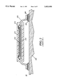
- the preferred embodiment is illustrated in FIG. 5.
- the molded body portion 710 of the TSOP package 20 has a "gull wing” or “s” shaped lead 720, that can be ultimately soldered 760 to a PWB 740.
- the package lead 720 is copper, which matches the copper pad 746 of the PWB 740. With this configuration, there is no local TCE mismatch between lead and pad at the solder interconnect interfaces.
- the ALLOY 42 die pad material 712 is not the same as that of package lead material 720.
- an electrically conducting first metal 720 for example copper
- the upper surface 721 contains a recessed area 723, into which a second metal 727 is deposited.
- the second metal 727 is a metal or alloy with a TCE less than that of the first metal 720.
- the lower surface 722 also contains a recessed feature 724, into which a second metal 728 is attached.
- the second metal 728 is a metal or alloy with TCE less than that of the first metal 720.
- the second conductive metal insert portions 727 and 728 can be any of the materials listed in TABLE I that have a TCE less than the 16.8 ppm/° C. of copper, and preferably ALLOY 42, Alloy 52, KOVAR, iron, nickel or gold.
- KOVAR® is a registered trademark of the Westinghouse Electric Corporation, and has a composition of approximately 29% nickel, 17% cobalt and the balance iron; ALLOY 42 has a composition of approximately 42% nickel and approximately 57% iron; ALLOY 52 has a composition of approximately 52% nickel and the balance iron.
- the location of the second metal 727 on the upper surface is on the convex surface, or exterior of one knee, or outer largest radius of curvature, of the formed gull wing.
- the location of the second metal 728 on the second opposing surface is on the exterior of the other knee, or outer largest radius of curvature of the formed gull wing. Since the TCE of the second metal is smaller than the TCE of the first metal 720, it will partially straighten the lead, thus lengthening the lead, as the temperature increases. Likewise, this metallic insert and difference of expansion characteristics will increase the lead bending, and thus shorten the lead length, as the temperature decreases, in order to match the expansion and contraction of the PWB 740.
- One alternate method of minimizing this thermally imposed stress is to make the portion of the lead frame that the die is mounted to (the die pad) out of a material that matches the TCE of the IC, and then make the leads out of a material that more closely approximates the TCE of the substrate.
- the die pad portion would be ALLOY 42, and the leads would be copper.
- FIG. 4 is an alternate embodiment of the invention, illustrating a portion of the molded body portion 610 of a TSOP package 20, and a "gull wing” or “s” shaped TSOP lead 620, that is soldered 660 to a PWB 640.
- the ALLOY 42 die pad material 612 is the same as that of package lead material 620.
- the multiple coplanar "gull wing" or “s” shaped leads 620 of this integrated circuit package comprise: an electrically conducting shaped member or lead 620 made of, for example ALLOY 42, having upper surface 621, and lower surface 622.
- One portion 623 of the upper surface 621 contains a metal or metal alloy 627 that is attached to the lead, and which has a TCE greater than that of the lead.
- Another portion 624 of the lead 620 contains a metal or metal alloy 628 that is attached to the lead and has a TCE greater than that of the lead.
- a third metal 626 is attached to another portion of lead 620, at the lead end so that it will become the surface that solder interconnects to the copper land 646.
- Metal 626 is copper, and matches the TCE of PWB land 646, in order to remove local stress in the solder interconnect due to dissimilar metals.
- the metal insert portions 627 and 628 can be any of the materials listed above that are greater than 4.2 ppm/° C., preferably copper, nickel, aluminum, or Alloy 52
- the location of the both the metals 627 and 628 is at the concave or inner or smallest radius of curvature of the formed gull wing.
- the thermal expansion characteristics of the metals are greater than the thermal expansion characteristics of the lead 620, and will partially straighten the lead, and thus lengthen the lead, as the temperature increases. Conversely, this metallic insert location and difference in expansion characteristics will increase the lead bending, and thus shorten the lead length, as the temperature decreases, in order to match the expansion and contraction of the PWB 640.
- the instant invention solves the problems of TCE mismatch between the TSOP and the PWB encountered in the prior art.
- the stress on the accompanying solder joint is reduced, thereby increasing the life and reliability of the assembled component, and thus, improving the electronic product.
- the exterior surfaces of all package leads may be provided to be solderable surfaces. This is consistent with the present state of the art in electronic packaging, and can be achieved by electroplating a coating of tin, silver, gold, or tin/lead alloy, or tinning in molten solder. Numerous modifications, changes, variations, substitutions and equivalents will occur to those skilled in the art without departing from the spirit and scope of the present invention as defined by the appended claims. Although only one lead shape has been shown in the drawings, other configurations may be substituted, and still fall within the scope of the invention.
Abstract
Description
              TABLE 1
______________________________________
Metal/Alloy          TCE
______________________________________
Copper               16.8   ppm/°C.
Silver               19.6   ppm/°C.
ALLOY 42             4.3    ppm/°C.
Nickel ALLOY 52      9.95   ppm/°C.
Aluminum             23.9   ppm/°C.
Gold                 14.2   ppm/°C.
Iron                 12.2   ppm/°C.
KOVAR                5.9    ppm/°C.
Nickel               13.3   ppm/°C.
______________________________________
Claims (14)
Priority Applications (1)
| Application Number | Priority Date | Filing Date | Title |
|---|---|---|---|
| US08/268,368 US5455446A (en) | 1994-06-30 | 1994-06-30 | Leaded semiconductor package having temperature controlled lead length |
Applications Claiming Priority (1)
| Application Number | Priority Date | Filing Date | Title |
|---|---|---|---|
| US08/268,368 US5455446A (en) | 1994-06-30 | 1994-06-30 | Leaded semiconductor package having temperature controlled lead length |
Publications (1)
| Publication Number | Publication Date |
|---|---|
| US5455446A true US5455446A (en) | 1995-10-03 |
Family
ID=23022684
Family Applications (1)
| Application Number | Title | Priority Date | Filing Date |
|---|---|---|---|
| US08/268,368 Expired - Fee Related US5455446A (en) | 1994-06-30 | 1994-06-30 | Leaded semiconductor package having temperature controlled lead length |
Country Status (1)
| Country | Link |
|---|---|
| US (1) | US5455446A (en) |
Cited By (14)
| Publication number | Priority date | Publication date | Assignee | Title |
|---|---|---|---|---|
| US5654585A (en) * | 1994-09-30 | 1997-08-05 | Nec Corporation | Semiconductor device with at least one lead having a plurality of bent portions |
| US5786548A (en) * | 1996-08-15 | 1998-07-28 | Hughes Electronics Corporation | Hermetic package for an electrical device |
| US5844305A (en) * | 1994-01-13 | 1998-12-01 | Samsung Electronics Co., Ltd. | Lead frame for semiconductor devices |
| US6000126A (en) * | 1996-03-29 | 1999-12-14 | General Dynamics Information Systems, Inc. | Method and apparatus for connecting area grid arrays to printed wire board |
| US6150712A (en) * | 1998-01-09 | 2000-11-21 | Sony Corporation | Lead frame for semiconductor device, and semiconductor device |
| US6441477B2 (en) * | 2000-07-24 | 2002-08-27 | Mitsubishi Denki Kabushiki Kaisha | Substrate mounting an integrated circuit package with a deformed lead |
| US20020121680A1 (en) * | 2001-03-05 | 2002-09-05 | Samsung Electronics Co., Ltd. | Ultra-thin semiconductor package device and method for manufacturing the same |
| US20030038361A1 (en) * | 2001-08-23 | 2003-02-27 | Akio Nakamura | Semiconductor apparatus and method for fabricating the same |
| US20090057850A1 (en) * | 2007-09-05 | 2009-03-05 | Wai Hoong Moy | Surface Mountable Semiconductor Package with Solder Bonding Features |
| US20110037179A1 (en) * | 2008-02-01 | 2011-02-17 | Imec | Semiconductor package |
| US20110075386A1 (en) * | 2009-09-30 | 2011-03-31 | Fujitsu Limited | Electronic component, board unit, and information-processing device |
| US20140268603A1 (en) * | 2013-03-12 | 2014-09-18 | International Business Machines Corporation | Area array device connection structures with complimentary warp characteristics |
| US20170245404A1 (en) * | 2016-02-19 | 2017-08-24 | Alpha Assembly Solutions Inc. | Rf shield with selectively integrated solder |
| US20200235042A1 (en) * | 2019-01-23 | 2020-07-23 | Texas Instruments Incorporated | Electronic device with lead pitch gap |
Citations (7)
| Publication number | Priority date | Publication date | Assignee | Title |
|---|---|---|---|---|
| JPS61241956A (en) * | 1985-04-19 | 1986-10-28 | Hitachi Ltd | Semiconductor device |
| US4673967A (en) * | 1985-01-29 | 1987-06-16 | Texas Instruments Incorporated | Surface mounted system for leaded semiconductor devices |
| JPH01289151A (en) * | 1988-05-16 | 1989-11-21 | Toshiba Corp | Integrated circuit device |
| JPH0373562A (en) * | 1989-08-14 | 1991-03-28 | Hitachi Ltd | Electronic parts and lead frame therefor |
| US5041901A (en) * | 1989-05-10 | 1991-08-20 | Hitachi, Ltd. | Lead frame and semiconductor device using the same |
| US5329158A (en) * | 1990-03-23 | 1994-07-12 | Motorola Inc. | Surface mountable semiconductor device having self loaded solder joints |
| US5360991A (en) * | 1993-07-29 | 1994-11-01 | At&T Bell Laboratories | Integrated circuit devices with solderable lead frame |
-
1994
- 1994-06-30 US US08/268,368 patent/US5455446A/en not_active Expired - Fee Related
Patent Citations (7)
| Publication number | Priority date | Publication date | Assignee | Title |
|---|---|---|---|---|
| US4673967A (en) * | 1985-01-29 | 1987-06-16 | Texas Instruments Incorporated | Surface mounted system for leaded semiconductor devices |
| JPS61241956A (en) * | 1985-04-19 | 1986-10-28 | Hitachi Ltd | Semiconductor device |
| JPH01289151A (en) * | 1988-05-16 | 1989-11-21 | Toshiba Corp | Integrated circuit device |
| US5041901A (en) * | 1989-05-10 | 1991-08-20 | Hitachi, Ltd. | Lead frame and semiconductor device using the same |
| JPH0373562A (en) * | 1989-08-14 | 1991-03-28 | Hitachi Ltd | Electronic parts and lead frame therefor |
| US5329158A (en) * | 1990-03-23 | 1994-07-12 | Motorola Inc. | Surface mountable semiconductor device having self loaded solder joints |
| US5360991A (en) * | 1993-07-29 | 1994-11-01 | At&T Bell Laboratories | Integrated circuit devices with solderable lead frame |
Non-Patent Citations (2)
| Title |
|---|
| Semiconductor International, May 1994, "Ultrathin Packages: Are They Ahead of Their Time?", pp. 48-52. |
| Semiconductor International, May 1994, Ultrathin Packages: Are They Ahead of Their Time , pp. 48 52. * |
Cited By (22)
| Publication number | Priority date | Publication date | Assignee | Title |
|---|---|---|---|---|
| US5844305A (en) * | 1994-01-13 | 1998-12-01 | Samsung Electronics Co., Ltd. | Lead frame for semiconductor devices |
| US5654585A (en) * | 1994-09-30 | 1997-08-05 | Nec Corporation | Semiconductor device with at least one lead having a plurality of bent portions |
| US6000126A (en) * | 1996-03-29 | 1999-12-14 | General Dynamics Information Systems, Inc. | Method and apparatus for connecting area grid arrays to printed wire board |
| US5786548A (en) * | 1996-08-15 | 1998-07-28 | Hughes Electronics Corporation | Hermetic package for an electrical device |
| US6150712A (en) * | 1998-01-09 | 2000-11-21 | Sony Corporation | Lead frame for semiconductor device, and semiconductor device |
| US6441477B2 (en) * | 2000-07-24 | 2002-08-27 | Mitsubishi Denki Kabushiki Kaisha | Substrate mounting an integrated circuit package with a deformed lead |
| US20020121680A1 (en) * | 2001-03-05 | 2002-09-05 | Samsung Electronics Co., Ltd. | Ultra-thin semiconductor package device and method for manufacturing the same |
| US7012325B2 (en) * | 2001-03-05 | 2006-03-14 | Samsung Electronics Co., Ltd. | Ultra-thin semiconductor package device and method for manufacturing the same |
| US20030038361A1 (en) * | 2001-08-23 | 2003-02-27 | Akio Nakamura | Semiconductor apparatus and method for fabricating the same |
| US7239008B2 (en) * | 2001-08-23 | 2007-07-03 | Oki Electric Industry Co., Ltd. | Semiconductor apparatus and method for fabricating the same |
| US20090057850A1 (en) * | 2007-09-05 | 2009-03-05 | Wai Hoong Moy | Surface Mountable Semiconductor Package with Solder Bonding Features |
| US7737546B2 (en) * | 2007-09-05 | 2010-06-15 | Avago Technologies Ecbu Ip (Singapore) Pte. Ltd. | Surface mountable semiconductor package with solder bonding features |
| US20110037179A1 (en) * | 2008-02-01 | 2011-02-17 | Imec | Semiconductor package |
| US8450825B2 (en) * | 2008-02-01 | 2013-05-28 | Imec | Semiconductor package |
| US20110075386A1 (en) * | 2009-09-30 | 2011-03-31 | Fujitsu Limited | Electronic component, board unit, and information-processing device |
| US8547706B2 (en) * | 2009-09-30 | 2013-10-01 | Fujitsu Limited | Electronic component, board unit, and information-processing device |
| US20140268603A1 (en) * | 2013-03-12 | 2014-09-18 | International Business Machines Corporation | Area array device connection structures with complimentary warp characteristics |
| US9247636B2 (en) * | 2013-03-12 | 2016-01-26 | International Business Machines Corporation | Area array device connection structures with complimentary warp characteristics |
| US9609744B2 (en) | 2013-03-12 | 2017-03-28 | International Business Machines Corporation | Area array device connection structures with complimentary warp characteristics |
| US20170245404A1 (en) * | 2016-02-19 | 2017-08-24 | Alpha Assembly Solutions Inc. | Rf shield with selectively integrated solder |
| US20200235042A1 (en) * | 2019-01-23 | 2020-07-23 | Texas Instruments Incorporated | Electronic device with lead pitch gap |
| US11569152B2 (en) * | 2019-01-23 | 2023-01-31 | Texas Instruments Incorporated | Electronic device with lead pitch gap |
Similar Documents
| Publication | Publication Date | Title |
|---|---|---|
| US5367124A (en) | Compliant lead for surface mounting a chip package to a substrate | |
| US5455446A (en) | Leaded semiconductor package having temperature controlled lead length | |
| US6538214B2 (en) | Method for manufacturing raised electrical contact pattern of controlled geometry | |
| US5757071A (en) | C4 substrate contact pad which has a layer of Ni-B plating | |
| US7005731B2 (en) | Plastic lead frames for semiconductor devices and packages including same | |
| US5774341A (en) | Solderless electrical interconnection including metallized hook and loop fasteners | |
| US6011313A (en) | Flip chip interconnections on electronic modules | |
| CN1312748C (en) | Method for mfg. semiconductor integrated circuit device | |
| US7268415B2 (en) | Semiconductor device having post-mold nickel/palladium/gold plated leads | |
| US20050151238A1 (en) | Three-level leadframe for no-lead packages | |
| JPH01313969A (en) | Semiconductor device | |
| KR20070027625A (en) | Flexible leadframe structure and method for forming integrated circuit packages | |
| US8399996B2 (en) | Chip carrier | |
| US6962836B2 (en) | Method of manufacturing a semiconductor device having leads stabilized during die mounting | |
| US6518647B1 (en) | Plated aluminum leadframes for semiconductor devices, including two nickel layers, and method of fabrication | |
| US6747343B2 (en) | Aluminum leadframes with two nickel layers | |
| JP3243684B2 (en) | Device mounting structure | |
| JPH05175406A (en) | Semiconductor integrated circuit device | |
| US11189550B2 (en) | Low-cost semiconductor package using conductive metal structure | |
| JPS60200545A (en) | Mounting substrate | |
| KR19990025537A (en) | Leadframes for Integrated Circuits | |
| JP2005150655A (en) | Lead frame, semiconductor device using the same, and method for packaging semiconductor device | |
| JPH0412597A (en) | Film carrier | |
| JPH05226543A (en) | Protective coating for lead frame use | |
| KR19990059687A (en) | Copper Plated Leadframe |
Legal Events
| Date | Code | Title | Description |
|---|---|---|---|
| AS | Assignment |
Owner name: MOTOROLA, INC., ILLINOIS Free format text: ASSIGNMENT OF ASSIGNORS INTEREST;ASSIGNORS:SUPPELSA, ANTHONY B.;DARVEAUX, ROBERT F.;WEISS, MICHAEL L.;REEL/FRAME:007079/0568;SIGNING DATES FROM 19940623 TO 19940627 |
|
| FPAY | Fee payment |
Year of fee payment: 4 |
|
| FPAY | Fee payment |
Year of fee payment: 8 |
|
| AS | Assignment |
Owner name: FREESCALE SEMICONDUCTOR, INC., TEXAS Free format text: ASSIGNMENT OF ASSIGNORS INTEREST;ASSIGNOR:MOTOROLA, INC.;REEL/FRAME:015698/0657 Effective date: 20040404 Owner name: FREESCALE SEMICONDUCTOR, INC.,TEXAS Free format text: ASSIGNMENT OF ASSIGNORS INTEREST;ASSIGNOR:MOTOROLA, INC.;REEL/FRAME:015698/0657 Effective date: 20040404 |
|
| AS | Assignment |
Owner name: CITIBANK, N.A. AS COLLATERAL AGENT, NEW YORK Free format text: SECURITY AGREEMENT;ASSIGNORS:FREESCALE SEMICONDUCTOR, INC.;FREESCALE ACQUISITION CORPORATION;FREESCALE ACQUISITION HOLDINGS CORP.;AND OTHERS;REEL/FRAME:018855/0129 Effective date: 20061201 Owner name: CITIBANK, N.A. AS COLLATERAL AGENT,NEW YORK Free format text: SECURITY AGREEMENT;ASSIGNORS:FREESCALE SEMICONDUCTOR, INC.;FREESCALE ACQUISITION CORPORATION;FREESCALE ACQUISITION HOLDINGS CORP.;AND OTHERS;REEL/FRAME:018855/0129 Effective date: 20061201 |
|
| REMI | Maintenance fee reminder mailed | ||
| LAPS | Lapse for failure to pay maintenance fees | ||
| STCH | Information on status: patent discontinuation |
Free format text: PATENT EXPIRED DUE TO NONPAYMENT OF MAINTENANCE FEES UNDER 37 CFR 1.362 |
|
| FP | Lapsed due to failure to pay maintenance fee |
Effective date: 20071003 |
|
| AS | Assignment |
Owner name: FREESCALE SEMICONDUCTOR, INC., TEXAS Free format text: PATENT RELEASE;ASSIGNOR:CITIBANK, N.A., AS COLLATERAL AGENT;REEL/FRAME:037354/0225 Effective date: 20151207 |